US8837200B2 - Nonvolatile semiconductor memory device and read method for the same - Google Patents
Nonvolatile semiconductor memory device and read method for the same Download PDFInfo
- Publication number
- US8837200B2 US8837200B2 US13/700,346 US201213700346A US8837200B2 US 8837200 B2 US8837200 B2 US 8837200B2 US 201213700346 A US201213700346 A US 201213700346A US 8837200 B2 US8837200 B2 US 8837200B2
- Authority
- US
- United States
- Prior art keywords
- offset
- electrical signal
- value
- bit line
- cell
- Prior art date
- Legal status (The legal status is an assumption and is not a legal conclusion. Google has not performed a legal analysis and makes no representation as to the accuracy of the status listed.)
- Active, expires
Links
Images


Classifications
-
- G—PHYSICS
- G11—INFORMATION STORAGE
- G11C—STATIC STORES
- G11C13/00—Digital stores characterised by the use of storage elements not covered by groups G11C11/00, G11C23/00, or G11C25/00
- G11C13/0002—Digital stores characterised by the use of storage elements not covered by groups G11C11/00, G11C23/00, or G11C25/00 using resistive RAM [RRAM] elements
- G11C13/0021—Auxiliary circuits
- G11C13/004—Reading or sensing circuits or methods
-
- G—PHYSICS
- G11—INFORMATION STORAGE
- G11C—STATIC STORES
- G11C13/00—Digital stores characterised by the use of storage elements not covered by groups G11C11/00, G11C23/00, or G11C25/00
- G11C13/0002—Digital stores characterised by the use of storage elements not covered by groups G11C11/00, G11C23/00, or G11C25/00 using resistive RAM [RRAM] elements
- G11C13/0004—Digital stores characterised by the use of storage elements not covered by groups G11C11/00, G11C23/00, or G11C25/00 using resistive RAM [RRAM] elements comprising amorphous/crystalline phase transition cells
-
- G—PHYSICS
- G11—INFORMATION STORAGE
- G11C—STATIC STORES
- G11C13/00—Digital stores characterised by the use of storage elements not covered by groups G11C11/00, G11C23/00, or G11C25/00
- G11C13/0002—Digital stores characterised by the use of storage elements not covered by groups G11C11/00, G11C23/00, or G11C25/00 using resistive RAM [RRAM] elements
- G11C13/0007—Digital stores characterised by the use of storage elements not covered by groups G11C11/00, G11C23/00, or G11C25/00 using resistive RAM [RRAM] elements comprising metal oxide memory material, e.g. perovskites
-
- G—PHYSICS
- G11—INFORMATION STORAGE
- G11C—STATIC STORES
- G11C13/00—Digital stores characterised by the use of storage elements not covered by groups G11C11/00, G11C23/00, or G11C25/00
- G11C13/0002—Digital stores characterised by the use of storage elements not covered by groups G11C11/00, G11C23/00, or G11C25/00 using resistive RAM [RRAM] elements
- G11C13/0009—RRAM elements whose operation depends upon chemical change
- G11C13/0011—RRAM elements whose operation depends upon chemical change comprising conductive bridging RAM [CBRAM] or programming metallization cells [PMCs]
-
- G—PHYSICS
- G11—INFORMATION STORAGE
- G11C—STATIC STORES
- G11C13/00—Digital stores characterised by the use of storage elements not covered by groups G11C11/00, G11C23/00, or G11C25/00
- G11C13/0002—Digital stores characterised by the use of storage elements not covered by groups G11C11/00, G11C23/00, or G11C25/00 using resistive RAM [RRAM] elements
- G11C13/0021—Auxiliary circuits
- G11C13/003—Cell access
-
- G—PHYSICS
- G11—INFORMATION STORAGE
- G11C—STATIC STORES
- G11C11/00—Digital stores characterised by the use of particular electric or magnetic storage elements; Storage elements therefor
- G11C11/02—Digital stores characterised by the use of particular electric or magnetic storage elements; Storage elements therefor using magnetic elements
- G11C11/16—Digital stores characterised by the use of particular electric or magnetic storage elements; Storage elements therefor using magnetic elements using elements in which the storage effect is based on magnetic spin effect
- G11C11/165—Auxiliary circuits
- G11C11/1673—Reading or sensing circuits or methods
-
- G—PHYSICS
- G11—INFORMATION STORAGE
- G11C—STATIC STORES
- G11C13/00—Digital stores characterised by the use of storage elements not covered by groups G11C11/00, G11C23/00, or G11C25/00
- G11C13/0002—Digital stores characterised by the use of storage elements not covered by groups G11C11/00, G11C23/00, or G11C25/00 using resistive RAM [RRAM] elements
- G11C13/0021—Auxiliary circuits
- G11C13/004—Reading or sensing circuits or methods
- G11C2013/0054—Read is performed on a reference element, e.g. cell, and the reference sensed value is used to compare the sensed value of the selected cell
-
- G—PHYSICS
- G11—INFORMATION STORAGE
- G11C—STATIC STORES
- G11C2213/00—Indexing scheme relating to G11C13/00 for features not covered by this group
- G11C2213/70—Resistive array aspects
- G11C2213/77—Array wherein the memory element being directly connected to the bit lines and word lines without any access device being used
Definitions
- the present invention relates to cross-point nonvolatile semiconductor memory devices including variable resistance memory elements, and particularly relates to a cell array structure which improves the judging function of read signals and to a read method for use in the cell array structure.
- variable resistance memory element indicates an element which has a resistance value changing according to electrical signals, has properties of keeping the resistance value even when the electrical signals are no longer supplied (that is, keeping the resistance value in a nonvolatile manner), and is capable of storing data using a change in this resistance value.
- variable resistance memory element examples include a magnetic random access memory (MRAM), a phase change random access memory (PRAM), a resistance random access memory (ReRAM; a variable resistance element), a spin transfer torque random access memory (SPRAM), and a conductive bridge random access memory (CBRAM).
- MRAM magnetic random access memory
- PRAM phase change random access memory
- ReRAM resistance random access memory
- SPRAM spin transfer torque random access memory
- CBRAM conductive bridge random access memory
- a cross-point structure As an example of the structures of the nonvolatile memory devices which include these variable resistance memory elements, a cross-point structure is known.
- memory cells are arranged each of which has two terminals and is located at a cross-point between a bit line and a word line that are perpendicular to each other; the memory cell is located between the bit line and the word line.
- the memory cell is configured with a memory element that includes a variable resistance memory element as its single element or includes a series-connected combination of a variable resistance memory element with a two-terminal switching element, such as a diode, such that the memory element has one electrode connected to the word line and the other electrode connected to the bit line.
- the cross-point structure is characterized by being suitable for large-scale integration as compared to what is called the 1T1R structure in which each variable resistance memory element is connected to a bit line via an access transistor having three terminals.
- the memory cells are arranged in an array (which is hereinafter referred to as a cross-point cell array).
- a cross-point cell array to detect (read) a resistance value of a memory element included in a target memory cell, a voltage is applied to a corresponding set of the bit line and the word line, which causes a current to flow not only in the target memory cell, but also in the other memory cells which are connected in parallel by upper and lower bit and word lines.
- the current flowing across the other memory cells is called a sneak current herein.
- the current detected upon reading always includes offset current (that is a sneak current) of which a value is always not constant. This sneak current impairs accurate detecting of the resistance value of the memory element included in the target memory cell to be read.
- this sneak current can be reduced to some extent.
- the sneak current increases according to the size of the cross-point cell array, which means that the sneak current is an impediment to the enlargement of the cross-point cell array.
- Patent Literature (PTL) 1 discloses a memory device configured to reduce sneak current-induced sensitivity deterioration in detecting a resistance value of the memory element included in the memory cell.
- a cross-point cell array 601 includes memory cells 602 and dummy cells 608 as shown in FIG. 18 .
- the memory cells 602 and the dummy cells 608 are not different in structure, and the memory cells connected to a bit line defined as a dummy bit line 609 are used as the dummy cells.
- the memory element is MRAM.
- a subtraction circuit 617 generates a current difference signal corresponding to a difference (Is ⁇ Ic) between a detecting electric current Is which flows through a selected bit line by application of a voltage between a selected word line and the selected bit line and an offset component electric current Ic which flows through the dummy bit line by application of a voltage between the selected word line and the dummy bit line.
- a read circuit 16 judges, based on this current difference signal, memory data stored in a selected cell 602 a.
- the offset component electric current Ic is a current having a value close to a value of the offset component included in the detecting electric current Is.
- the difference (Is ⁇ Ic) between the detecting electric current Is and the offset component electric current Ic has a high signal-to-noise ratio, with the result that the memory data stored in the selected cell 602 a can be judged with high reliability when judged based on the current difference signal corresponding to the difference (Is ⁇ Ic).
- MRAM is used as the memory element.
- the change amount of the resistance value is smaller than that in other variable resistance memory elements
- the ratio of a resistance value (HR) in a high resistance state to a resistance value (LR) in a low resistance state is approximately 1.2 to 1.4
- the current component which is included in the current flowing across the selected cell and flows as attributed to a resistance component not dependent on the stored data is greater than the current which corresponds to the stored data.
- the memory cell used in the above-described memory device is composed of the MRAM only and includes no switching elements.
- the literature discloses that the current corresponding to the data stored in the selected cell 602 a is about 1 ⁇ A while the offset component electric current Ic is about 30 ⁇ A.
- the offset component electric current included in the detecting electric current Is and the offset component electric current Ic which flows through the dummy bit line can be regarded substantially equal only when the above-described memory device satisfies the condition disclosed (that is, a condition that the electric current which is included in the current flowing across the selected cell and flows as attributed to the resistance component not dependent on the stored data has a greater value than the value of the current corresponding to the stored data and the offset component electric current has a significantly greater value than the value of the current corresponding to the data stored in the selected cell).
- the offset component electric current is desirably as small as possible from the perspective of improvement in accuracy for reading, a reduction in power consumption, a reduction in line deterioration due to electromigration (improvement in reliability), a reduction in positional dependency of the memory cell current within the array along with the voltage drop caused by line resistance, enlargement of the cross-point cell array, and so on.
- variable resistance memory device such as PRAM, ReRAM, and SPRAM
- the ratio of resistance change between the LR state and the HR state is high (around one decade or more), and the current component (the sneak current component) which is included in the current flowing across the selected cell and flows as attributed to the resistance component not dependent on the stored data has a smaller value than the value of the current corresponding to the stored data.
- the present invention has an object to provide a cross-point nonvolatile semiconductor memory device which includes a variable resistance memory element and is capable of reducing sneak current-induced sensitivity deterioration in detecting a resistance value of a memory element included in a memory cell, as well as to provide a read method for the cross-point nonvolatile semiconductor memory device.
- the nonvolatile semiconductor memory device comprises: word lines formed in parallel in a first plane; bit lines formed in parallel in a second plane and three-dimensionally crossing the word lines, the second plane being parallel to the first plane; and a cross-point cell array including cells each provided at a corresponding one of three-dimensional cross-points of the word lines and the bit lines, wherein the cells include: a memory cell including a memory element that operates as a memory by reversibly changing in resistance value between at least two states based on an electrical signal applied between a corresponding one of the word lines and a corresponding one of the bit lines; and an offset detection cell having a resistance value that is, irrespective of an electrical signal applied between a corresponding one of the word lines and a corresponding one of the bit lines, higher than the resistance value of the memory element in a high resistance state which is a state of the memory element when operating as the memory.
- the present invention can be implemented as a read method for the memory cell in the nonvolatile semiconductor memory device.
- the cross-point nonvolatile semiconductor memory device including the variable resistance memory element according to an aspect of the present invention is capable of reducing the problem of sneak current-induced sensitivity deterioration in detecting a resistance value of the memory element at the time of reading, which produces an effect of improving accuracy for reading.
- FIG. 1 schematically shows a structure of a nonvolatile semiconductor memory device according to Embodiment 1 of the present invention.
- FIG. 2 (a) in FIG. 2 is a plan view showing details of structures of a cross-point cell array, word lines, and bit lines, of the nonvolatile semiconductor memory device according to Embodiment 1 of the present invention, and (b) in FIG. 2 is a cross-sectional view showing a structure of a cross-section taken along X-X′ of (a) in FIG. 2 .
- FIG. 3 is a cross-sectional view for explaining other configuring methods for an offset detection cell in an implementation of the present invention.
- FIG. 4 is a cross-sectional view of a memory cell in an implementation of the present invention which is composed of ReRAM and an MSM diode.
- FIG. 5 is a view for explaining a read method for the nonvolatile semiconductor memory device according to Embodiment 1 of the present invention.
- FIG. 6 is a view for explaining the read method (sequel) for the nonvolatile semiconductor memory device according to Embodiment 1 of the present invention.
- FIG. 7 is a read flowchart for the nonvolatile semiconductor memory device according to Embodiment 1 of the present invention.
- FIG. 8 schematically shows a structure of a nonvolatile semiconductor memory device according to Embodiment 2 of the present invention.
- FIG. 9 schematically shows a structure of a nonvolatile semiconductor memory device according to Variation of Embodiment 2 of the present invention.
- FIG. 10 is a view for explaining a read method for the nonvolatile semiconductor memory device according to Variation of Embodiment 2 of the present invention.
- FIG. 11 is a view for explaining the read method (sequel) for the nonvolatile semiconductor memory device according to Variation of Embodiment 2 of the present invention.
- FIG. 12 is a view for explaining the read method (sequel) for the nonvolatile semiconductor memory device according to Variation of Embodiment 2 of the present invention.
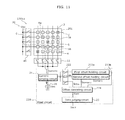
- FIG. 13 is a read flowchart for the nonvolatile semiconductor memory device according to Variation of Embodiment 2 of the present invention.
- FIG. 14 schematically shows a structure of a nonvolatile semiconductor memory device according to Embodiment 3 of the present invention.
- FIG. 15 is a view for explaining a read method for the nonvolatile semiconductor memory device according to Embodiment 3 of the present invention.
- FIG. 16 is a view for explaining the read method (sequel) for the nonvolatile semiconductor memory device according to Embodiment 3 of the present invention.
- FIG. 17 is a read flowchart for the nonvolatile semiconductor memory device according to Embodiment 3 of the present invention.
- FIG. 18 shows a structure of a conventional nonvolatile semiconductor memory device.
- a nonvolatile semiconductor memory device in an implementation of the present invention comprises: word lines formed in parallel in a first plane; bit lines formed in parallel in a second plane and three-dimensionally crossing the word lines, the second plane being parallel to the first plane; and a cross-point cell array including cells each provided at a corresponding one of three-dimensional cross-points of the word lines and the bit lines, wherein the cells include: a memory cell including a memory element that operates as a memory by reversibly changing in resistance value between at least two states based on an electrical signal applied between a corresponding one of the word lines and a corresponding one of the bit lines; and an offset detection cell having a resistance value that is, irrespective of an electrical signal applied between a corresponding one of the word lines and a corresponding one of the bit lines, higher than the resistance value of the memory element in a high resistance state which is a state of the memory element when operating as the memory.
- the offset detection cell which has a resistance value that is, irrespective of an electrical signal applied between a corresponding one of the word lines and a corresponding one of the bit lines, higher than the resistance value of the memory element in a high resistance state which is a state of the memory element when operating as a memory, with the result that subtracting the current detected when the offset detection cell is selected from the current detected when the memory element is selected leads to accurate detecting of current with the sneak current removed and thereby improves the accuracy for reading in the nonvolatile semiconductor memory device.
- the nonvolatile semiconductor memory device in an implementation of the present invention comprises: word lines formed in parallel in a first plane; bit lines formed in parallel in a second plane parallel to the first plane, and three-dimensionally crossing the word lines; a cross-point cell array including cells each provided at a corresponding one of three-dimensional cross-points of the word lines and the bit lines; a word line selector that selects one of the word lines as a selected word line; a bit line selector that selects one of the bit lines as a selected bit line; and a read circuit.
- the cells include: a memory cell including a memory element that operates as a memory by reversibly changing in resistance value between at least two states based on an electrical signal applied between a corresponding one of the word lines and a corresponding one of the bit lines; and an offset detection cell having a resistance value that is, irrespective of an electrical signal applied between a corresponding one of the word lines and a corresponding one of the bit lines, higher than the resistance value of the memory element in a state in which the memory element has the highest possible resistance when operating as the memory.
- the read circuit judges memory data stored in a read-target memory cell, based on a judging signal S NET which corresponds to a value obtained by subtracting a value of an offset electrical signal S OFFSET from a value of a memory cell electrical signal S CELL .
- the read-target memory cell is selected by the word line selector and the bit line selector from the cross-point cell array.
- the offset electrical signal S OFFSET is an electrical signal that corresponds to a value of a current flowing through a second selected bit line when a read voltage is applied between a second selected word line and the second selected bit line.
- the memory cell electrical signal S CELL is an electrical signal that corresponds to a value of a current flowing through a first selected bit line when the read voltage is applied between a first selected word line and the first selected bit line.
- the second selected word and bit lines correspond to the offset detection cell.
- the first selected word and bit lines correspond to the read-target memory cell.
- the judging signal S NET is obtained by removing, from the memory cell electrical signal S CELL , a component of the offset electrical signal S OFFSET corresponding to the offset component which changes dynamically, with the result that a significant improvement can be seen in the signal-to-noise ratio, and the accuracy for reading in the nonvolatile semiconductor memory device is higher, as compared to the case where the memory cell electrical signal S CELL is used directly as a judging signal.
- the above nonvolatile semiconductor memory device includes, as a reading process for the memory cell: a first process of determining whether data stored in the memory cell included in a cross-point cell array has been changed since detection of a value of an offset electrical signal that corresponds to a value of a current flowing through a second selected bit line when a read voltage is applied between a second selected word line and the second selected bit line; a second process of, when it is determined that the data has been changed, (i) selecting the second selected word line and the second selected bit line, (ii) detecting a value of an offset electrical signal that corresponds to a value of a current flowing through the second selected bit line, and (iii) storing the offset electrical signal into an offset holding circuit; a third process of (i) selecting the first selected word line and the first selected bit line, and (ii) detecting a value of a memory cell electrical signal that corresponds to a value of a current flowing through the first selected bit line, after completion of the first process when it is determined that the data has
- nonvolatile semiconductor memory device in another embodiment of the present invention may be configured such that offset detection cells are arranged in a one-to-one correspondence with the word lines and in a one-to-one correspondence with the bit lines.
- the read-target cell and the offset detection cell share one of the word line and the bit line, which means that the current I OFFSET detected by the offset detection cell has a value close to the value of the sneak current component I SNEAK included in the current I CELL detected when the read-target cell is selected, with the result that an improvement can be seen in the signal-to-noise ratio (Embodiment 2).
- the read circuit may have a function of judging memory data stored in a read-target memory cell, based on a judging signal which corresponds to a value obtained by subtracting, from a value of a memory cell electrical signal S CELL , a value of an offset electrical signal determined from a value of a first offset electrical signal S OFFSET1 and a value of a second offset electrical signal S OFFSET2 .
- the first offset electrical signal S OFFSET1 is an electrical signal corresponding to a value of a current flowing through a second selected bit line when a read voltage is applied between a first selected word line and the second selected bit line.
- the second offset electrical signal S OFFSET2 is an electrical signal corresponding to a value of a current flowing through the first selected bit line when the read voltage is applied between a second selected word line and the first selected bit line.
- the second selected bit line corresponds to a first offset detection cell provided for the first selected word line
- the second selected word line corresponds to a second offset detection cell provided for the first selected bit line.
- the use of two offset detection cells that is, the offset detection cell which shares a word line with the read-target memory cell and the offset detection cell which shares a bit line with the read-target memory cell, allows further accurate detecting of the offset current component in the read-target memory cell, which produces the effect of a further improvement in the signal-to-noise ratio (Variation of Embodiment 2).
- the nonvolatile semiconductor memory device in yet another embodiment of the present invention may be configured such that the bit lines include offset detection bit lines, and the offset detection cell includes offset detection cells which are arranged in the cross-point cell array in a one-to-one correspondence with the word lines and each of which is provided for one of the offset detection bit lines.
- the word lines include offset detection word lines
- the offset detection cell includes offset detection cells which are arranged in the cross-point cell array in a one-to-one correspondence with the bit lines and each of which is provided for one of the offset detection word lines.
- the bit line selector can limit the target bit lines to only the offset detection bit line while maintaining the effect of an improvement in the signal-to-noise ratio, which produces an effect of facilitating the designing of a circuit which selects a switch in the bit line selector (Embodiment 3).
- the nonvolatile semiconductor memory device does not necessarily include the word line selector, the bit line selector, and the read circuit, as long as a cross-point cell array characterized as described above is included.
- the cross-point cell array includes: a memory cell including a memory element (such as ReRAM, MRAM, PRAM, SPRAM, or CBRAM) that operates as a memory by reversibly changing in resistance value between at least two states based on an electrical signal applied between a corresponding one of the word lines and a corresponding one of the bit lines; and an offset detection cell having a resistance value that is, irrespective of an electrical signal applied between a corresponding one of the word lines and a corresponding one of the bit lines, higher than the resistance value of the memory element in a high resistance state which is a state of the memory element.
- This is a structure that can detect the sneak current with high accuracy unlike a conventional cross-point cell array which includes a memory cell and a dummy cell that are not different in structure.
- a read method for a memory cell in a nonvolatile semiconductor memory device is a read method for the memory cell in the above nonvolatile semiconductor memory device and comprises: (i) selecting a word line and a bit line between which an offset detection cell is provided, (ii) detecting a value of an offset electrical signal that corresponds to a value of a current flowing through the selected bit line, and (iii) storing the value of the offset electrical signal into an offset holding circuit; (i) selecting a word line and a bit line between which a read-target memory cell is provided, and (ii) detecting a value of a memory cell electrical signal that corresponds to a value of a current flowing through the selected bit line; calculating a judging signal by an offset canceling circuit using the value of the memory cell electrical signal and the value of the offset electrical signal held in the offset holding circuit; and judging, based on a value of the judging signal, data stored in the read-target memory cell, by a data judging
- the use of the offset detection cell provided in the cross-point cell array allows the data stored in the read-target memory cell to be judged based on the value of the memory cell electrical signal and the value of the offset electrical signal, with the result that the accuracy for reading in the nonvolatile semiconductor memory device improves.
- a nonvolatile semiconductor memory device 1000 according to Embodiment 1 of the present invention includes, as shown in FIG. 1 : word lines 2 formed in parallel in a first plane; bit lines 3 formed in parallel in a second plane parallel to the first plane, and three-dimensionally crossing the word lines 2 ; a cross-point cell array 1 including cells (a memory cell 4 and an offset detection cell 5 ) each provided at a corresponding one of three-dimensional cross-points of the word lines 2 and the bit lines 3 ; a word line selector 10 that selects one of the word lines 2 as a selected word line; a bit line selector 11 that selects one of the bit lines 3 as a selected bit line; and a read circuit 20 .
- the cells include: the memory cell 4 including a memory element that reversibly changes in resistance value between at least two states (i.e., operating as a memory) based on an electrical signal applied between a corresponding one of the word lines 2 and a corresponding one of the bit lines 3 ; and the offset detection cell 5 which has a resistance value that is, irrespective of an electrical signal applied between the corresponding word line 2 and the corresponding bit line 3 , higher than the resistance value of the memory element in a high resistance state which is a state of the memory element when operating as the memory.
- the memory cell 4 is a memory cell included in the cross-point cell array 1 , that is, a two-terminal memory cell, and includes a variable resistance memory element as its single element or includes a series-connected combination of a variable resistance memory element with a two-terminal switching element such as a diode.
- the diode may be a unidirectional diode across which a current flows only in a single direction.
- the diode may be a bidirectional diode which has a threshold voltage in each of the positive and negative directions and across which a current can flow in the both directions by application of a voltage higher than or equal to the threshold voltage.
- the read circuit 20 has a function of judging memory data stored in a read-target memory cell, based on a judging signal S NET which corresponds to a value obtained by subtracting a value of an offset electrical signal S OFFSET from a value of a memory cell electrical signal S CELL .
- the read-target memory cell is selected by the word line selector 10 and the bit line selector 11 from the cross-point cell array 1 .
- the offset electrical signal S OFFSET is an electrical signal determined from a value of a current flowing through a second selected bit line when a read voltage is applied between a second selected word line and the second selected bit line.
- the memory cell electrical signal S CELL is an electrical signal that corresponds to a value of a current flowing through a first selected bit line when the read voltage is applied between a first selected word line and the first selected bit line.
- the second selected word and bit lines correspond to the offset detection cell 5 that is at least one in number.
- the first selected word and bit lines correspond to the read-target memory cell.
- This nonvolatile semiconductor memory device 1000 includes, as described above: the word lines 2 formed in parallel; the bit lines 3 formed in parallel in the direction in which the bit lines 3 cross the word lines 2 ; and the cross-point cell array 1 formed at the cross-points, in a planar view, of the word lines 2 and the bit lines 3 and between the word lines 2 and the bit lines 3 . Furthermore, the cross-point cell array 1 includes the plurality of memory cells 4 and one or more offset detection cells 5 .
- the offset detection cell 5 is located at the center in the cross-point cell array 1 shown in FIG. 1 , the offset detection cell 5 is not necessarily located at the center and may be located at any position within the cross-point cell array 1 . Furthermore, the number of offset detection cells 5 within the cross-point cell array 1 is not limited to one, and two or more offset detection cells 5 may be provided within the single cross-point cell array 1 .
- FIG. 2 shows, in more detail, the structures of the cross-point cell array 1 , the word lines 2 , and the bit lines 3 shown in FIG. 1 .
- (a) of FIG. 2 is a plan view
- (b) of FIG. 2 shows a structure of a cross-section taken along X-X′ of (a) in FIG. 2 .
- the memory cell 4 in this embodiment includes: a memory element 111 ; a first via 110 for electrically connecting the memory element 111 and the word line 2 ; and a second via 112 for electrically connecting the memory element 111 and the bit line 3 .
- the memory element 111 includes a variable resistance memory element or a series-connected combination of a variable resistance memory element and a switching element.
- the variable resistance memory element used herein indicates an element in which a value of resistance between two terminals changes according to electrical signals and which has properties of keeping the resistance value even when the electrical signals are no longer supplied (that is, keeping the resistance value in a nonvolatile manner), and is capable of storing data by this change in resistance value.
- Usable examples of the memory element 11 specifically include a magnetic random access memory (MRAM), a phase change random access memory (PRAM), a resistance random access memory (ReRAM), a spin transfer torque random access memory (SPRAM), and a conductive bridge random access memory (CBRAM).
- MRAM magnetic random access memory
- PRAM phase change random access memory
- ReRAM resistance random access memory
- SPRAM spin transfer torque random access memory
- CBRAM conductive bridge random access memory
- the switching element herein include elements having non-linear switching properties, such as a metal-semiconductor-metal (MSM) diode which has a three-layer structure: a semiconductor layer and metal electrode layers (i.e., a first metal electrode and a second metal electrode) between which the semiconductor layer is located, a metal-insulator-metal (MIM) diode which has a three-layer structure: an insulator layer and metal electrode layers between which the insulator layer is located, a p-n junction diode which has a two-layer structure: a p-type semiconductor and an n-type semiconductor, and a Schottky diode which has a two-layer structure: a semiconductor layer and a metal electrode layer.
- MCM metal-semiconductor-metal
- MIM metal-insulator-metal
- the offset detection cell 5 has, as an example, a structure obtained by removing the second via 112 from the memory cell 4 .
- a role of the offset detection cell 5 which will be described in detail later, is to measure an approximate value of a sneak current in the cross-point cell array 1 .
- the offset detection cell 5 has a structure in which a current flowing across the offset detection cell 5 when a potential difference for reading is given between the word line 2 and the bit line 3 which are located above and below the offset detection cell 5 has a value smaller than a value of a current flowing across the memory cell 4 when a potential difference for reading is given between the word line 2 and the bit line 3 which are located above and below the memory cell 4 while the variable resistance memory element included in the memory element 111 is in a high resistance state.
- the offset detection cell 5 is configured to have a resistance value that is, irrespective of an electrical signal applied between a corresponding one of the word lines 2 and a corresponding one of the bit lines 3 , higher than the resistance value of the memory element that is included in the memory cell 4 and is in a high resistance state which is a state of the memory element when operating as a memory.
- the offset detection cell 5 shown in (b) of FIG. 2 is configured without the second via 112 as compared to the structure of the memory cell 4 such that almost no current flows across the offset detection cell 5 when a potential difference for reading is given between the word line 2 and the bit line 3 which are located above and below the offset detection cell 5 .
- the memory element 111 and an interlayer insulating film 100 thereon are formed, there is no difference in manufacture between the memory cell 4 and the offset detection cell 5 , which makes it possible eliminate the influence of variations in size and properties of resultant memory elements due to differences in layout between the memory cell 4 to which only the memory cells 4 are adjacent and the memory cell 4 to which the offset detection cell 5 is adjacent.
- FIG. 3 shows, in (a) to (d), other examples of the structure of the offset detection cell 5 .
- an offset detection cell 51 in (a) of FIG. 3 has a structure without a via for electrically connecting the memory element 111 and the word line 2 .
- An offset detection cell 52 in (b) of FIG. 3 has a structure without the memory element 111 .
- An offset detection cell 53 in (c) of FIG. 3 has a structure without both the vias for electrically connecting the memory element 11 with the word line 2 and the bit line 3 which are located above and below the offset detection cell 53 .
- an offset detection cell 54 in (d) of FIG. 3 has a structure without the memory cell, the upper via, nor the lower via.
- the current hardly flows across the offset detection cell 5 even when a potential difference for reading is given between the word line 2 and the bit line 3 which are located above and below the offset detection cell 5 , the same or like effects as those in the offset detection cell 5 shown in (b) of FIG. 2 can be obtained.
- the structures of the offset detection cells 51 to 53 in (a), (b), and (c) of FIG. 3 produce effects of reducing the possibility that the offset detection cells 51 to 53 are each short-circuited to the word line 2 in the lower layer even when a line groove which is to be the bit line 3 is overetched upon forming the bit line 3 in a damascene pattern using copper (Cu), as compared to the structure of the offset detection cell 5 shown in (b) of FIG. 2 .
- the dishing amount of the offset detection cell 52 can be the same as that of the memory cell 4 , which produces an effect of reducing local variations in focus margin in the lithography step for the memory element 111 .
- the offset detection cell 53 will not be short-circuited even when overetching occurs at the time of via etching.
- short-circuiting of the offset detection cell 54 due to variations in the manufacturing process can be prevented at the highest rate.
- the nonvolatile semiconductor memory device 1000 in FIG. 1 further includes the word line selector 10 and the bit line selector 11 .
- the word line selector 10 is connected to the word lines 2 and selects one of the word lines 2 to connect only the selected one of the word lines (that is, a selected word line) to a power supply line 6 while leaving the other word lines in the unconnected state, for example.
- potential VDD is given from a power supply 30 .
- the bit line selector 11 is connected to the bit lines 3 and selects one of the bit lines 3 to connect only the selected one of the bit lines (that is, a selected bit line) to a current sensing circuit 21 while leaving the other bit lines in the unconnected state, for example.
- the nonvolatile semiconductor memory device 1000 in FIG. 1 further includes the read circuit 20 .
- This read circuit 20 is a circuit which reads data stored in a read-target memory cell selected by the word line selector 10 and the bit line selector 11 from the cross-point cell array 1 , and includes the current sensing circuit 21 , a sensing signal selector 22 , an offset holding circuit 23 , an offset canceling circuit 24 , and a data judging circuit 25 .
- VSS potential VSS is given from a power supply 31 .
- VDD ⁇ VSS potential difference
- a current flows through the word line 2 and the bit line 3 .
- the current flowing in the bit line selector 11 -side end of the bit line selected by the bit line selector 11 is input to the current sensing circuit 21 through the bit line selector 11 .
- the current sensing circuit 21 outputs an electrical signal that corresponds to a value of the input current, that is, an electrical signal that corresponds to a value of the current flowing through the selected bit line.
- the sensing signal selector 22 has a function of selecting one of the offset holding circuit 23 and the offset canceling circuit 24 to which the electrical signal output from the current sensing circuit 21 is to be transmitted (that is, selecting where to output the electrical signal), as necessary (that is, according to an instruction given from a control circuit (not shown) included in the read circuit 20 ).
- the offset holding circuit 23 has a function of holding a value of the electrical signal (the offset electrical signal S OFFSET ) received from the current sensing circuit 21 via the sensing signal selector 22 , and outputting an electrical signal having the held value, as necessary, even when electrical signals are no longer received.
- the offset canceling circuit 24 has a function of generating an electrical signal (a judging signal) S NET that corresponds to a difference between the two input electrical signals (that is, between the memory cell electrical signal S CELL received from the current sensing circuit 21 via the sensing signal selector 22 while the memory cell 4 is selected, and the offset electrical signal S OFFSET held in the offset holding circuit 23 ).
- the data judging circuit 25 has a function of outputting an electrical signal S OUT that corresponds to “1” or “0” as memory data stored in the read-target memory cell, based on the electrical signal (the judging signal) S NET output from the offset canceling circuit 24 .
- FIG. 4 shows, as an example, a structure of the memory cell 4 which uses a variable resistance element (ReRAM) as a variable resistance memory element of the memory element 111 and an MSM diode as a switching element.
- ReRAM variable resistance element
- a variable resistance element 570 has a layered structure which includes a second electrode 512 , a high oxygen deficiency layer 521 , a low oxygen deficiency layer 522 , and a third electrode 513 .
- a diode 571 has a layered structure which includes a first electrode 511 , a semiconductor layer 530 , and the second electrode 512 .
- the second electrode 512 is shared by the variable resistance element 570 and the diode 571 in the memory element 572 shown in FIG. 4 , the second electrode 512 may have a two or more-layer structure of different materials when the variable resistance element 570 and the diode 571 need to have different electrode materials.
- tantalum nitride (TaN), titanium nitride (TiN), tungsten (W), or the like can be used, among which a 50 nm-thick TaN layer is used herein.
- the material of the third electrode 513 any one of platinum (Pt), iridium (Ir), and palladium (Pd), or an alloy thereof can be used, among which a 50-nm thick Ir layer is used herein.
- the material of the third electrode 513 is desirably a material which has a standard electrode potential higher than the standard electrode potential of a metal included in the variable resistance layer.
- the high oxygen deficiency layer 521 and the low oxygen deficiency layer 522 form the variable resistance layer of the variable resistance element 570 .
- a change in the resistance of this variable resistance layer causes a change in the resistance of the variable resistance element 570 .
- the oxygen deficiency of the low oxygen deficiency layer 522 is lower than the oxygen deficiency of the high oxygen deficiency layer 521 .
- the oxygen deficiency refers to a ratio of deficient oxygen in a transition metal relative to the amount of oxygen included in the oxide having its stoichiometric composition.
- the transition metal is tantalum (Ta)
- the stoichiometric composition of the oxide is Ta 2 O 5 , which can be expressed as TaO 2.5 .
- the oxygen deficiency of TaO 2.5 is 0%.
- the high oxygen deficiency layer 521 an oxygen-deficient film is used which is made of an oxide of which oxygen content is low in atom ratio as compared to an oxide having a stoichiometric composition; the case using a tantalum oxide is explained herein.
- the layer is formed as follows.
- the high oxygen deficiency layer 521 is made of TaO x (0 ⁇ x ⁇ 2.5) as a favorable range and is preferably 30 nm or more and 100 nm or less in thickness.
- the low oxygen deficiency layer 522 is made of TaO y (x ⁇ y) as a favorable range and is preferably 1 nm or more and 10 nm or less in thickness. It is possible to adjust the value x of TaO x in the chemical formula by adjusting the flow rate of oxygen gas relative to the flow rate of argon gas in the sputtering.
- a substrate is placed in a sputtering device which is then vacuumed to approximately 7 ⁇ 10 ⁇ 4 Pa.
- sputtering is performed with a combination of argon gas and oxygen gas at a total gas pressure of 3.3 Pa and with the substrate at set temperature of 30 degrees Celsius.
- the oxygen partial pressure changes from 1% to 7% in the ratio
- the oxygen content atomic percentage in the tantalum oxide layer i.e., the composition ratio of oxygen atoms to the total atoms (0/(Ta+0)
- the composition of the tantalum oxide layer can be measured using the Rutherford Backscattering Spectrometry.
- the oxide having its stoichiometric composition refers herein to Ta 2 O 5 , which is an insulator, in the case of the tantalum oxide.
- a metal oxide becomes electrically conductive.
- a 6 nm-thick Ta 2 O 5 film is deposited as the low oxygen deficiency layer 522
- 50 nm-thick TaO 0.66 is deposited as the high oxygen deficiency layer 521 .
- a variable resistance layer which has the same or like layered structure can be formed using, other than the oxygen-deficient tantalum oxide film, an oxide film which includes iron that is also oxygen-deficient, or other transition metal oxides which include hafnium (Hf), zirconium (Zr), titanium (Ti), niobium (Nb), or tungsten (W).
- Methods of forming these films include a sputtering method and a chemical vapor deposition (CVD) method.
- Each of the low oxygen deficiency layer 522 and the high oxygen deficiency layer 521 may be formed of, or include at least, one selected from among the above-listed plurality of oxides. Specifically, it may be that the low oxygen deficiency layer 522 includes at least one of an oxygen-deficient tantalum oxide film, an oxygen-deficient iron oxide film, an oxygen-deficient hafnium oxide film, and an oxygen-deficient zirconium oxide, and the high oxygen deficiency layer 521 includes at least one of an oxygen-deficient tantalum oxide film, an oxygen-deficient iron oxide film, an oxygen-deficient hafnium oxide film, and an oxygen-deficient zirconium oxide.
- a transition metal has a plurality of states of oxidation and is therefore allowed to provide different resistance states by oxidation-reduction reactions.
- the resistance value of the variable resistance layer can stably change at high speed when x in the composition HfO x of the high oxygen deficiency layer 521 is 0.9 or more and 1.6 or less and y in the composition HfO y of the low oxygen deficiency layer 522 is larger than x.
- the thickness of the low oxygen deficiency layer 522 is preferably 3 nm or more and 4 nm or less in thickness.
- the resistance value of the variable resistance layer can stably change at high speed when x in the composition ZrO x of the high oxygen deficiency layer 521 is 0.9 or more and 1.4 or less and y in the composition ZrO y of the low oxygen deficiency layer 522 is larger than x.
- the thickness of the low oxygen deficiency layer 522 is preferably 1 nm or more and 5 nm or less.
- variable resistance layer As above which has a layered structure: the low oxygen deficiency layer 522 that has high resistance and a small thickness; and the high oxygen deficiency layer 521 that has low resistance, the voltage applied to the variable resistance element is distributed more to the low oxygen deficiency layer 522 that has high resistance, which allows the oxidation-reduction in the low oxygen deficiency layer 522 to be more likely to occur.
- a first transition metal included in the high oxygen deficiency layer 521 and a second transition metal included in the low oxygen deficiency layer 522 may include different materials.
- the low oxygen deficiency layer 522 preferably has a lower degree of oxygen deficiency, that is, higher resistance, than the high oxygen deficiency layer 521 .
- the standard electrode potential of the second transition metal is preferably smaller than the standard electrode potential of the first transition metal.
- a resistance change phenomenon presumably occurs by an oxidation-reduction reaction in a tiny filament (a conductive path) formed in the low oxygen deficiency layer 522 having high resistance, which reaction changes the value of resistance.
- the high oxygen deficiency layer 521 includes an oxygen-deficient tantalum oxide and the low oxygen deficiency layer 522 includes a titanium oxide (TiO 2 )
- the standard electrode potential having a larger value represents a property of being more difficult to oxidize.
- Providing, as the low oxygen deficiency layer 522 , an oxide of a metal having a lower standard electrode potential than the standard electrode potential of the high oxygen deficiency layer 521 makes an oxidation-reduction reaction more likely to occur in the low oxygen deficiency layer 522 .
- the variable resistance layer having the above-described layered structure the initial resistance value of the variable resistance element right after manufacture is very high.
- SiN x nitrogen-deficient silicon nitride
- Such an SiN x film having a semiconductor property can be formed by reactive sputtering which uses an Si target in a nitrogen gas atmosphere, for example.
- the pressure of the chamber is set to 0.1 Pa to 1 Pa, and the flow rate Ar/N 2 is set to 18 sccm/2 sccm.
- W is used as a material of each of the first via 110 and the second via 112 .
- Examples of an interlayer insulating film 501 include a TEOS-SiO film, a silicon nitride (SiN) film, a low dielectric constant material, such as a silicon carbonitride (SiCN) film or a silicon oxycarbide (SiOC) film, or a fluorinated silicon oxide (SiOF) film. Furthermore, a layered structure in which these materials are stacked may be used. Herein, the TEOS-SiO film is used.
- the word lines 2 and the bit lines 3 copper (Cu) lines, aluminum-copper alloy (Al—Cu) lines, and the like which are used in typical semiconductors can be used.
- Al—Cu lines are used.
- the resistance value of the variable resistance element 570 with the above structure right after manufacture (the initial resistance value) is higher than a resistance value thereof in a high resistance (HR) state at the time of normal resistance change operation.
- HR high resistance
- variable resistance element Since the initial resistance value of the variable resistance element which is used as a memory cell for storing data is very high right after manufacture, the variable resistance element needs to be subjected to the initial breakdown to cause a resistance change; if a certain resistance variable element is not subjected to the initial breakdown intentionally, the memory cell including the resistance variable element can be used as the offset detection cell.
- the variable resistance element 570 of FIG. 4 it is possible to manufacture the memory cell 4 and the offset detection cell 5 by selecting whether to perform the initial breakdown.
- the memory cell 4 is a cell on which the initial breakdown for causing the memory element to perform the memory operation has been performed after manufacture while the offset detection cell 5 is a cell which has the same structure as the memory cell 4 and on which no initial breakdown has been performed after manufacture.
- the offset detection cell 5 is a cell which has the same structure as the memory cell 4 and on which no initial breakdown has been performed after manufacture.
- variable resistance element 570 of FIG. 4 is used are not limited to this embodiment only and are seen in the later-described Embodiments 2 and 3.
- the following cites, as an example, the operation to read data from the read-target cell (the memory cell to be read) 4 a and describes a sequence thereof.
- the word line selector 10 connects, to the power supply line 6 , only the word line connected to the offset detection cell 5 while leaving the other word lines in the unconnected state.
- the bit line selector 11 connects, to the current sensing circuit 21 , only the bit line connected to the offset detection cell 5 while leaving the other bit lines in the unconnected state.
- the current I OFFSET which flows in the bit line selector 11 -side end of the bit line selected by the bit line selector 11 (the selected bit line) is input to the current sensing circuit 21 , and the electrical signal (the offset electrical signal) S OFFSET that corresponds to a value of the current I OFFSET is output from the current sensing circuit 21 .
- this electrical signal output from the current sensing circuit 21 is an electrical signal which changes according to a value of the current input to the current sensing circuit 21 , and the electrical signal can be freely selected in conformity with a type of a circuit determined to be used as each of the offset holding circuit 23 and the offset canceling circuit 24 .
- the amplitude of current or voltage or the pulse width or pulse density of the pulsed current or voltage may be used.
- the sensing signal selector 22 outputs the electrical signal (the offset electrical signal) S OFFSET to the offset holding circuit 23 and causes the offset holding circuit 23 to hold the offset electrical signal S OFFSET .
- the current sensing circuit 21 is disconnected from the offset canceling circuit 24 by the sensing signal selector 22 as shown in FIG. 5 .
- the word line selector 10 connects, to the power supply line 6 , only the word line which includes the read-target cell 4 a while leaving the other word lines in the unconnected state.
- the bit line selector 11 connects, to the current sensing circuit 21 , only the bit line which includes the read-target cell 4 a while leaving the other bit lines in the unconnected state.
- current I CELL which flows in the bit line selector 11 -side end of the bit line selected by the bit line selector 11 is input to the current sensing circuit 21 , and an electrical signal (a memory cell electrical signal) S CELL that corresponds to a value of the current I CELL is output from the current sensing circuit 21 .
- the sensing signal selector 22 inputs the electrical signal (the memory cell electrical signal) S CELL to the offset canceling circuit 24 .
- the current sensing circuit 21 is disconnected from the offset holding circuit 23 by the sensing signal selector 22 as shown in FIG. 6 .
- the offset holding circuit 23 is caused to output the held electrical signal (the offset electrical signal) S OFFSET to the offset canceling circuit 24 .
- This electrical signal (the judging signal) S NET is input to the data judging circuit 25 .
- the data judging circuit 25 judges, based on a value of the input electrical signal (judging signal) S NET , whether the memory element included in the read-target cell 4 a is in the high resistance (HR) state or in the low resistance (LR) state (i.e., the data stored in the read-target cell 4 a ), and outputs, as an output signal of the read circuit 20 , an electrical signal S OUT that corresponds to “1” or “0” to outside.
- the current component I 0 which flows across the read-target cell 4 a changes depending on the data stored in the memory element included in the read-target cell 4 a , that is, whether the memory element is in the high resistance (HR) state or in the low resistance (LR) state, and has a larger value when the memory element is in the LR state.
- the sneak current component I SNEAK is hardly influenced by the data stored in the memory element included in the read-target cell 4 a , but changes depending on the data stored in all the memory cells 4 except the read-target cell 4 a in the cross-point cell array 1 , and the value of the sneak current component I SNEAK is the largest when the memory elements in all the memory cells 4 except the read-target cell 4 a are in the LR state while it is the smallest when the memory elements in all the memory cells 4 except the read-target cell 4 a are in the HR state. Furthermore, an increase in the size of the cross-point cell array 1 accompanies an increase in the sneak current component I SNEAK .
- the current I CELL has a low signal-to-noise ratio and is largely influenced by the sneak current component I SNEAK .
- I LR I CELL when the memory element in the read-target cell 4 a is in the LR state
- I HR I CELL when the memory element in the read-target cell 4 a is in the HR state
- the sneak current component I SNEAK not only changes depending on the size of the cross-point cell array 1 , but also dynamically changes depending on the data stored in the cross-point cell array 1 .
- the signal-to-noise ratio is determined with the sneak current component I SNEAK having the largest value.
- the size of the cross-point cell array is determined so that the maximum value of the sneak current component I SNEAK becomes smaller than or equal to I LR .
- the current (the offset current) I OFFSET that is input to the current sensing circuit 21 when the word line selector 10 and the bit line selector 11 select the word line and the bit line, respectively, which include the offset detection cell 5 is (I 1 +I SNEAK ).
- I 1 represents a current component which flows across the offset detection cell 5 and satisfies I 1 ⁇ I HR .
- I 1 ⁇ 0 is satisfied, which leads to I OFFSET ⁇ I SNEAK , meaning that the offset current I OFFSET includes the sneak current component I SNEAK only.
- This sneak current component I SNEAK detected using the offset current I OFFSET does not exactly match the sneak current component I SNEAK included in the current I CELL , but its difference decreases as the size of the cross-point cell array 1 increases.
- the offset current I OFFSET approximately equals the offset current component that is included in the read-target cell 4 a in the cross-point cell array 1 and dynamically changes.
- the offset detection cell desirably has one of the structures shown in FIGS. 2 and 3 because the effects increase as I 1 decreases.
- the judging signal S NET for judging data results from removing, from the memory cell electrical signal S CELL , a component of the offset electrical signal S OFFSET corresponding to the offset component which changes dynamically, with the result that a significant improvement can be seen in the signal-to-noise ratio, and the accuracy for reading in the nonvolatile semiconductor memory device 1000 is higher, as compared to the case where the memory cell electrical signal S CELL is used directly as a judging signal.
- FIG. 7 is a flowchart showing a flow for reading in the nonvolatile semiconductor memory device 1000 according to Embodiment 1 of the present invention.
- This offset electrical signal S OFFSET changes dynamically depending on the data stored in the cross-point cell array 1 ; conversely, unless the data stored in the cross-point cell array 1 changes, the offset electrical signal S OFFSET held in the offset holding circuit 23 can continue to be used also in reading next data. In this case, the operation to select the offset detection cell 5 and detect the offset electrical signal S OFFSET can be omitted.
- the offset detection cell 5 is selected to detect the offset electrical signal S OFFSET (F 2 ; the first half of an offset detecting process), and the detected signal is stored into the offset holding circuit 23 (F 3 ; the latter half of the offset detecting process).
- Step F 1 is completed when it is determined in Step F 1 that there is no change in the data (No in F 1 ) or after Step F 3 is completed when it is determined that there is a change in the data (Yes in F 1 )
- the read-target cell 4 a is selected to read the memory cell electrical signal S CELL (F 4 ; a memory cell detecting process)
- the offset canceling circuit 24 the difference signal (the judging signal) S NET between the read memory cell electrical signal S CELL and the offset electrical signal S OFFSET is calculated (F 5 ; an offset canceling process).
- the data judging circuit 25 the data stored in the read-target cell 4 a is judged using the difference signal (the judging signal) S NET (F 6 ; a data judging process). With that, the operation to read data is completed.
- the present invention is not limited to the case where the number of offset detection cells 5 is one.
- the cross-point cell array 1 may further be divided into some sub regions in each of which the offset detection cell 5 is provided so that the offset electrical signal S OFFSET for each sub region is detected and then used to generate a judging signal.
- FIG. 8 shows, as an example, a structure of a nonvolatile semiconductor memory device 1001 according to Embodiment 2 of the present invention.
- a difference between the nonvolatile semiconductor memory device 1001 according to this embodiment and the nonvolatile semiconductor memory device 1000 according to Embodiment 1 is that a plurality of offset detection cells 5 are provided within a cross-point cell array 201 in a manner that one offset detection cell 5 is connected to each of the word lines 2 and each of the bit lines 3 .
- the offset detection cells 5 are arranged in the cross-point cell array 201 so that they correspond one-to-one with the word lines 2 and one-to-one with the bit lines 3 .
- Each of the memory cell 4 and the offset detection cell 5 may have the same structure as that described in Embodiment 1.
- the offset current component included in the detecting current for the read-target cell can be detected as the current detected by the offset detection cell 5 connected to the bit line 3 or the word line 2 which includes the target memory cell 4 . This produces an effect of further accurate detecting of the offset current component in the read-target memory cell as compared to the case described in Embodiment 1.
- the nonvolatile semiconductor memory device 1001 according to Embodiment 2 of the present invention includes, as shown in FIG. 8 : the word lines 2 formed in parallel; the bit lines 3 formed in parallel in the direction in which the bit lines 3 cross the word lines 2 ; and the cross-point cell array 201 formed at the cross-points, in a planar view, of the word lines 2 and the bit lines 3 and between the word lines 2 and the bit lines 3 .
- the cross-point cell array 201 includes the plurality of memory cells 4 and the plurality of offset detection cells 5 .
- the offset detection cells 5 are arranged within the cross-point cell array 201 in a manner that one offset detection cell 5 is connected to each of the word lines 2 and each of the bit lines 3 .
- the offset detection cells 5 in the cross-point cell array 201 of FIG. 8 are regularly arranged on, as the cross-points of the word lines 2 and the bit lines 3 , a diagonal of the cross-point cell array 201 herein, the arrangement is not limited thereto, and as long as one offset detection cell is connected to each of the word lines 2 and each of the bit lines 3 , the arrangement of the offset detection cells is not limited to the arrangement on the diagonal of the cross-point cell array 201 .
- the word line selector 10 , the bit line selector 11 , the power supply line 6 , and the read circuit 20 included in the nonvolatile semiconductor memory device 1001 according to Embodiment 2 of the present invention may be the same as those described in Embodiment 1.
- a read method for use in the nonvolatile semiconductor memory device 1001 according to Embodiment 2 of the present invention is almost the same as the read method for use in the nonvolatile semiconductor memory device 1000 according to Embodiment 1 of the present invention, and only the differences between Embodiment 2 and Embodiment 1 in the present invention are therefore described below.
- a difference in the read method between the nonvolatile semiconductor memory devices according to Embodiment 2 and Embodiment 1 is that the word line and the bit line which the word line selector 10 and the bit line selector 11 select, respectively, upon detecting of the offset electrical signal S OFFSET are different.
- the same word line and the same bit line are always selected upon detecting of the offset electrical signal S OFFSET .
- the word line which includes the read-target cell is selected upon detecting of the offset electrical signal S OFFSET.
- the bit line which is connected to the offset detection cell connected to the selected word line is selected. It is to be noted that the same effects can be obtained even when the bit line which includes the read-target cell is selected and then the word line which is connected to the offset detection cell connected to the selected bit line is selected.
- the read circuit 20 reads data from the memory cell in one of the following methods.
- a first read method is a read method in which the memory cell 4 and the offset detection cell 5 shares the word line.
- the read circuit 20 judges the memory data stored in the read-target memory cell, based on the judging signal S NET which corresponds to a value obtained by subtracting a value of the offset electrical signal S OFFSET from a value of the memory cell electrical signal S CELL .
- the offset electrical signal S OFFSET corresponds to a value of the current flowing through the second selected bit line when the read voltage is applied between the first selected word line corresponding to the read-target memory cell and the second selected bit line corresponding to the offset detection cell provided for the first selected word line.
- a second read method is a read method in which the memory cell and the offset detection cell share the bit line.
- the read circuit 20 judges the memory data stored in the read-target memory cell, based on the judging signal S NET which corresponds to a value obtained by subtracting a value of the offset electrical signal S OFFSET from a value of the memory cell electrical signal S CELL .
- the offset electrical signal S OFFSET corresponds to a value of the current flowing through the first selected bit line when the read voltage is applied between the second selected word line corresponding to the offset detection cell provided for the first selected bit line corresponding to the read-target memory cell and the first selected bit line corresponding to the read-target memory cell.
- the sneak current component I SNEAK included in the current I CELL detected when the read-target cell is selected changes depending on the data stored in the memory cell 4 included in the cross-point cell array 201 and is influenced more by the data stored in the memory cell 4 connected to the bit line 3 and the word line 2 which are connected to the read-target cell than by the data stored in the memory cell 4 connected to neither of the bit line 3 and the word line 2 which are connected to the read-target cell.
- the offset current I OFFSET detected by the offset detection cell 5 has a value close to the sneak current component I SNEAK included in the current I CELL detected when the read-target cell is selected, with the result that, as compared to Embodiment 1, improvements can be seen in the signal-to-noise ratio and in the accuracy for reading in the nonvolatile semiconductor memory device 1001 .
- FIG. 9 shows, as an example, a structure of a nonvolatile semiconductor memory device 1001 a according to Variation of Embodiment 2 of the present invention.
- a difference between the nonvolatile semiconductor memory device 1001 a according to this variation and the nonvolatile semiconductor memory device 1001 according to Embodiment 2 is that the offset current component included in the detecting current for the read-target cell is detected with reference to two currents: a current detected by the offset detection cell connected to the word line which includes the target memory cell; and a current detected by the offset detection cell connected to the bit line which includes the target memory cell. This produces an effect of further accurate detecting of the offset current component in the read-target memory cell as compared to the case described in Embodiment 2.
- the nonvolatile semiconductor memory device 1001 a of FIG. 9 further includes a read circuit 220 .
- the read circuit 220 is a circuit which reads data stored in the read-target memory cell selected by the word line selector 10 and the bit line selector 11 from the cross-point cell array 201 , and includes the current sensing circuit 21 , a sensing signal selector 222 , a first offset holding circuit 223 a , a second offset holding circuit 223 b , an offset canceling circuit 224 , and the data judging circuit 25 .
- VSS is given from the power supply 31 .
- a potential difference VDD ⁇ VSS
- VDD ⁇ VSS a potential difference
- the current flowing in the bit line selector 11 -side end of the bit line selected by the bit line selector 11 is input to the current sensing circuit 21 through the bit line selector 11 .
- the current sensing circuit 21 outputs an electrical signal that corresponds to a value of the input current, that is, an electrical signal that corresponds to a value of the current flowing through the selected bit line.
- the sensing signal selector 222 has a function of selecting one of the first offset holding circuit 223 a , the second offset holding circuit 223 b , and the offset canceling circuit 224 to which the electrical signal output from the current sensing circuit 21 is to be transmitted (that is, selecting where to output the electrical signal), as necessary (that is, according to an instruction given from a control circuit (not shown) included in the read circuit 220 ).
- the first offset holding circuit 223 a and the second offset holding circuit 223 b have a function of holding values of the electrical signals (a first offset electrical signal S OFFSET1 and a second offset electrical signal S OFFSET2 ) received from the current sensing circuit 21 through the sensing signal selector 222 , and outputting electrical signals having the held values, as necessary, even when electrical signals are no longer received.
- the offset canceling circuit 224 has a function of generating the electrical signal (the judging signal) S NET based on the expression below by referring to the three input electrical signals: the first offset electrical signal S OFFSET1 held in the first offset holding circuit 223 a ; the second offset electrical signal S OFFSET2 held in the second offset holding circuit 223 b ; and the memory cell electrical signal S CELL received from the current sensing circuit 21 via the sensing signal selector 222 while the memory cell 4 is selected.
- the judging signal S NET determined by S NET S CELL ⁇ ( S OFFSET1 +S OFFSET2 )/2 is desirable because this leads to an improvement of the average signal-to-noise ratio.
- S NET S CELL ⁇ MAX( S OFFSET1 ,S OFFSET2 )
- S NET S CELL ⁇ MIN( S OFFSET1 ,S OFFSET2 )
- S NET S CELL ⁇ ( ⁇ S OFFSET1 + ⁇ S OFFSET2 )/( ⁇ + ⁇ )
- ⁇ is a given constant which represents a weight for S OFFSET1 to obtain the weighted mean
- ⁇ is a given constant which represents a weight for S OFFSET2 to obtain the weighted mean
- the data judging circuit 25 has a function of outputting an electrical signal S OUT that corresponds to “1” or “0” as memory data stored in the read-target memory cell, based on the electrical signal (the judging signal) S NET output from the offset canceling circuit 224 .
- the following cites, as an example, the operation to read data from the read-target cell (the memory cell to be read) 4 a and describes a sequence thereof.
- the word line selector 10 connects, to the power supply line 6 , only the word line connected to the read-target cell 4 a while leaving the other word lines in the unconnected state.
- the bit line selector 11 connects, to the current sensing circuit 21 , only the bit line connected to a word-line offset detection cell 5 a (the offset detection cell which is connected to the word line connected to the read-target cell 4 a ) while leaving the other bit lines in the unconnected state.
- this electrical signal output from the current sensing circuit 21 is an electrical signal which changes according to a value of the current input to the current sensing circuit 21 , and the electrical signal can be freely selected in conformity with a type of a circuit determined to be used as each of the first offset holding circuit 223 a , the second offset holding circuit 223 b , and the offset canceling circuit 224 .
- the amplitude of current or voltage or the pulse width or pulse density of the pulsed current or voltage may be used.
- the sensing signal selector 222 outputs the electrical signal S OFFSET1 to the first offset holding circuit 223 a and causes the first offset holding circuit 223 a to hold the electrical signal S OFFSET1 .
- the current sensing circuit 21 is disconnected from the second offset holding circuit 223 b and the offset canceling circuit 224 by the sensing signal selector 222 as shown in FIG. 10 .
- the word line selector 10 connects, to the power supply line 6 , only the word line which is connected to a bit-line offset detection cell 5 b (the offset detection cell which is connected to the bit line connected to the read-target cell 4 a ) while leaving the other word lines in the unconnected state.
- the bit line selector 11 connects, to the current sensing circuit 21 , only the bit line connected to the bit-line offset detection cell 5 b while leaving the other bit lines in the unconnected state.
- the word line selector 10 connects, to the power supply line 6 , only the word line connected to the read-target cell 4 a while leaving the other word lines in the unconnected state.
- the bit line selector 11 connects, to the current sensing circuit 21 , only the bit line connected to the read-target cell 4 a while leaving the other bit lines in the unconnected state.
- the current I CELL which flows in the bit line selector 11 -side end of the bit line selected by the bit line selector 11 is input to the current sensing circuit 21 , and the electrical signal (the memory cell electrical signal) S CELL that corresponds to a value of the current I CELL is output from the current sensing circuit 21 .
- the sensing signal selector 222 inputs the electrical signal (the memory cell electrical signal) S CELL to the offset canceling circuit 224 .
- the current sensing circuit 21 is disconnected from the first offset holding circuit 223 a and the second offset holding circuit 223 b by the sensing signal selector 222 as shown in FIG. 12 .
- the electrical signal (the first offset electrical signal) S OFFSET1 held in the first offset holding circuit 223 a and the electrical signal (the second offset electrical signal) S OFFSET2 held in the second offset holding circuit 223 b are output from the respective circuits and then are input to the offset canceling circuit 224 .
- This electrical signal is input to the data judging circuit 25 .
- the data judging circuit 25 judges, based on a value of the input electrical signal (judging signal) S NET , whether the resistance state of the variable resistance memory element included in the read-target cell 4 a is the high resistance (HR) state or the low resistance (LR) state (i.e., the data stored in the read-target cell 4 a ), and outputs, as an output signal of the read circuit 220 , an electrical signal S OUT that corresponds to “1” or “0” to outside.
- HR high resistance
- LR low resistance
- FIG. 13 is a flowchart showing a flow for reading in the nonvolatile semiconductor memory device 1001 a of FIG. 10 .
- the word-line offset detection cell 5 a is selected to detect the first offset electrical signal S OFFSET1 (F 11 ; the first half of a first offset detecting process), and the detected signal is stored into the first offset holding circuit 223 a (F 12 ; the latter half of the first offset detecting process).
- bit-line offset detection cell 5 b is selected to detect the second offset electrical signal S OFFSET2 (F 13 ; the first half of a second offset detecting process), and the detected signal is stored into the second offset holding circuit 223 b (F 14 ; the latter half of the second offset detecting process).
- the read-target cell 4 a is selected to read a signal (F 15 ; a memory cell detecting process), and by the offset canceling circuit 224 , the difference signal (the judging signal) S NET is calculated by subtracting, from the read signal, the mean of the first offset electrical signal S OFFSET1 and the second offset electrical signal S OFFSET2 (F 16 ; an offset canceling process).
- the data judging circuit 25 the data stored in the read-target cell 4 a is judged using the difference signal S NET (F 17 ; a data judging process). With that, the operation to read data is completed.
- FIG. 14 shows, as an example, a structure of a nonvolatile semiconductor memory device 1002 according to Embodiment 3 of the present invention.
- the nonvolatile semiconductor memory device 1002 is configured such that particular bit lines are set as offset detection bit lines 303 (i.e., the plurality of bit lines include the plurality of offset detection bit lines 303 ) and the offset detection cells 5 are connected only to these offset detection bit lines 303 .
- the offset detection cells 5 and the memory cells 4 which are connected to the offset detection bit lines 303 are arranged so that both the offset detection cell 5 and the memory cell 4 are connected to each of the offset detection bit lines 303 while the offset detection cells 5 are connected one-to-one with the respective word lines. Furthermore, all the offset detection bit lines 303 have the same number of offset detection cells 5 connected thereto.
- the offset detection cells 5 are arranged in a cross-point cell array 301 so that they correspond one-to-one with the word lines 2 and each of the offset detection cells 5 is provided for one of the offset detection bit lines 303 .
- Each of the memory cell 4 and the offset detection cell 5 may have the same structure as that described in Embodiment 1. Furthermore, the offset detection bit lines 303 each have the same structure as that of the other bit lines 3 .
- the bit line selector 311 needs to be designed so that a single bit line is selected from among all the bit lines according to the read-target cell.
- a single bit line is selected from among the small number of offset detection bit lines 303 , which produces an effect of facilitating the designing of a circuit (not shown) which selects a switch in the bit line selector 311 .
- the nonvolatile semiconductor memory device 1002 includes, as shown in FIG. 14 : the word lines 2 formed in parallel; the bit lines 3 and offset detection bit lines 303 formed in parallel in the direction in which the bit lines 3 and 303 cross the word lines 2 ; and the cross-point cell array 301 formed at the cross-points, in a planar view, of the word lines 2 , the bit lines 3 , and the offset detection bit lines 303 and between (i) the word lines 2 and (ii) the bit lines 3 and the offset detection bit lines 303 .
- the cross-point cell array 301 includes the plurality of memory cells 4 and the plurality of offset detection cells 5 .
- the offset detection cells 5 are arranged within the cross-point cell array 301 in such a manner that (i) each of the offset detection cells 5 is connected to one of the offset detection bit lines 303 and (ii) the offset detection cells are connected one-to-one with the word lines 2 .
- the offset detection bit lines 303 are collectively provided next to the bit lines 3 in the nonvolatile semiconductor memory device 1002 of FIG. 14 , the arrangement of the offset detection bit lines 303 is not limited thereto, and the offset detection bit lines 303 may be dispersed so that one or more offset detection bit lines 303 are located between one and another of the bit lines 3 . Furthermore, although the offset detection cells 5 are arranged so as to alternate with the memory cells 4 along the offset detection bit lines 303 , the arrangement of the offset detection cells 5 is not limited thereto and may be other arrangement as long as it meets the above conditions (i) and (ii).
- the number of offset detection bit lines 303 is two is shown which is desirable in that the percentage of the memory cells in the cross-point cell array 301 is highest, the number of offset detection bit lines 303 may be three or more when there is a demand for a higher signal-to-noise ratio of the read signal as will be described later.
- the nonvolatile semiconductor memory device 1002 of FIG. 14 further includes the word line selector 10 and the bit line selector 311 .
- the word line selector 10 is connected to the word lines 2 and selects one of the word lines 2 to connect only the selected one of the word lines (that is, a selected word line) to the power supply line 6 while leaving the other word lines in the unconnected state.
- potential VDD is given from the power supply 30 .
- the bit line selector 311 is connected to the bit lines 3 and the offset detection bit lines 303 and selects one of the bit lines 3 and the offset detection bit lines 303 to connect only the selected one to the current sensing circuit 21 while leaving the other bit lines and offset detection bit lines 303 in the unconnected state.
- the nonvolatile semiconductor memory device 1002 of FIG. 14 further includes a read circuit 320 .
- This read circuit 320 is a circuit which reads data stored in a read-target memory cell selected by the word line selector 10 and the bit line selector 311 from the cross-point cell array 301 , and includes the current sensing circuit 21 , the sensing signal selector 22 , the offset holding circuit 23 , an offset canceling circuit 324 , and the data judging circuit 25 .
- VSS potential VSS is given from the power supply 31 .
- VDD ⁇ VSS potential difference
- a current flows through the word line 2 and the bit line 3 or the offset detection bit line 303 .
- the current flowing in the bit line selector 11 -side end of the bit line or the offset detection bit line selected by the bit line selector 311 is input to the current sensing circuit 21 through the bit line selector 311 .
- the current sensing circuit 21 outputs an electrical signal that corresponds to a value of the input current, that is, an electrical signal that corresponds to a value of the current flowing through the selected bit line.
- the sensing signal selector 22 has a function of selecting one of the offset holding circuit 23 and the offset canceling circuit 324 to which the electrical signal output from the current sensing circuit 21 is to be transmitted (that is, selecting where to output the electrical signal), as necessary (that is, according to an instruction given from a control circuit (not shown) included in the read circuit 320 ).
- the offset holding circuit 23 has a function of holding a value of the electrical signal (the offset electrical signal S OFFSET ) received from the current sensing circuit 21 through the sensing signal selector 22 , and outputting an electrical signal having the held value, as necessary, even when electrical signals are no longer received.
- the offset canceling circuit 324 has a function of generating the electrical signal (the judging signal) S NET that corresponds to a value of an electrical signal obtained in a manner that, out of the two input electrical signals: the memory cell electrical signal S CELL received from the current sensing circuit 21 via the sensing signal selector 22 while the memory cell 4 is selected; and the offset electrical signal S OFFSET held in the offset holding circuit 23 , the offset electrical signal is multiplied by ⁇ and the resultant is then subtracted from the memory cell electrical signal.
- N i the number of offset detection cells connected to the i-th offset detection bit line
- M the number of cells connected to each of the offset detection bit lines (the total number of memory cells and offset detection cells which are connected to a single offset detection bit line)
- the data judging circuit 25 has a function of outputting an electrical signal S OUT that corresponds to “1” or “0” as memory data stored in the read-target memory cell, based on the electrical signal (the judging signal) S NET output from the offset canceling circuit 324 .
- FIGS. 15 and 16 a reading method for use in the nonvolatile semiconductor memory device 1002 according to this embodiment is described with reference to FIGS. 15 and 16 .
- the following describes the case where the number of offset detection bit lines is set to 2, and to each of the offset detection bit lines, the word-line offset detection cells the number of which is half the number of memory cells provided along the bit line are connected while the cells each having the same structure as that of the memory cell are connected for the remaining.
- the following cites, as an example, the operation to read data from the read-target cell (the memory cell to be read) 4 a and describes a sequence thereof.
- the word line selector 10 connects, to the power supply line 6 , only the word line connected to the read-target cell 4 a while leaving the other word lines in the unconnected state.
- the offset detection cell which is connected to the word line connected to this read-target cell 4 a is referred herein to as the word-line offset detection cell 5 a.
- the bit line selector 311 connects, to the current sensing circuit 21 , only the offset detection bit line connected to the word-line offset detection cell 5 a while leaving the other offset detection bit lines and the bit lines in the unconnected state.
- the current I OFFSET which flows in the bit line selector 311 -side end of the offset detection bit line selected by the bit line selector 311 is input to the current sensing circuit 21 , and the electrical signal (the offset electrical signal) S OFFSET that corresponds to a value of the current I OFFSET is output from the current sensing circuit 21 .
- this electrical signal output from the current sensing circuit 21 is an electrical signal which changes according to a value of the current input to the current sensing circuit 21 , and the electrical signal can be freely selected in conformity with a type of a circuit determined to be used as each of the offset holding circuit 23 and the offset canceling circuit 324 .
- the amplitude of current or voltage or the pulse width or pulse density of the pulsed current or voltage may be used.
- the sensing signal selector 22 outputs the electrical signal (the offset electrical signal) S OFFSET to the offset holding circuit 23 and causes the offset holding circuit 23 to hold the offset electrical signal S OFFSET .
- the current sensing circuit 21 is disconnected from the offset canceling circuit 324 by the sensing signal selector 22 as shown in FIG. 15 .
- the word line selector 10 connects, to the power supply line 6 , only the word line connected to the read-target cell 4 a while leaving the other word lines in the unconnected state.
- the bit line selector 311 connects, to the current sensing circuit 21 , only the bit line connected to the read-target cell 4 a while leaving the other bit lines and the offset detection bit lines in the unconnected state.
- the current I CELL which flows in the bit line selector 311 -side end of the bit line selected by the bit line selector 311 is input to the current sensing circuit 21 , and the electrical signal (the memory cell electrical signal) S CELL that corresponds to a value of the current I CELL is output from the current sensing circuit 21 .
- the sensing signal selector 22 inputs the electrical signal (the memory cell electrical signal) S CELL to the offset canceling circuit 324 .
- the current sensing circuit 21 is disconnected from the offset holding circuit 23 by the sensing signal selector 22 as shown in FIG. 16 .
- the offset holding circuit 23 is caused to output the held electrical signal (the offset electrical signal) S OFFSET to the offset canceling circuit 324 .
- S NET an electrical signal obtained by subtracting, from one of the two input electrical signals (the memory cell electrical signal S CELL ), a product of the other of the two input electrical signals (the offset electrical signal S OFFSET ) and ⁇ (that is 2 herein)
- the data judging circuit 25 judges, based on a value of the input electrical signal S NET , whether the memory element included in the read-target cell 4 a is in the high resistance (HR) state or in the low resistance (LR) state (i.e., the data stored in the read-target cell 4 a ), and outputs, as an output signal of the read circuit 320 , an electrical signal S OUT that corresponds to “1” or “0” to outside.
- HR high resistance
- LR low resistance
- the word-line offset detection cells 5 a the number of which is half the number of memory cells provided along the bit line are connected while the memory cells 4 each having the same structure as that of the memory cell 4 are connected for the remaining.
- no data is written and it is sufficient that they have “0” or “1” written.
- the offset current I OFFSET detected by the current sensing circuit 21 when the word-line offset detection cell 5 a is selected is approximately half the sneak current I SNEAK included in the current I CELL detected by the current sensing circuit 21 when the read-target cell 4 a is selected (T OFFSET ⁇ I SNEAK /2).
- the offset canceling circuit 324 outputs the judging signal S NET which corresponds to a value obtained by subtracting, from the memory cell electrical signal S CELL which corresponds to a value of the current I CELL , a product of 2 and the offset electrical signal S OFFSET which corresponds to a value of the offset current I OFFSET , with the result that the signal-to-noise ratio and the accuracy for reading in the nonvolatile semiconductor memory device 1002 are higher, as compared to the case where the memory cell electrical signal S CELL is used directly as a judging signal.
- FIG. 17 is a flowchart showing a flow for reading in the nonvolatile semiconductor memory device 1002 according to Embodiment 3 of the present invention.
- the word-line offset detection cell 5 a is selected to detect the offset electrical signal S OFFSET (F 21 ; the first half of an offset detecting process), and the detected signal is stored into the offset holding circuit 23 (F 22 ; the latter half of the offset detecting process).
- the read-target cell 4 a is selected to read a signal (the memory cell electrical signal) (F 23 ; a memory cell detecting process), and by the offset canceling circuit 324 , the electrical signal (the judging signal) S NET is calculated (F 24 ; an offset canceling process).
- the data judging circuit 25 the data stored in the read-target cell 4 a is judged using the electrical signal (the judging signal) S NET (F 25 ; a data judging process). With that, the operation to read data is completed.
- N i the number of offset detection cells connected to the i-th offset detection bit line
- M the number of cells connected to each of the offset detection bit lines (the total number of memory cells and offset detection cells which are connected to a single offset detection bit line)
- the factor which multiplies the offset electrical signal S OFFSET to calculate the difference in the offset canceling circuit 324 is M/(M ⁇ N i )
- the same or like effects can be obtained.
- the difference between I OFFSET and I SNEAK ⁇ M/(M ⁇ N 1 ) decreases, which allows an increase in the signal-to-noise ratio.
- the offset detection cells are connected only to the particular offset detection bit lines 303
- the same or the like effects can be obtained even when particular word lines are set as offset detection word lines, and the offset detection cells are arranged within the cross-point cell array in a manner that (i) each of the offset detection cells is connected to any of the offset detection word lines and (ii) the offset detection cells are connected one-to-one with the bit lines.
- nonvolatile semiconductor memory device and a read method therefor have been described based on the embodiments and the variation, the present invention is not limited these embodiments and variation.
- the present invention includes, without departing from the principles and spirit thereof, an embodiment obtained by making various modifications that those skilled in the art could think of, to these embodiments and variation, or an embodiment obtained by a given combination of constituents in these embodiments and variation.
- the present invention is not limited to this process, and it may be that every time data is read from the memory call, the offset electrical signal is read from the offset detection cell and then is stored into the offset holding circuit without making the above determination. By doing so, it is no longer necessary to determine whether or not there is any change in the memory data stored in the cross-point cell array, which eliminates the need of management of reading into the cross-point cell array.
- Embodiment 2 Variation thereof, and Embodiment 3 whether or not there is any change in the memory data stored in the cross-point cell array is not determined when data is read from the memory cell, but it may be that, as in the case of Embodiment 1, this determination is made and only when there is a change in the stored data, the offset electrical signal which is held in the offset holding circuit is updated.
- the nonvolatile semiconductor memory device does not necessarily include the word line selector, the bit line selector, and the read circuit, as long as the nonvolatile semiconductor memory device includes at least the cross-point cell array.
- This cross-point cell array includes: the memory cell which includes the memory element that operates as a memory; and the offset detection cell which has a resistance value higher than the resistance value of the memory element in a high resistance state which is a state of the memory element when operating as a memory, and in this structure, the sneak current can therefore be detected with high accuracy unlike a conventional cross-point cell array which includes a memory cell and a dummy cell that are not different in structure.
- circuits for writing into the memory cell and a circuit which performs the initial breakdown are not explicitly described in the nonvolatile semiconductor memory device according to each of the above embodiments and variation, it goes without saying that such circuits may be provided.
- the present invention is useful as a nonvolatile semiconductor memory device, for example, in various electronic devices such as digital home appliances, memory cards, mobile phones, and personal computers, as a nonvolatile semiconductor memory device that can solve problems, especially, a decrease in the signal-to-noise ratio of a read signal due to the sneak current, which used to be an impediment to providing a nonvolatile semiconductor memory device with a cross-point structure that makes miniaturization and capacity increase possible, but is difficult to take a measure with a conventional device structure.
Abstract
Description
- [PTL 1 ] Japanese Patent No. 3,821,066
Signal-to-Noise ratio=(I LR −I HR)/(I HR +I SNEAK)
S NET =S CELL−(S OFFSET1 +S OFFSET2)/2
is desirable because this leads to an improvement of the average signal-to-noise ratio. By taking into consideration the signal-to-noise ratio in the case where the distribution of data (“1” or “0”) written in the
S NET =S CELL−MAX(S OFFSET1 ,S OFFSET2)
S NET =S CELL−MIN(S OFFSET1 ,S OFFSET2)
S NET =S CELL−(α×S OFFSET1 +β×S OFFSET2)/(α+β)
Here, α is a given constant which represents a weight for SOFFSET1 to obtain the weighted mean, and βis a given constant which represents a weight for SOFFSET2 to obtain the weighted mean.
γ=M/(M−N i)
I OFFSET ≈I SNEAK ×M/(M−N i)
- 1, 201, 301 Cross-point cell array
- 2 Word line
- 3 Bit line
- 4 Memory cell
- 4 a Read-target cell
- 5, 51, 52, 53, 54 Offset detection cell
- 5 a Word-line offset detection cell
- 5 b Bit-line offset detection cell
- 6 Power supply line
- 10 Word line selector
- 11, 311 Bit line selector
- 16, 20, 220, 320 Read circuit
- 21 Current sensing circuit
- 22, 222 Sensing signal selector
- 23 Offset holding circuit
- 24, 224, 324 Offset canceling circuit
- 25 Data judging circuit
- 30 Power supply VDD
- 31 Power supply VSS
- 100, 501 Interlayer insulating film
- 110 First via
- 111 Memory element
- 112 Second via
- 223 a First offset holding circuit
- 223 b Second offset holding circuit
- 303 Offset detection bit line
- 511 First electrode
- 512 Second electrode
- 513 Third electrode
- 521 High oxygen deficiency layer
- 522 Low oxygen deficiency layer
- 530 Semiconductor layer
- 570 Variable resistance element
- 571 Diode
- 572 Memory element
- 601 Cross-point cell array
- 602 Memory cell
- 602 a Selected cell
- 608 Dummy cell
- 609 Dummy bit line
- 617 Subtraction circuit
- 1000, 1001, 1001 a, 1002 Nonvolatile semiconductor memory device
Claims (24)
S NET =S CELL−(S OFFSET1 +S OFFSET2)/2;
S NET =S CELL−MAX(S OFFSET1 ,S OFFSET2);
S NET =S CELL−MIN(S OFFSET1 ,S OFFSET2); and
S NET =S CELL−(α×S OFFSET1 +β×S OFFSET2)/(α+β),
Applications Claiming Priority (3)
| Application Number | Priority Date | Filing Date | Title |
|---|---|---|---|
| JP2011-142373 | 2011-06-27 | ||
| JP2011142373 | 2011-06-27 | ||
| PCT/JP2012/003957 WO2013001741A1 (en) | 2011-06-27 | 2012-06-18 | Nonvolatile semiconductor memory device and readout method for same |
Publications (2)
| Publication Number | Publication Date |
|---|---|
| US20130148407A1 US20130148407A1 (en) | 2013-06-13 |
| US8837200B2 true US8837200B2 (en) | 2014-09-16 |
Family
ID=47423673
Family Applications (1)
| Application Number | Title | Priority Date | Filing Date |
|---|---|---|---|
| US13/700,346 Active 2032-07-03 US8837200B2 (en) | 2011-06-27 | 2012-06-18 | Nonvolatile semiconductor memory device and read method for the same |
Country Status (4)
| Country | Link |
|---|---|
| US (1) | US8837200B2 (en) |
| JP (1) | JP5118269B1 (en) |
| CN (1) | CN102959636B (en) |
| WO (1) | WO2013001741A1 (en) |
Cited By (5)
| Publication number | Priority date | Publication date | Assignee | Title |
|---|---|---|---|---|
| US20150029775A1 (en) * | 2013-07-24 | 2015-01-29 | Micron Technology, Inc. | Memory cell array structures and methods of forming the same |
| US9224951B1 (en) * | 2014-07-21 | 2015-12-29 | Intermolecular, Inc. | Current-limiting electrodes |
| US10049733B2 (en) * | 2014-10-31 | 2018-08-14 | Hewlett Packard Enterprise Development Lp | Reusing sneak current in accessing memory cells |
| US10340001B2 (en) * | 2015-08-27 | 2019-07-02 | King Abdullah University Of Science And Technology | Single-readout high-density memristor crossbar |
| US11393508B2 (en) * | 2017-10-13 | 2022-07-19 | Nantero, Inc. | Methods for accessing resistive change elements in resistive change element arrays |
Families Citing this family (10)
| Publication number | Priority date | Publication date | Assignee | Title |
|---|---|---|---|---|
| JP5580981B2 (en) * | 2008-11-21 | 2014-08-27 | ラピスセミコンダクタ株式会社 | Semiconductor element and semiconductor device |
| US10642255B2 (en) * | 2013-08-30 | 2020-05-05 | Taiwan Semiconductor Manufacturing Company, Ltd. | Component control in semiconductor performance processing with stable product offsets |
| US9257175B2 (en) * | 2013-09-26 | 2016-02-09 | Intel Corporation | Refresh of data stored in a cross-point non-volatile memory |
| US20160351802A1 (en) * | 2014-01-30 | 2016-12-01 | Hewlett Packard Enterprise Development Lp | Nonlinear dielectric stack circuit element |
| WO2016137437A1 (en) * | 2015-02-24 | 2016-09-01 | Hewlett Packard Enterprise Development Lp | Determining a state of a memristor cell |
| EP3262651B1 (en) * | 2015-08-07 | 2021-07-21 | Hewlett Packard Enterprise Development LP | Crossbar arrays for calculating matrix multiplication |
| JP2019169207A (en) * | 2018-03-22 | 2019-10-03 | 東芝メモリ株式会社 | Semiconductor storage device |
| JP2019169219A (en) * | 2018-03-23 | 2019-10-03 | 東芝メモリ株式会社 | Semiconductor memory device |
| IT201900010155A1 (en) * | 2019-06-26 | 2020-12-26 | St Microelectronics Srl | NON-VOLATILE MEMORY DEVICE WITH READING CIRCUIT OPERATING AT LOW VOLTAGE |
| CN110515454B (en) * | 2019-07-24 | 2021-07-06 | 电子科技大学 | Neural network architecture electronic skin based on memory calculation |
Citations (11)
| Publication number | Priority date | Publication date | Assignee | Title |
|---|---|---|---|---|
| US6259644B1 (en) | 1997-11-20 | 2001-07-10 | Hewlett-Packard Co | Equipotential sense methods for resistive cross point memory cell arrays |
| US20010026469A1 (en) | 2000-03-03 | 2001-10-04 | Till Schlosser | Integrated memory having memory cells with magnetoresistive storage effect |
| JP2002216467A (en) | 2001-01-16 | 2002-08-02 | Nec Corp | Semiconductor memory device using tunnel magneto- resistance element |
| WO2002073618A2 (en) | 2001-03-14 | 2002-09-19 | Infineon Technologies Ag | Memory sense amplifier for a semiconductor memory device |
| US20040004856A1 (en) | 2002-07-04 | 2004-01-08 | Nec Corporation | Magnetic random access memory |
| US6885580B2 (en) * | 2003-03-28 | 2005-04-26 | Micron Technology, Inc. | Method for reducing power consumption when sensing a resistive memory |
| US20060050548A1 (en) | 2004-09-06 | 2006-03-09 | Samsung Electronics Co., Ltd. | Semiconductor memory device capable of compensating for leakage current |
| US20060181915A1 (en) | 2005-02-16 | 2006-08-17 | Hyung-Rok Oh | Phase change memory device providing compensation for leakage current |
| CN101111899A (en) | 2005-02-02 | 2008-01-23 | 夏普株式会社 | Nonvolatile semiconductor storage device and method for operating same |
| US20080205119A1 (en) | 2007-02-28 | 2008-08-28 | Hiroyasu Nagai | Non-volatile semiconductor memory device |
| US8565005B2 (en) * | 2008-12-04 | 2013-10-22 | Panasonic Corporation | Nonvolatile memory element and nonvolatile memory device |
-
2012
- 2012-06-18 WO PCT/JP2012/003957 patent/WO2013001741A1/en active Application Filing
- 2012-06-18 CN CN201280001450.1A patent/CN102959636B/en active Active
- 2012-06-18 JP JP2012536629A patent/JP5118269B1/en active Active
- 2012-06-18 US US13/700,346 patent/US8837200B2/en active Active
Patent Citations (28)
| Publication number | Priority date | Publication date | Assignee | Title |
|---|---|---|---|---|
| US6259644B1 (en) | 1997-11-20 | 2001-07-10 | Hewlett-Packard Co | Equipotential sense methods for resistive cross point memory cell arrays |
| US6462979B2 (en) | 2000-03-03 | 2002-10-08 | Infineon Technologies Ag | Integrated memory having memory cells with magnetoresistive storage effect |
| US20010026469A1 (en) | 2000-03-03 | 2001-10-04 | Till Schlosser | Integrated memory having memory cells with magnetoresistive storage effect |
| JP2001297580A (en) | 2000-03-03 | 2001-10-26 | Infineon Technologies Ag | Integrated memory |
| JP2002216467A (en) | 2001-01-16 | 2002-08-02 | Nec Corp | Semiconductor memory device using tunnel magneto- resistance element |
| US20020126524A1 (en) | 2001-01-16 | 2002-09-12 | Nec Corporation | Semiconductor memory apparatus using tunnel magnetic resistance elements |
| US6678187B2 (en) | 2001-01-16 | 2004-01-13 | Nec Corporation | Semiconductor memory apparatus using tunnel magnetic resistance elements |
| WO2002073618A2 (en) | 2001-03-14 | 2002-09-19 | Infineon Technologies Ag | Memory sense amplifier for a semiconductor memory device |
| JP2004522242A (en) | 2001-03-14 | 2004-07-22 | インフィネオン テクノロジーズ アクチエンゲゼルシャフト | Readout amplifier structure for semiconductor memory device |
| US20040218446A1 (en) | 2001-03-14 | 2004-11-04 | Dietmar Gogl | Sense amplifier configuration for a semiconductor memory device |
| US6847568B2 (en) | 2001-03-14 | 2005-01-25 | Infineon Technologies Ag | Sense amplifier configuration for a semiconductor memory device |
| US20040004856A1 (en) | 2002-07-04 | 2004-01-08 | Nec Corporation | Magnetic random access memory |
| JP2004039150A (en) | 2002-07-04 | 2004-02-05 | Nec Corp | Magnetic random access memory |
| US6885579B2 (en) * | 2002-07-04 | 2005-04-26 | Nec Corporation | Magnetic random access memory including a cell array having a magneto-resistance element |
| US6885580B2 (en) * | 2003-03-28 | 2005-04-26 | Micron Technology, Inc. | Method for reducing power consumption when sensing a resistive memory |
| US7248494B2 (en) | 2004-09-06 | 2007-07-24 | Samsung Electronics Co., Ltd. | Semiconductor memory device capable of compensating for leakage current |
| JP2006079812A (en) | 2004-09-06 | 2006-03-23 | Samsung Electronics Co Ltd | Semiconductor memory device and read operation method |
| US20060050548A1 (en) | 2004-09-06 | 2006-03-09 | Samsung Electronics Co., Ltd. | Semiconductor memory device capable of compensating for leakage current |
| US20090129140A1 (en) | 2005-02-02 | 2009-05-21 | Sharp Kabushiki Kaisha | Nonvolatile Semiconductor Storage Device and Method for Operating Same |
| CN101111899A (en) | 2005-02-02 | 2008-01-23 | 夏普株式会社 | Nonvolatile semiconductor storage device and method for operating same |
| US7978495B2 (en) | 2005-02-02 | 2011-07-12 | Sharp Kabushiki Kaisha | Nonvolatile semiconductor storage device and method for operating same |
| US7245526B2 (en) | 2005-02-16 | 2007-07-17 | Samsung Electronics Co., Ltd. | Phase change memory device providing compensation for leakage current |
| JP2006228414A (en) | 2005-02-16 | 2006-08-31 | Samsung Electronics Co Ltd | Phase change semiconductor memory device |
| US20060181915A1 (en) | 2005-02-16 | 2006-08-17 | Hyung-Rok Oh | Phase change memory device providing compensation for leakage current |
| US20080205119A1 (en) | 2007-02-28 | 2008-08-28 | Hiroyasu Nagai | Non-volatile semiconductor memory device |
| CN101256830A (en) | 2007-02-28 | 2008-09-03 | 松下电器产业株式会社 | Non-volatile semiconductor memory device |
| US7561461B2 (en) | 2007-02-28 | 2009-07-14 | Panasonic Corporation | Non-volatile semiconductor memory device |
| US8565005B2 (en) * | 2008-12-04 | 2013-10-22 | Panasonic Corporation | Nonvolatile memory element and nonvolatile memory device |
Non-Patent Citations (1)
| Title |
|---|
| Office Action and Search Report issued May 27, 2014 in corresponding Chinese patent application No. 201280001450.1 with English translation of Search Report. |
Cited By (8)
| Publication number | Priority date | Publication date | Assignee | Title |
|---|---|---|---|---|
| US20150029775A1 (en) * | 2013-07-24 | 2015-01-29 | Micron Technology, Inc. | Memory cell array structures and methods of forming the same |
| US9246100B2 (en) * | 2013-07-24 | 2016-01-26 | Micron Technology, Inc. | Memory cell array structures and methods of forming the same |
| US20160104748A1 (en) * | 2013-07-24 | 2016-04-14 | Micron Technology, Inc. | Memory cell array structures and methods of forming the same |
| US9773844B2 (en) * | 2013-07-24 | 2017-09-26 | Micron Technology, Inc. | Memory cell array structures and methods of forming the same |
| US9224951B1 (en) * | 2014-07-21 | 2015-12-29 | Intermolecular, Inc. | Current-limiting electrodes |
| US10049733B2 (en) * | 2014-10-31 | 2018-08-14 | Hewlett Packard Enterprise Development Lp | Reusing sneak current in accessing memory cells |
| US10340001B2 (en) * | 2015-08-27 | 2019-07-02 | King Abdullah University Of Science And Technology | Single-readout high-density memristor crossbar |
| US11393508B2 (en) * | 2017-10-13 | 2022-07-19 | Nantero, Inc. | Methods for accessing resistive change elements in resistive change element arrays |
Also Published As
| Publication number | Publication date |
|---|---|
| JP5118269B1 (en) | 2013-01-16 |
| CN102959636A (en) | 2013-03-06 |
| JPWO2013001741A1 (en) | 2015-02-23 |
| WO2013001741A1 (en) | 2013-01-03 |
| US20130148407A1 (en) | 2013-06-13 |
| CN102959636B (en) | 2014-12-31 |
Similar Documents
| Publication | Publication Date | Title |
|---|---|---|
| US8837200B2 (en) | Nonvolatile semiconductor memory device and read method for the same | |
| US8953363B2 (en) | Nonvolatile semiconductor memory device and read method for the same | |
| US9019747B2 (en) | Nonvolatile semiconductor memory device and write method for the same | |
| CN102648522B (en) | Nonvolatile storage element, method for manufacturing same, and nonvolatile storage device | |
| CN103370790B (en) | Nonvolatile memory devices and manufacture method thereof | |
| US9444044B2 (en) | Resistive nonvolatile storage device, manufacturing method for same, and resistive nonvolatile storage apparatus | |
| US20110149634A1 (en) | Non-volatile memory device ion barrier | |
| US20120170353A1 (en) | Nonvolatile memory device and method for programming the same | |
| TWI529987B (en) | Self-rectfying rram cell strcutre and rram 3d crossbar array architecture | |
| US8811061B2 (en) | Memory device, semiconductor storage device, method for manufacturing memory device, and reading method for semiconductor storage device | |
| TWI578587B (en) | Switching components and memory units | |
| US9053787B2 (en) | Crosspoint nonvolatile memory device and method of driving the same | |
| CN102077348B (en) | Nonvolatile memory element and semiconductor memory device provided with same | |
| US8692222B2 (en) | Nonvolatile memory element and method of manufacturing the nonvolatile memory element | |
| US20130270510A1 (en) | Nonvolatile semiconductor memory element, nonvolatile semiconductor memory device, and method for manufacturing nonvolatile semiconductor memory device | |
| US9105332B2 (en) | Variable resistance nonvolatile memory device | |
| KR20200100232A (en) | A manufacturing method of a ReRAM capable of high energy efficiency | |
| US9111640B2 (en) | Nonvolatile memory element, nonvolatile memory device, and writing method for use in nonvolatile memory element |
Legal Events
| Date | Code | Title | Description |
|---|---|---|---|
| AS | Assignment |
Owner name: PANASONIC CORPORATION, JAPAN Free format text: ASSIGNMENT OF ASSIGNORS INTEREST;ASSIGNORS:TSUJI, KIYOTAKA;SHIMAKAWA, KAZUHIKO;SIGNING DATES FROM 20121107 TO 20121112;REEL/FRAME:029871/0675 |
|
| STCF | Information on status: patent grant |
Free format text: PATENTED CASE |
|
| FEPP | Fee payment procedure |
Free format text: PAYOR NUMBER ASSIGNED (ORIGINAL EVENT CODE: ASPN); ENTITY STATUS OF PATENT OWNER: LARGE ENTITY |
|
| MAFP | Maintenance fee payment |
Free format text: PAYMENT OF MAINTENANCE FEE, 4TH YEAR, LARGE ENTITY (ORIGINAL EVENT CODE: M1551) Year of fee payment: 4 |
|
| AS | Assignment |
Owner name: PANASONIC SEMICONDUCTOR SOLUTIONS CO., LTD., JAPAN Free format text: ASSIGNMENT OF ASSIGNORS INTEREST;ASSIGNOR:PANASONIC CORPORATION;REEL/FRAME:052755/0917 Effective date: 20200521 |
|
| MAFP | Maintenance fee payment |
Free format text: PAYMENT OF MAINTENANCE FEE, 8TH YEAR, LARGE ENTITY (ORIGINAL EVENT CODE: M1552); ENTITY STATUS OF PATENT OWNER: LARGE ENTITY Year of fee payment: 8 |