US8836090B1 - Fast recovery switching diode with carrier storage area - Google Patents
Fast recovery switching diode with carrier storage area Download PDFInfo
- Publication number
- US8836090B1 US8836090B1 US13/783,134 US201313783134A US8836090B1 US 8836090 B1 US8836090 B1 US 8836090B1 US 201313783134 A US201313783134 A US 201313783134A US 8836090 B1 US8836090 B1 US 8836090B1
- Authority
- US
- United States
- Prior art keywords
- type
- layer
- semiconductor material
- plane
- type semiconductor
- Prior art date
- Legal status (The legal status is an assumption and is not a legal conclusion. Google has not performed a legal analysis and makes no representation as to the accuracy of the status listed.)
- Active
Links
Images


Classifications
-
- H01L29/8613—
-
- H—ELECTRICITY
- H10—SEMICONDUCTOR DEVICES; ELECTRIC SOLID-STATE DEVICES NOT OTHERWISE PROVIDED FOR
- H10D—INORGANIC ELECTRIC SEMICONDUCTOR DEVICES
- H10D8/00—Diodes
- H10D8/422—PN diodes having the PN junctions in mesas
-
- H—ELECTRICITY
- H10—SEMICONDUCTOR DEVICES; ELECTRIC SOLID-STATE DEVICES NOT OTHERWISE PROVIDED FOR
- H10D—INORGANIC ELECTRIC SEMICONDUCTOR DEVICES
- H10D62/00—Semiconductor bodies, or regions thereof, of devices having potential barriers
- H10D62/10—Shapes, relative sizes or dispositions of the regions of the semiconductor bodies; Shapes of the semiconductor bodies
- H10D62/124—Shapes, relative sizes or dispositions of the regions of semiconductor bodies or of junctions between the regions
- H10D62/126—Top-view geometrical layouts of the regions or the junctions
-
- H—ELECTRICITY
- H10—SEMICONDUCTOR DEVICES; ELECTRIC SOLID-STATE DEVICES NOT OTHERWISE PROVIDED FOR
- H10D—INORGANIC ELECTRIC SEMICONDUCTOR DEVICES
- H10D62/00—Semiconductor bodies, or regions thereof, of devices having potential barriers
- H10D62/10—Shapes, relative sizes or dispositions of the regions of the semiconductor bodies; Shapes of the semiconductor bodies
- H10D62/128—Anode regions of diodes
-
- H—ELECTRICITY
- H10—SEMICONDUCTOR DEVICES; ELECTRIC SOLID-STATE DEVICES NOT OTHERWISE PROVIDED FOR
- H10D—INORGANIC ELECTRIC SEMICONDUCTOR DEVICES
- H10D8/00—Diodes
- H10D8/01—Manufacture or treatment
- H10D8/045—Manufacture or treatment of PN junction diodes
-
- H—ELECTRICITY
- H10—SEMICONDUCTOR DEVICES; ELECTRIC SOLID-STATE DEVICES NOT OTHERWISE PROVIDED FOR
- H10D—INORGANIC ELECTRIC SEMICONDUCTOR DEVICES
- H10D8/00—Diodes
- H10D8/411—PN diodes having planar bodies
-
- H—ELECTRICITY
- H10—SEMICONDUCTOR DEVICES; ELECTRIC SOLID-STATE DEVICES NOT OTHERWISE PROVIDED FOR
- H10D—INORGANIC ELECTRIC SEMICONDUCTOR DEVICES
- H10D62/00—Semiconductor bodies, or regions thereof, of devices having potential barriers
- H10D62/10—Shapes, relative sizes or dispositions of the regions of the semiconductor bodies; Shapes of the semiconductor bodies
- H10D62/102—Constructional design considerations for preventing surface leakage or controlling electric field concentration
- H10D62/103—Constructional design considerations for preventing surface leakage or controlling electric field concentration for increasing or controlling the breakdown voltage of reverse-biased devices
- H10D62/105—Constructional design considerations for preventing surface leakage or controlling electric field concentration for increasing or controlling the breakdown voltage of reverse-biased devices by having particular doping profiles, shapes or arrangements of PN junctions; by having supplementary regions, e.g. junction termination extension [JTE]
- H10D62/106—Constructional design considerations for preventing surface leakage or controlling electric field concentration for increasing or controlling the breakdown voltage of reverse-biased devices by having particular doping profiles, shapes or arrangements of PN junctions; by having supplementary regions, e.g. junction termination extension [JTE] having supplementary regions doped oppositely to or in rectifying contact with regions of the semiconductor bodies, e.g. guard rings with PN or Schottky junctions
-
- H—ELECTRICITY
- H10—SEMICONDUCTOR DEVICES; ELECTRIC SOLID-STATE DEVICES NOT OTHERWISE PROVIDED FOR
- H10D—INORGANIC ELECTRIC SEMICONDUCTOR DEVICES
- H10D62/00—Semiconductor bodies, or regions thereof, of devices having potential barriers
- H10D62/10—Shapes, relative sizes or dispositions of the regions of the semiconductor bodies; Shapes of the semiconductor bodies
- H10D62/102—Constructional design considerations for preventing surface leakage or controlling electric field concentration
- H10D62/112—Constructional design considerations for preventing surface leakage or controlling electric field concentration for preventing surface leakage due to surface inversion layers, e.g. by using channel stoppers
-
- H—ELECTRICITY
- H10—SEMICONDUCTOR DEVICES; ELECTRIC SOLID-STATE DEVICES NOT OTHERWISE PROVIDED FOR
- H10D—INORGANIC ELECTRIC SEMICONDUCTOR DEVICES
- H10D62/00—Semiconductor bodies, or regions thereof, of devices having potential barriers
- H10D62/50—Physical imperfections
- H10D62/53—Physical imperfections the imperfections being within the semiconductor body
-
- H—ELECTRICITY
- H10—SEMICONDUCTOR DEVICES; ELECTRIC SOLID-STATE DEVICES NOT OTHERWISE PROVIDED FOR
- H10D—INORGANIC ELECTRIC SEMICONDUCTOR DEVICES
- H10D64/00—Electrodes of devices having potential barriers
- H10D64/111—Field plates
-
- H10W72/983—
Definitions
- the described embodiments relate to PN junctions in power devices, and more particularly to PN junctions that result in the power devices having soft reverse recovery characteristics.
- An ideal diode is a two terminal device that has an anode electrode and a cathode electrode. If the voltage on the anode is positive with respect to the voltage on the cathode, then a forward voltage is said to be present across the diode. If the voltage on the anode is negative with respect to the voltage on the cathode, then a reverse voltage is said to be present across the diode. For a forward voltage greater than a threshold voltage, the diode is to conduct a forward current and is to have as small of a resistance to current flow as possible. For a reverse voltage, the diode is to block reverse current flow and is to present as high of a resistance to current flow as possible.
- the reverse recovery characteristic of a diode can be described as “snappy” or as “soft”. During a reverse recovery episode, once the reverse current has peaked to its largest I RM value, if the reverse current then abruptly returns to zero current then the diode may be said to have a snappy characteristic. If, on the other hand, the reverse current returns to zero current more slowly then the diode is said to have a soft characteristic.
- the reverse recovery current may decrease to zero current so fast and in such a way that the reverse recovery current actually overshoots zero current and for a short period of time becomes a forward current.
- the reverse recovery current may then oscillate around zero current before it stabilizes to its zero value for steady state reverse bias operation.
- This overshoot and/or ringing of the reverse recovery current is accompanied by a corresponding momentary high reverse voltage and/or voltage ringing.
- the momentary high reverse voltage may be so large that it may exceed the rated reverse blocking voltage of the diode, thereby destroying the diode. In order to prevent the diode from being destroyed, it may be necessary to provide expensive and cumbersome snubber circuitry.
- a power device (such as a high voltage power diode die) has a peripheral die area and a central die area.
- the main PN junction of the device is formed by a P+ type region that extends down into an N ⁇ type layer.
- the N ⁇ type layer is an epitaxial silicon layer that is disposed on an N+ type substrate silicon layer.
- a first metal electrode (such as a metal anode electrode) is disposed on the top of the die and makes contact with the P+ type region.
- a second metal electrode (such a metal cathode electrode) is disposed on the bottom of the die in contact with the N+ type substrate layer.
- the central portion of the P+ type region has a plurality of openings so that N ⁇ type mesa structures of the underlying N ⁇ type layer material extend up to the semiconductor surface through the openings. Due to the N ⁇ type mesa structures being located in the central portion of the die, there is a set of corresponding vertically-extending extensions of the PN junction in the central portion of the die. These vertically-extending extensions of the PN junction extend upward from the planar PN junction that is disposed along the bottom of the P+ type region. The vertically-extending extensions of the PN junction serve to increase the amount of minority carrier charge storage per unit area in the central portion of the die.
- minority carrier concentration across the die is more uniform per unit area at the time when the PN junction switches from a forward voltage to a reverse blocking voltage.
- the voltage across the PN junction is switched from the forward voltage to the reverse blocking voltage, there are more minority carriers present in the central part of the die due to the centrally-located mesa structures.
- Uniformity of the minority carrier charge storage per unit area across the surface of the die at the time of switching causes the reverse recovery of the PN junction to exhibit a soft characteristic.
- the peak reverse recovery current I RM of the device is not increased despite the fact that the mesa structures increase the amount of PN junction present in the device.
- Recombination center concentration in the silicon is increased so that more minority charge carriers will be removed from the depletion region by recombination, thereby preventing these minority carriers from contributing to peak reverse recovery current.
- the effect of the increased recombination center concentration is made to counteract the effect the increased amount of PN junction has on peak reverse current I RM (after switching from a given forward voltage).
- Centrally-located mesa structures are but one example of centrally-located minority carrier charge storage structures that can be used in accordance with the present invention to cause the reverse recovery of the PN junction to exhibit a soft characteristic.
- additional vertically-extending PN junction is provided in the central part of the die by breaking the P+ type region into multiple portions.
- a narrow strip of the N ⁇ type material of the underlying N ⁇ type epitaxial layer extends up to the semiconductor surface in the narrow area between each adjacent pair of P+ type regions. Due to the vertically-extending PN junction formed where the vertical edges of the narrow N ⁇ type strip meets the vertical side edges of the P+ type regions, minority carrier storage per unit area is increased in the central portion of the die.
- the width of a mesa structure or the width of a narrow strip structure is made wider, and one or more floating P+ type regions are provided so that the floating P+ type regions extends down into the top of the mesa structure or into the top of the narrow strip structure.
- the mesa structures can have a shape such as a rectangle, a square, an elongated strip, a circle, a polygon, or another shape.
- the centrally-located minority carrier charge storage area is provided without any mesas, but rather a portion of the metal anode electrode is separated from the underlying P+ type anode region by a pad feature of the thin dielectric layer.
- metal of the metal anode electrode does not extend over the pad feature. In another example, there is neither metal of the anode electrode nor any pad feature of the thin dielectric layer overlying the minority carrier charge storage area.
- the minority carrier charge storage areas are generally organized as a two-dimensional array under the central part of the metal anode electrode when the diode die is considered from the top-down perspective.
- FIG. 1 is top-down diagram of a high voltage power diode die in accordance with one novel aspect.
- FIG. 2 is top-down diagram of the die of FIG. 1 with the metal, passivation, and insulation layers not shown.
- FIG. 3 is a cross-sectional side view taken along line A-A′ in the die of FIG. 2 .
- FIG. 4 is a cross-sectional side view taken along line B-B′ in die of FIG. 2 .
- FIG. 5 is a cross-sectional side view taken along line C-C′ in the die of FIG. 2 .
- FIG. 6 is a diagram that shows a doping profile of the die of FIGS. 1-5 .
- FIG. 7 is a table that sets forth characteristics of the various regions and parts of the die of FIGS. 1-5 .
- FIG. 8 is a diagram that illustrates minority carrier concentrations at a PN junction under forward bias conditions.
- FIG. 9 is a diagram that illustrates minority carrier concentrations at a PN junction under reverse bias conditions.
- FIG. 10 is a waveform diagram that shows current and voltage waveforms for the die of FIGS. 1-5 .
- FIG. 11 is a table that shows an operational comparison of the die of FIGS. 1-5 with a prior art diode.
- FIG. 12 is a cross-sectional diagram that illustrates movement of minority carriers in a peripheral portion of the die of FIGS. 1-5 when the voltage across the die switches from a forward voltage to a reverse voltage.
- FIG. 13 is a cross-sectional diagram that illustrates movement of minority carriers in a central portion of the die of FIGS. 1-5 when the voltage across the die switches from a forward voltage to a reverse voltage.
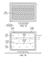
- FIG. 14 is a top-down view of a second embodiment of a die that employs centralized auxiliary minority carrier storage in accordance with a second novel aspect.
- FIG. 15 is a top-down diagram of the die of the second embodiment with no metallization, insulation, or passivation layers shown.
- FIG. 16 is a cross-sectional diagram of a mesa structure or a narrow strip structure of the second embodiment, where the mesa or narrow strip is relatively wide and has floating P+ type regions.
- FIGS. 17 and 18 are diagrams of a third embodiment.
- FIGS. 19 and 20 are diagrams of a fourth embodiment.
- FIGS. 21 and 22 are diagrams of a fifth embodiment.
- FIG. 23 is a flow chart of a method 200 in accordance with one novel aspect.
- FIG. 1 is a top-down diagram of a power diode integrated circuit die 1 in accordance with one novel aspect.
- the die 1 has a rectangular shape when considered from the illustrated top-down perspective.
- the peripheral edge portion of the upper surface of the die is covered with a rectangular ring 2 of a passivation layer as shown.
- the ring 2 of passivation may, for example, be a polyimide (also sometimes referred to as polymide or polymid) or a silicon nitride layer that is approximately 5-20 um polyimide or 0.5-2 um SIN thick.
- the central portion of the upper surface of the die has a covering metal anode electrode 3 .
- Metal anode electrode 3 may, for example, be an aluminum layer that is approximately 4 um thick.
- FIG. 2 is a diagram looking down onto the upper surface of the semiconductor material of the die 1 of FIG. 1 . Passivation, metallization and insulation layers are not shown in FIG. 2 so that the regions of semiconductor material can be shown.
- a specially-shaped P+ type anode region 4 extends 10 um down into an N ⁇ type layer 5 of N ⁇ type epitaxial silicon.
- a floating P+ type guard ring 6 extends around the periphery of the P+ type anode region 4 , and an N+ type channel stopper 7 at the peripheral upper edge of the die extends around the floating guard ring. There are six rectangular openings in the center portion of the P+ type anode region 4 .
- P+ type anode region 4 therefore has a mesh-shape that defines the two-dimensional array of openings.
- N ⁇ type semiconductor material of the underlying N ⁇ type layer 5 is illustrated in FIG. 2 extending up through the six openings in the mesh so that six mesa structures 8 - 13 of N ⁇ type semiconductor material are formed.
- Each of the six mesa structures 8 - 13 extends up to the planar upper semiconductor surface 15 of the die.
- Each of the six mesa structures 8 - 13 has a substantially rectangular planar surface in the plane of the upper surface 15 of the semiconductor material of the die.
- the N ⁇ type mesas are disposed in an array of rows and columns under a central area of the metal anode electrode 3 when the die is considered from a top-down perspective; there are relatively few N ⁇ type mesas in a peripheral area of the metal anode electrode (when the die is considered from the top-down perspective) and the peripheral area is more than two thirds as large as the central area.
- the density of N ⁇ type mesas is higher under this central third of the metal anode electrode than it is under the peripheral two-thirds of the metal anode electrode, in fact in the example of FIG. 2 all of the N ⁇ type mesas are disposed under the central third.
- FIG. 3 is a cross-sectional diagram taken along line A-A′ in FIG. 1 , for a simplified case in which there is only one guard ring.
- the innermost floating P+ type guard ring 6 is spaced about 90 um away from the outer peripheral edge of the P+ type anode region 4 .
- the distance between the anode region 4 and the first guard ring is empirically adjusted.
- the N ⁇ type layer 5 which is sometimes called a drift region, is a 60 um thick layer of epitaxially-grown silicon that was grown on N+ type substrate silicon layer 14 .
- N ⁇ type layer 5 is lightly doped to 28 ohm-cm.
- N+ type substrate layer 14 is 200 um thick in this example and is doped with phosphorus.
- the P+ type regions 4 and 6 and the N+ type channel stopper region 7 are formed down into the N ⁇ type layer 5 from the upper surface 15 of the semiconductor material.
- a layer of metal on the bottom surface of N+ type substrate layer 14 is a metal cathode electrode 16 . This metal cathode electrode 16 covers the entire bottom surface of the die 1 .
- a patterned feature 17 of a thin first dielectric layer covers the N ⁇ type material between the P+ type region 4 and the floating P+ guard ring 6 .
- Feature 18 is another feature of this first thin dielectric layer. Feature 18 extends around the periphery of the die and covers the inner part of the N+ type channel stopper 7 as shown.
- the thin dielectric layer may be a 0.5 to 2 um thick layer of thermal oxide, or glass, silicon nitride, or SIPOS (Semi-Insulating Polycrystalline Silicon).
- the thicker peripheral dielectric passivation layer may be a 5 to 20 um thick polyimide layer or 0.5 to 2 um silicon nitride or 0.2-0.5 um thick SIPOS.
- the thick passivation layer prevents arching of the field plate and prevents humidity from penetrating down into the top of the die.
- guard ring and associated floating field plate typically has several concentrically-oriented guard ring and field plate structures.
- the spacing between each pair of adjacent guard rings should be individually optimized.
- the guard ring and field plate structures can suffer from surface instabilities caused by high electric fields and passivation charges generated during processing.
- the surface charges can cause a variation in the surface potential and can create conducting surface channels on the lightly doped semiconductor metal between rings. This alters the potential sharing between rings and device breakdown can occur wherever there is excess charge due to increased electric fields.
- the field plate 19 reduces passivation charge.
- the N+ type channel stopper region 7 prevents the depletion region from the main PN junction of the device from reaching the edge of the die 1 under high voltage reverse bias conditions.
- the combination of the guard rings, the field plates, and the die electric layer 18 helps increase the blocking voltage the die can tolerate before suffering breakdown.
- FIG. 4 is a cross-sectional diagram taken along line B-B′ in FIG. 1 .
- FIG. 5 is a cross-sectional diagram taken along line C-C′ in FIG. 1 .
- Each of the mesa structures 8 - 13 of FIG. 2 is covered by a rectangular pad-like feature of the thin field dielectric layer.
- Pad feature 20 illustrated in FIG. 4 is the rectangular pad-like feature that covers mesa 8 .
- Pad feature 20 entirely covers the upper planar semiconductor surface of mesa structure 8 so that metal of metal anode electrode 3 does not contact any portion of the N ⁇ type semiconductor material of layer 5 .
- the top planar surface of the mesa structure 8 is a rectangular surface having a width of 140 microns and having a length of 1000 microns.
- the simplified top-down illustration of FIG. 2 that shows the mesas to be close to square is not to scale.
- FIG. 6 is a diagram that shows the doping profile extending into the semiconductor surface starting at a point on the upper semiconductor surface 15 on the surface of the P+ type region 4 .
- the P type dopant is boron.
- the N type dopant of the epitaxial layer 5 and of the substrate layer 14 is either phosphorus or arsenic.
- So-called “axial lifetime killers” are locally implanted to achieve an axial lifetime killer dose N ALK of about 2 ⁇ 10 12 recombination centers per square centimeter of silicon (denoted 2E12 cm ⁇ 2 ) at a depth of 8 um.
- the axial lifetime killer dopant that is implanted may, for example, be helium or protons.
- the axial life killers are locally implanted in the P+ type region 4 of the die to a depth of about 8 um, but are not implanted into the deep N ⁇ type material.
- FIG. 7 is a table that sets forth characteristics of the various parts of the power diode die 1 of FIGS. 1-5 .
- FIG. 8 is a diagram that illustrates minority carrier charge distribution at the main PN junction of the die 1 under forward bias conditions.
- the main PN junction is the junction between P+ type region 4 and N ⁇ type layer 5 .
- P NO is the background minority carrier concentration in the P+ type material on the left side of the PN junction.
- the minority carriers in the P+ type material are electrons, so the illustrated increasing concentration of charge carriers extending to the right in the diagram to the PN junction represents an increasing concentration of electrons.
- the silicon material is N ⁇ type material of layer 5 .
- N PO is the background minority carrier concentration in the N ⁇ type material on the right side of the PN junction.
- the minority carriers in the N ⁇ type material are holes, so the illustrated increasing concentration of charge carriers extending to the left in the diagram to the PN junction represents an increasing concentration of holes.
- the sum of the concentration of majority carriers and the concentration of minority carriers on one side of the PN junction matches the sum of the concentration of majority carriers and the concentration of minority carriers on other side. Due to the P type semiconductor material being more heavily doped with P type dopants than the N type semiconductor material is doped with N type dopants, P NO is lower than N PO . As is known in the art, a depletion region exists at the PN junction.
- This depletion region extends to the left into the P type material from the PN junction, and also extends to the right into the N type material from the PN junction. Conduction through the forward biased PN junction is primarily due to majority carriers. Holes pass from the left to right through the P type material on the left side of the PN junction and electrons pass from the right to the left through the N type material on the right side of the PN junction. This hole and electron flow constitutes the current flow through the PN junction structure.
- FIG. 9 is a diagram that illustrates minority carrier charge distribution at the PN junction under reverse bias conditions. Due to the reverse bias voltage, the depletion region is expanded both into the P type material from the PN junction as well as into the N type material from the PN junction. The increased reverse bias electric field across the PN junction sweeps minority carriers that are in the depletion region across the PN junction. For example, electrons that are minority carriers in the depletion region on the left side of the PN junction are moved under the force of the electric field to the right and so that they cross the PN junction. Similarly, holes that are minority carriers in the depletion region on the right side of the PN junction are moved under the force of the electric field in the opposite direction to the left so that they cross the PN junction. The result is the illustrated decreased concentration of minority carriers in the depletion region where the increased reverse bias electric field exists.
- FIG. 10 shows the result of this movement of minority carriers.
- the PN junction prior to time t 1 the PN junction is forward biased. A 0.7 forward voltage exists across the diode, and a forward current I F flows from the anode electrode to the cathode electrode. The magnitude of the forward current determines the number of charge carriers passing through the depletion region at the PN junction. The voltage across the PN junction is then switched from the forward voltage to a reverse voltage.
- a higher concentration of recombination centers in the semiconductor material therefore results in a corresponding higher rate of recombination.
- a lower concentration of recombination centers in the semiconductor material results in a corresponding lower rate of recombination.
- the reverse voltage across the PN junction increases. In the illustrated example, the PN junction is being used to block a reverse voltage of 400V. The reverse voltage across the PN junction is about 400V by time t 4 .
- the mesa structures 8 - 13 and the associated P+ type region 4 that has the six openings increase the amount of minority carriers stored in the center part of the diode die 1 .
- the N ⁇ type material of the mesa structures meets the P+ type semiconductor material of the P+ type region 4 and forms six vertically extending tubular PN junction extensions. These six vertically extending tubular PN junction extensions extend upward from the planar horizontally extending PN junction beneath the P+ type region 4 . During forward conduction, minority carriers are present in these six vertically extending tubular PN junction extensions.
- Reference numeral 32 in FIG. 10 identifies the exhibited reverse recovery current waveform of the novel diode die 1 of FIGS. 1-5 during a reverse recovery episode.
- Reference numeral 33 in FIG. 10 identifies the corresponding voltage across the novel diode die 1 of FIGS. 1-5 during the reverse recovery episode.
- the background concentration of recombination centers N ULC is increased to 2 ⁇ 10 12 recombination centers per cubic centimeter (denoted 2E12 cm ⁇ 3 ) as indicated in FIG. 6 .
- Charge carriers that recombine in the depletion region do not contribute to current conduction.
- the increase in recombination center concentration increases charge carrier recombination and is made to compensate for the increased amount of minority charge present in larger PN junction of the diode die. This allows the I RM of the novel diode die 1 to be the same as the conventional diode of waveforms 30 and 31 even though the novel die 1 has the six vertically extending tubular PN junction extensions.
- a function of axial lifetime killers (such as are created by Helium implantation or Proton implantation) is to reduce injection efficiency of holes into the N ⁇ during switching. The injection of holes contributes to the maximum reverse recovery current (I RM ).
- a function of uniform lifetime killers (such as are created by electron irradiation) is to reduce the t rr value.
- charge carriers diffuse from the die periphery (i.e. the passivation zone) to the center of the device and this movement of charge has a positive effect on soft recovery performance.
- the dopant concentrations and recombination center concentrations and mesa structure geometries are adjustable in an empirical manner to achieve the waveforms 32 and 33 of FIG. 10 .
- the novel diode die 1 has the same approximate I RM as the prior art diode, but the novel diode die 1 has a softer reverse recovery characteristic, without overshoot and without oscillation.
- the di/dt slope 26 during time t b in the novel diode die 1 is approximately 1000 A/us under the conditions of FIG.
- the novel diode die has a t rr of about 45 ns; whereas the di/dt slope 27 during time t b in the prior art diode is approximately 3000 A/us under the conditions of FIG. 10 and the prior art diode has a t rr of about 35 ns.
- the waveform diagram of FIG. 10 is not to scale.
- the 50 micron to 300 micron width of a mesa structure is, in one example, 140 microns and is just a wide enough separation that the lateral extending depletion regions of the PN junction on either side of the mesa extend inward and touch and merge at the rated reverse voltage of the diode.
- This mesa width generally is about twice the thickness of the N ⁇ type layer 5 .
- the 140 micron width of a mesa is 140/60 (2.33) times the 60 micron thickness of N ⁇ type layer 5 .
- the optimal width can also be empirically determined by making diodes with a range of mesa widths, and then testing the diodes to find the diode with the best performance.
- FIG. 11 is a table that sets forth a comparison of the novel diode die 1 of FIG. 1-5 to the prior art diode structure.
- the prior art diode structure being compared is of identical construction to the novel diode die 1 of FIG. 1-5 , except that the prior art diode structure does not have the novel mesa structures 8 - 13 and does not have the increased recombination center concentrations described above.
- FIG. 12 is a diagram that illustrates the movement of minority carriers during time t a in a peripheral area of the novel diode die 1 of FIGS. 1-5 . Note that the depletion region extends both laterally to the right as well as vertically down from the P+ type region 4 .
- FIG. 13 is a diagram that illustrates the movement of minority carriers during time t a in one of the mesa areas of the novel diode die 1 of FIGS. 1-5 . Note that there is a larger volume of depleted silicon in the mesa area as compared to other areas beneath the P+ type region 4 where there is no mesa and where the depletion region can only extend vertically downward from the P+ type region 4 . The increased amount of depleted silicon in the areas of the mesas 8 - 13 serves to balance the amount minority carriers present (at the time of switching) per unit area across the die.
- FIGS. 14 and 15 illustrate a second embodiment of novel diode die 1 .
- the second embodiment there are three P+ type regions 50 , 51 and 52 .
- the added minority charge storage areas at the center of the die are added by providing horizontally-extending narrow elongated strips 53 and 54 of the N ⁇ type material of layer 5 . These elongated strips extend through the center portion of the die.
- the elongated strips 53 and 54 of the N ⁇ type material of layer 5 extend up to the plane of the upper planar surface of the semiconductor portion of die 1 .
- a corresponding narrow strip of the third dielectric layer is disposed to cover each of the two narrow strips of N ⁇ type material so that the metal of the metal anode electrode 3 does not contact the N ⁇ type material of layer 5 in the narrow strip regions.
- the metal of the metal anode electrode 3 bridges over the narrow strip regions and makes contact with all three of the first, second and third P+ type regions 50 - 52 .
- forward current flows from the metal anode electrode 3 , in parallel through the three P+ type regions 50 - 52 , through the N ⁇ type epitaxial layer 5 , down through the N+ type substrate layer 14 , and to the metal cathode electrode 16 .
- Each narrow strip structure in the second embodiment may be considered a narrow and elongated mesa structure in that the narrow strip structure extends up to the plane of the upper surface of the semiconductor material and at that plane has an elongated strip-like planar surface.
- Regions of minority carrier charge storage beneath the metal cathode electrode can, for example, be provided using the structure shown in FIG. 16 .
- each mesa structure is 406 um wide.
- the structure of the diode die 1 in the example of FIG. 16 is otherwise the same as in the diode die of FIGS. 1-5 .
- each floating P+ type region 22 - 24 extend down from surface 15 into the N ⁇ type material of the mesa structure as shown.
- Each floating P+ type region is 2 um wide, and approximately 1000 um long, and is separated from another adjacent floating P+ type region or from an adjacent P+ type region 4 by 100 um of N ⁇ type semiconductor material of the N ⁇ type layer 5 .
- the gap 25 in the illustrated example is 406 um wide for a diode with a rate 200 ampere forward current, but in other examples the gap 25 may be made wider or narrower by providing more or fewer floating P+ type regions and/or by changing the dimensions and separations of the structures.
- the floating P+ type regions are not limited to the use in mesas per se, but rather also can be provided in the narrow strip embodiment of FIGS. 14 and 15 .
- the first and second narrow strips 53 and 54 are made wider (for example, 406 um).
- Parallel extending floating P+ type regions are formed to extend down into the N ⁇ type material of layer 5 in the area of each of these narrow strip regions.
- the floating P+ type regions are floating in that they are not electrically connected to any metal electrode or to the P+ type anode region 4 .
- FIGS. 17 and 18 are diagrams of a third embodiment in which there are island-shaped mesa structures, but the islands are of an elongated strip-like shape. In the embodiment of FIGS. 17 and 18 there is, however, only one P+ type anode region 4 , whereas in the embodiment of FIGS. 14 and 15 described above there are multiple P+ type regions.
- FIGS. 19 and 20 are diagrams of a fourth embodiment in which there are no mesa structures of upward extending N ⁇ type material as in the embodiment of FIGS. 1-5 , but rather there is a single P+ type anode region 4 with a planar bottom boundary. Where there are mesas in the embodiment of FIGS. 1-5 , however, in the fourth embodiment of FIGS. 19 and 20 there are areas at the upper semiconductor surface of the P+ type anode region 4 that do not make direct contact with the overlying metal anode electrode 3 (as shown) due to intervening pad features of the thin field dielectric layer. Pad feature 20 in FIGS. 19 and 20 is one such pad feature overlying one such minority carrier charge storage area. A minority carrier charge storage area exists under each such area where there is no direct contact between the metal anode electrode 3 and the semiconductor material of the P+ type region 4 .
- FIGS. 21 and 22 are diagrams of a fifth embodiment.
- the fifth embodiment is similar the fourth embodiment, except that metal of the metal anode electrode 3 does not extend over the minority carrier charge storage area. In one example there is also no pad feature 20 of the thin field dielectric layer disposed over the minority carrier charge storage area.
- FIG. 23 is a flowchart of a method 200 in accordance with one novel aspect.
- a P+ type region is formed into an upper surface of an N-type epitaxial silicon layer.
- the P+ type region has a plurality of centrally-located openings such that N ⁇ type semiconductor material from the N ⁇ type epitaxial layer extends up through each of the openings, thereby forming a plurality of N ⁇ type mesa structures.
- Each of the N ⁇ type mesa structures has a planar top surface disposed in the plane of the upper surface of the N ⁇ type epitaxial layer.
- the N ⁇ type epitaxial layer is disposed on an N+ type substrate layer.
- a plurality of features of an insulation layer are formed so that each respective one of the features covers a corresponding respective one of the mesa structures.
- a first metal electrode for example, an anode electrode
- a second metal electrode is formed on a bottom side of the N+ type substrate layer.
- a forward current can flow under a forward voltage condition from the first metal electrode to the second metal electrode.
- the diode blocks substantially all current from flowing in the reverse direction from the second metal electrode to the first metal electrode.
- the PN junction structure described above as having uniform minority charge carrier storage per unit area from its periphery to its center, is not limited to use in power diodes, but rather is also useful in other devices such as in an Insulated Gate Bipolar Transistor (IGBT), in a Field Effect Transistor (FET), in a Metal Oxide Semiconductor Field Effect Transistor (MOSFET), in a thyristor, and in a MOS Controlled Thyristor (MCT).
- IGBT Insulated Gate Bipolar Transistor
- FET Field Effect Transistor
- MOSFET Metal Oxide Semiconductor Field Effect Transistor
- MCT MOS Controlled Thyristor
- Different ones of the PN junction structures of the first through fifth embodiments may be used in various combinations on the same die. Accordingly, various modifications, adaptations, and combinations of various features of the described embodiments can be practiced without departing from the scope of the invention as set forth in the claims.
Landscapes
- Electrodes Of Semiconductors (AREA)
Abstract
Description
Claims (22)
Priority Applications (1)
| Application Number | Priority Date | Filing Date | Title |
|---|---|---|---|
| US13/783,134 US8836090B1 (en) | 2013-03-01 | 2013-03-01 | Fast recovery switching diode with carrier storage area |
Applications Claiming Priority (1)
| Application Number | Priority Date | Filing Date | Title |
|---|---|---|---|
| US13/783,134 US8836090B1 (en) | 2013-03-01 | 2013-03-01 | Fast recovery switching diode with carrier storage area |
Publications (2)
| Publication Number | Publication Date |
|---|---|
| US20140246761A1 US20140246761A1 (en) | 2014-09-04 |
| US8836090B1 true US8836090B1 (en) | 2014-09-16 |
Family
ID=51420578
Family Applications (1)
| Application Number | Title | Priority Date | Filing Date |
|---|---|---|---|
| US13/783,134 Active US8836090B1 (en) | 2013-03-01 | 2013-03-01 | Fast recovery switching diode with carrier storage area |
Country Status (1)
| Country | Link |
|---|---|
| US (1) | US8836090B1 (en) |
Cited By (1)
| Publication number | Priority date | Publication date | Assignee | Title |
|---|---|---|---|---|
| US20150016165A1 (en) * | 2013-03-15 | 2015-01-15 | David Schie | Gated thyristor power device |
Families Citing this family (10)
| Publication number | Priority date | Publication date | Assignee | Title |
|---|---|---|---|---|
| WO2013066959A1 (en) * | 2011-10-31 | 2013-05-10 | The Trustees Of Columbia University In The City Of New York | Systems and methods for imaging using single photon avalanche diodes |
| US9621864B2 (en) * | 2014-01-14 | 2017-04-11 | Microsoft Technology Licensing, Llc | Spectral imaging system |
| EP2996152B1 (en) * | 2014-09-15 | 2017-03-15 | ABB Schweiz AG | High frequency power diode and method for manufacturing the same |
| DE112015000206T5 (en) * | 2014-10-03 | 2016-08-25 | Fuji Electric Co., Ltd. | Semiconductor device and method of manufacturing a semiconductor device |
| US9704832B1 (en) | 2016-02-29 | 2017-07-11 | Ixys Corporation | Die stack assembly using an edge separation structure for connectivity through a die of the stack |
| CN106206754A (en) * | 2016-08-31 | 2016-12-07 | 吉林华微电子股份有限公司 | A kind of fast recovery diode improving recovery time and softness |
| US10424677B2 (en) * | 2017-08-31 | 2019-09-24 | Littelfuse, Inc. | Charge carrier extraction inverse diode |
| CN109755241B (en) * | 2017-11-01 | 2021-03-02 | 苏州东微半导体股份有限公司 | Power MOSFET device |
| US20230187435A1 (en) * | 2021-12-14 | 2023-06-15 | Skyworks Solutions, Inc. | Diode configuration for circuit protection |
| CN115295613B (en) * | 2022-10-08 | 2023-01-03 | 烟台台芯电子科技有限公司 | Fast recovery diode structure and manufacturing method thereof |
Citations (7)
| Publication number | Priority date | Publication date | Assignee | Title |
|---|---|---|---|---|
| US20030218220A1 (en) * | 2002-05-27 | 2003-11-27 | Mitsubishi Denki Kabushiki Kaisha | Power semiconductor device and method of manufacturing the same |
| US20050158979A1 (en) * | 2003-06-09 | 2005-07-21 | Seiji Momota | Method of manufacturing semiconductor device |
| US20060255379A1 (en) | 2005-05-12 | 2006-11-16 | Ixys Corporation | Stable diodes for low and high frequency applications |
| US20090160008A1 (en) * | 2007-12-25 | 2009-06-25 | Hirokazu Fujiwara | Semiconductor device and method of manufacturing the same |
| US20100025820A1 (en) * | 2008-07-29 | 2010-02-04 | Mitsubishi Electric Corporation | Semiconductor device |
| US8093652B2 (en) | 2002-08-28 | 2012-01-10 | Ixys Corporation | Breakdown voltage for power devices |
| US8153481B2 (en) | 2005-04-28 | 2012-04-10 | Ixys Corporation | Semiconductor power device with passivation layers |
-
2013
- 2013-03-01 US US13/783,134 patent/US8836090B1/en active Active
Patent Citations (7)
| Publication number | Priority date | Publication date | Assignee | Title |
|---|---|---|---|---|
| US20030218220A1 (en) * | 2002-05-27 | 2003-11-27 | Mitsubishi Denki Kabushiki Kaisha | Power semiconductor device and method of manufacturing the same |
| US8093652B2 (en) | 2002-08-28 | 2012-01-10 | Ixys Corporation | Breakdown voltage for power devices |
| US20050158979A1 (en) * | 2003-06-09 | 2005-07-21 | Seiji Momota | Method of manufacturing semiconductor device |
| US8153481B2 (en) | 2005-04-28 | 2012-04-10 | Ixys Corporation | Semiconductor power device with passivation layers |
| US20060255379A1 (en) | 2005-05-12 | 2006-11-16 | Ixys Corporation | Stable diodes for low and high frequency applications |
| US20090160008A1 (en) * | 2007-12-25 | 2009-06-25 | Hirokazu Fujiwara | Semiconductor device and method of manufacturing the same |
| US20100025820A1 (en) * | 2008-07-29 | 2010-02-04 | Mitsubishi Electric Corporation | Semiconductor device |
Cited By (2)
| Publication number | Priority date | Publication date | Assignee | Title |
|---|---|---|---|---|
| US20150016165A1 (en) * | 2013-03-15 | 2015-01-15 | David Schie | Gated thyristor power device |
| US9142657B2 (en) * | 2013-03-15 | 2015-09-22 | David Schie | Gated thyristor power device |
Also Published As
| Publication number | Publication date |
|---|---|
| US20140246761A1 (en) | 2014-09-04 |
Similar Documents
| Publication | Publication Date | Title |
|---|---|---|
| US8836090B1 (en) | Fast recovery switching diode with carrier storage area | |
| US10950717B2 (en) | Semiconductor device having semiconductor regions with an impurity concentration distribution which decreases from a respective peak toward different semiconductor layers | |
| JP6050891B2 (en) | Semiconductor device with junction termination extension | |
| US9064923B2 (en) | Bipolar semiconductor component with a fully depletable channel zone | |
| JP2019179922A (en) | Semiconductor device, and circuit for controlling field effect transistor of semiconductor device | |
| US20170294526A1 (en) | Reverse-conducting semiconductor device | |
| US11948976B2 (en) | Vertical MOSFET having trench gate structure containing silicon carbide | |
| KR20140015412A (en) | Semiconductor devices including schottky diodes having overlapping doped regions and methods of fabricating same | |
| JP2022059487A (en) | Semiconductor device | |
| US9385223B2 (en) | Reverse-conducting power semiconductor device | |
| CN102468298A (en) | Accumulator Field Effect Transistor with Integrated Clamp Circuit | |
| US20240162295A1 (en) | Gate-commuted thyristor cell with a base region having a varying thickness | |
| CN116093152A (en) | Semiconductor device | |
| WO2019053199A1 (en) | A concept for silicon carbide power devices | |
| JP2016167597A (en) | Semiconductor device with trench/barrier schottky diode | |
| US12176423B2 (en) | FinFET power semiconductor devices | |
| JP6799515B2 (en) | Semiconductor device | |
| JP7213398B2 (en) | insulated gate bipolar transistor | |
| US12426349B2 (en) | Reverse conducting power semiconductor device and method for manufacturing the same | |
| US10483384B2 (en) | Transistor device with high current robustness | |
| EP1276156A1 (en) | High power bipolar transistor | |
| US12513928B2 (en) | Bidirectional thyristor device | |
| EP3935671B1 (en) | Semiconductor device with gradual injection of charge carriers for softer reverse recovery | |
| JP2022059446A (en) | Semiconductor device | |
| US20120217539A1 (en) | Semiconductor Component with Improved Dynamic Behavior |
Legal Events
| Date | Code | Title | Description |
|---|---|---|---|
| AS | Assignment |
Owner name: IXYS CORPORATION, CALIFORNIA Free format text: ASSIGNMENT OF ASSIGNORS INTEREST;ASSIGNOR:VEERAMMA, SUBHAS CHANDRA BOSE JAYAPPA;REEL/FRAME:029909/0735 Effective date: 20130205 |
|
| STCF | Information on status: patent grant |
Free format text: PATENTED CASE |
|
| MAFP | Maintenance fee payment |
Free format text: PAYMENT OF MAINTENANCE FEE, 4TH YEAR, LARGE ENTITY (ORIGINAL EVENT CODE: M1551) Year of fee payment: 4 |
|
| AS | Assignment |
Owner name: IXYS, LLC, CALIFORNIA Free format text: MERGER AND CHANGE OF NAME;ASSIGNORS:IXYS CORPORATION;IXYS, LLC;REEL/FRAME:045406/0656 Effective date: 20180116 |
|
| AS | Assignment |
Owner name: LITTELFUSE, INC., ILLINOIS Free format text: ASSIGNMENT OF ASSIGNORS INTEREST;ASSIGNOR:IXYS, LLC;REEL/FRAME:049056/0649 Effective date: 20190430 |
|
| MAFP | Maintenance fee payment |
Free format text: PAYMENT OF MAINTENANCE FEE, 8TH YEAR, LARGE ENTITY (ORIGINAL EVENT CODE: M1552); ENTITY STATUS OF PATENT OWNER: LARGE ENTITY Year of fee payment: 8 |