US8830631B2 - Features for write fringing reduction - Google Patents
Features for write fringing reduction Download PDFInfo
- Publication number
- US8830631B2 US8830631B2 US13/914,990 US201313914990A US8830631B2 US 8830631 B2 US8830631 B2 US 8830631B2 US 201313914990 A US201313914990 A US 201313914990A US 8830631 B2 US8830631 B2 US 8830631B2
- Authority
- US
- United States
- Prior art keywords
- layer
- ferromagnetic
- tracks
- soft underlayer
- data layer
- Prior art date
- Legal status (The legal status is an assumption and is not a legal conclusion. Google has not performed a legal analysis and makes no representation as to the accuracy of the status listed.)
- Expired - Fee Related
Links
- 230000009467 reduction Effects 0.000 title description 2
- 230000004907 flux Effects 0.000 claims abstract description 18
- 230000008878 coupling Effects 0.000 claims abstract description 9
- 238000010168 coupling process Methods 0.000 claims abstract description 9
- 238000005859 coupling reaction Methods 0.000 claims abstract description 9
- 239000003302 ferromagnetic material Substances 0.000 claims abstract description 8
- 230000005290 antiferromagnetic effect Effects 0.000 claims abstract description 7
- 239000010410 layer Substances 0.000 claims description 113
- 230000005294 ferromagnetic effect Effects 0.000 claims description 41
- 230000005415 magnetization Effects 0.000 claims description 15
- OKTJSMMVPCPJKN-UHFFFAOYSA-N Carbon Chemical compound [C] OKTJSMMVPCPJKN-UHFFFAOYSA-N 0.000 claims description 12
- 229910052799 carbon Inorganic materials 0.000 claims description 12
- KJTLSVCANCCWHF-UHFFFAOYSA-N Ruthenium Chemical compound [Ru] KJTLSVCANCCWHF-UHFFFAOYSA-N 0.000 claims description 10
- 229910052707 ruthenium Inorganic materials 0.000 claims description 10
- 239000011229 interlayer Substances 0.000 claims description 5
- 230000005291 magnetic effect Effects 0.000 abstract description 28
- 238000013461 design Methods 0.000 abstract description 7
- 238000004519 manufacturing process Methods 0.000 abstract description 7
- 239000000696 magnetic material Substances 0.000 abstract description 5
- 239000000463 material Substances 0.000 abstract description 5
- 238000000992 sputter etching Methods 0.000 abstract description 5
- 230000008021 deposition Effects 0.000 abstract description 4
- 230000000694 effects Effects 0.000 abstract description 2
- 229910001423 beryllium ion Inorganic materials 0.000 abstract 1
- 239000004926 polymethyl methacrylate Substances 0.000 description 18
- 238000000034 method Methods 0.000 description 15
- 238000007737 ion beam deposition Methods 0.000 description 7
- 230000008901 benefit Effects 0.000 description 4
- 229910001030 Iron–nickel alloy Inorganic materials 0.000 description 3
- 150000002500 ions Chemical class 0.000 description 3
- 239000002904 solvent Substances 0.000 description 3
- CSCPPACGZOOCGX-UHFFFAOYSA-N Acetone Chemical compound CC(C)=O CSCPPACGZOOCGX-UHFFFAOYSA-N 0.000 description 2
- 239000002245 particle Substances 0.000 description 2
- 230000008569 process Effects 0.000 description 2
- XLYOFNOQVPJJNP-UHFFFAOYSA-N water Substances O XLYOFNOQVPJJNP-UHFFFAOYSA-N 0.000 description 2
- VYZAMTAEIAYCRO-UHFFFAOYSA-N Chromium Chemical compound [Cr] VYZAMTAEIAYCRO-UHFFFAOYSA-N 0.000 description 1
- 229910000531 Co alloy Inorganic materials 0.000 description 1
- 229910003321 CoFe Inorganic materials 0.000 description 1
- RYGMFSIKBFXOCR-UHFFFAOYSA-N Copper Chemical compound [Cu] RYGMFSIKBFXOCR-UHFFFAOYSA-N 0.000 description 1
- 101000606504 Drosophila melanogaster Tyrosine-protein kinase-like otk Proteins 0.000 description 1
- LFQSCWFLJHTTHZ-UHFFFAOYSA-N Ethanol Chemical compound CCO LFQSCWFLJHTTHZ-UHFFFAOYSA-N 0.000 description 1
- 229910001362 Ta alloys Inorganic materials 0.000 description 1
- QCWXUUIWCKQGHC-UHFFFAOYSA-N Zirconium Chemical compound [Zr] QCWXUUIWCKQGHC-UHFFFAOYSA-N 0.000 description 1
- FKZMGPZJGLFUBV-UHFFFAOYSA-N [Cr].[Ru] Chemical compound [Cr].[Ru] FKZMGPZJGLFUBV-UHFFFAOYSA-N 0.000 description 1
- 229910045601 alloy Inorganic materials 0.000 description 1
- 239000000956 alloy Substances 0.000 description 1
- 229910052804 chromium Inorganic materials 0.000 description 1
- 239000011651 chromium Substances 0.000 description 1
- 238000004140 cleaning Methods 0.000 description 1
- 229910052802 copper Inorganic materials 0.000 description 1
- 239000010949 copper Substances 0.000 description 1
- 238000005260 corrosion Methods 0.000 description 1
- 230000007797 corrosion Effects 0.000 description 1
- 230000007423 decrease Effects 0.000 description 1
- 230000005347 demagnetization Effects 0.000 description 1
- 238000001514 detection method Methods 0.000 description 1
- 239000012467 final product Substances 0.000 description 1
- 238000010884 ion-beam technique Methods 0.000 description 1
- 230000005381 magnetic domain Effects 0.000 description 1
- 238000004949 mass spectrometry Methods 0.000 description 1
- 238000012986 modification Methods 0.000 description 1
- 230000004048 modification Effects 0.000 description 1
- 239000011368 organic material Substances 0.000 description 1
- 238000000059 patterning Methods 0.000 description 1
- 238000012545 processing Methods 0.000 description 1
- 239000000047 product Substances 0.000 description 1
- 230000001105 regulatory effect Effects 0.000 description 1
- 239000007787 solid Substances 0.000 description 1
- 238000003860 storage Methods 0.000 description 1
- GUVRBAGPIYLISA-UHFFFAOYSA-N tantalum atom Chemical compound [Ta] GUVRBAGPIYLISA-UHFFFAOYSA-N 0.000 description 1
- 238000012360 testing method Methods 0.000 description 1
- 238000011144 upstream manufacturing Methods 0.000 description 1
- 229910052726 zirconium Inorganic materials 0.000 description 1
Images


Classifications
-
- G—PHYSICS
- G11—INFORMATION STORAGE
- G11B—INFORMATION STORAGE BASED ON RELATIVE MOVEMENT BETWEEN RECORD CARRIER AND TRANSDUCER
- G11B5/00—Recording by magnetisation or demagnetisation of a record carrier; Reproducing by magnetic means; Record carriers therefor
- G11B5/62—Record carriers characterised by the selection of the material
- G11B5/64—Record carriers characterised by the selection of the material comprising only the magnetic material without bonding agent
- G11B5/66—Record carriers characterised by the selection of the material comprising only the magnetic material without bonding agent the record carriers consisting of several layers
- G11B5/676—Record carriers characterised by the selection of the material comprising only the magnetic material without bonding agent the record carriers consisting of several layers having magnetic layers separated by a nonmagnetic layer, e.g. antiferromagnetic layer, Cu layer or coupling layer
-
- G—PHYSICS
- G11—INFORMATION STORAGE
- G11B—INFORMATION STORAGE BASED ON RELATIVE MOVEMENT BETWEEN RECORD CARRIER AND TRANSDUCER
- G11B5/00—Recording by magnetisation or demagnetisation of a record carrier; Reproducing by magnetic means; Record carriers therefor
- G11B5/62—Record carriers characterised by the selection of the material
- G11B5/64—Record carriers characterised by the selection of the material comprising only the magnetic material without bonding agent
- G11B5/66—Record carriers characterised by the selection of the material comprising only the magnetic material without bonding agent the record carriers consisting of several layers
- G11B5/667—Record carriers characterised by the selection of the material comprising only the magnetic material without bonding agent the record carriers consisting of several layers including a soft magnetic layer
-
- G—PHYSICS
- G11—INFORMATION STORAGE
- G11B—INFORMATION STORAGE BASED ON RELATIVE MOVEMENT BETWEEN RECORD CARRIER AND TRANSDUCER
- G11B5/00—Recording by magnetisation or demagnetisation of a record carrier; Reproducing by magnetic means; Record carriers therefor
- G11B5/74—Record carriers characterised by the form, e.g. sheet shaped to wrap around a drum
- G11B5/82—Disk carriers
-
- G—PHYSICS
- G11—INFORMATION STORAGE
- G11B—INFORMATION STORAGE BASED ON RELATIVE MOVEMENT BETWEEN RECORD CARRIER AND TRANSDUCER
- G11B5/00—Recording by magnetisation or demagnetisation of a record carrier; Reproducing by magnetic means; Record carriers therefor
- G11B5/84—Processes or apparatus specially adapted for manufacturing record carriers
- G11B5/855—Coating only part of a support with a magnetic layer
Definitions
- the present invention is related to magnetic recording systems, and in particular, to write fringing reduction in discrete track recording.
- PMR perpendicular magnetic recording
- a further way to increase bit density is to employ discrete track recording (DTR).
- DTR discrete track recording
- magnetic information is stored on single tracks in the media as opposed to storing the information in a bit patterned media.
- adjacent tracks are physically separated by air gaps in the form of grooves. These air gaps are minimized to increase the bit density such that tracks are placed closer together for a high track per inch (TPI) configuration allowing a high bits per square inch count in the media.
- TPI track per inch
- MWW magnetic write width
- OVW overwrite
- the magnetic write width of the head should be as close to the width of the track as possible, however, there still exists a tendency to have some of the field extend outwardly from the head and reach into the adjacent track. Such a field is known as a fringe field.
- the fringing magnetic flux can travel into the adjacent track leading to adjacent track erasure.
- the head field in the off-track direction is found to decay slowly. This slow decay is disadvantageous because it adds to further adjacent track erasure as the fringe field decays. It has been challenging to address this problem because the size of the write head, the amount of the fringe field, the fly height of the head, and the interlayer thicknesses in the media are parameters that are involved in the phenomenon, however, such parameters are essentially set and cannot be readily changed. For example, it is unlikely that the head (and therefore the MWW) could be narrowed readily, without the loss of OVW.
- the DTR media of the present invention includes ferromagnetic islands that are disposed in the air gap grooves between tracks. The ferromagnetic islands act to conduct the write fringing magnetic flux into the soft underlayer of the media to thereby reduce the risk of adjacent track erasure.
- a ferromagnetic island is located within each groove between tracks in the media.
- the island is flush or slightly recessed from the top recording layer of a magnetic recording disk.
- the bottom of the islands are located adjacent to the bottom of the recording layer.
- the magnetic properties of the ferromagnetic islands are selected to conduct the fringe field flux directly downwardly into the soft underlayer of the media. This technique minimizes the loss of on-track write field and minimizes the strength of erase field in adjacent tracks.
- a method of manufacturing the DTR media is also provided in accordance with the present invention. Briefly, a special layered mask is used to create trenches between tracks in the media data layer. Ion milling techniques are used to remove remaining data layer material. Ion beam deposition (IBD) steps are used to place the layers forming the ferromagnetic islands within the trenches, as described further herein.
- IBD Ion beam deposition
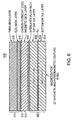
- FIG. 1 is a schematic illustration of a typical DTR/PMR media design in accordance with the prior art
- FIG. 2 is a schematic illustration showing media with ferromagnetic islands between tracks in accordance with an illustrative embodiment of the present invention
- FIG. 3A is a schematic illustration of the magnetic write pole and its location with respect to the tracks and islands of the present invention.
- FIG. 3B is the media of FIG. 3A showing the magnetic flux lines with respect to the components
- FIG. 4 is a side elevation of the ferromagnetic island of the present invention illustrating the rest state magnetization coupling within the layers of the island;
- FIGS. 5A and 5B illustrate a flow chart of a procedure in accordance with a method of manufacturing the media in accordance with the present invention
- FIG. 6 is a schematic illustration of the pre-manufacture layering, which results in improved media of the present invention.
- FIG. 7 illustrates the patterning after the application of the nano-imprint mask used in the second step of the method of manufacture of the present invention
- FIG. 8 is a schematic illustration of the ion milling step after undercutting the PMMA mask by dissolving part of a B 2 O 3 layer;
- FIG. 9 is an illustration of the deposition of the soft magnetic material forming a layer of the island in accordance with the present invention.
- FIG. 10 illustrates the deposition of the final carbon overcoat after mask lift-off, and cleaning steps.
- FIG. 1 illustrates a cross section of a prior art DTR disk media 100 .
- the disk media 100 contains discrete tracks 102 through 108 which comprise the recording layer of the disk media.
- the discrete tracks 102 through 108 are the data layer in which the information is stored on the disk, i.e. these tracks contain the domains that are magnetically adjusted when writing data onto the disk and which are analyzed to read information from the disk.
- a soft underlayer 110 may be comprised of an alloy of cobalt/tantalum/zirconium (CoTaZr) and Ruthenium (Ru).
- CoTaZr cobalt/tantalum/zirconium
- Ru Ruthenium
- FIG. 2 illustrates the disk media 200 , which is a discrete track recording media suitable for perpendicular magnetic recording.
- the discrete tracks 202 , 204 , 206 and 208 are located above the soft underlayer 210 .
- soft magnetic regions such as ferromagnetic islands 222 , 224 and 226 are located between the tracks as shown in FIG. 2 .
- the ferromagnetic islands are comprised of, illustratively, a soft magnetic material which will be described further herein.
- FIG. 3A depicts one embodiment of the invention and illustrates several geometric parameters of the design.
- the disk media 300 has discrete recording tracks 301 , 303 and 305 , which make up a recording layer 306 .
- This recording layer is located above the soft underlayer 310 .
- the top surface of the recording layer is identified by reference character 312 and the bottom surface of the recording layer is identified by reference character 314 .
- a magnetic write pole 320 is writes data onto the media 300 .
- a ferromagnetic island 304 for example, can be flush with or slightly recessed from the top of the recording layer 312 .
- the bottom of the ferromagnetic island 304 for example, in accordance with the invention, is relocated generally at the bottom of the recording layer, as illustrated by 314 .
- the width of the ferromagnetic islands (W) is preferably a fraction of the track pitch (TP), and TP is defined as WW+W (with reference to the illustration of FIG. 3A ).
- the distance from the pole head to the island 302 is defined as D2.
- D1 is the distance from the bottom of the island 302 , for example, to the top of the soft underlayer 310
- DSUL is the distance from the pole head to the top of the soft underlayer 310 .
- the islands can have a trapezoidal cross sectional shape, as illustrated in phantom by the item 330 .
- the saturation magnetization of the island should be selected to avoid early saturation in accordance with the invention.
- FIG. 3B illustrates the magnetic flux lines for the disk media 300 when flux is emanating from write pole 320 .
- the magnetic flux from the write pole 320 which is writing on the track 303 is illustrated by the arrow 402 .
- the write pole 320 also generates fringe fields 404 and 406 .
- the fringe fields 404 and 406 are absorbed by the islands 302 and 304 of the present invention.
- the paths 408 and 410 show that the flux is conducted directly to the soft underlayer 310 during a write operation.
- FIG. 4 illustrates a ferromagnetic island 400 in accordance with the present invention.
- the magnetic flux 402 travels from the write pole 320 to the disk in, for example, a “Z” direction as shown in FIG. 4 .
- the ferromagnetic islands of the present invention thus provide a path to magnetic ground (in the SUL).
- the ferromagnetic coupling of the ferromagnetic island 400 should be such as that shown in FIG. 4 .
- the rest state magnetization in the upper layer 420 is oriented in a first direction, and the rest state magnetization in the lower layer 422 is radiating in an opposite direction.
- the procedure 500 begins at step 502 and continues to step 504 in which a B 2 O 3 mask layer and a PMMA mask layer are placed over a set of layers for a perpendicular recording medium.
- the media 600 includes a soft underlayer 602 , which is comprised of a bottom layer 604 , a ruthenium intermediate layer 606 , and a top SUL layer 608 .
- the SUL is biased in such a manner that the rest state magnetization in the bottom layer 604 is in a direction opposite to that of the top layer 608 .
- Above the SUL is an interlayer of ruthenium or ruthenium chromium 610 .
- the magnetic data layer 612 is comprised primarily of magnetic material. Above the magnetic data layer is a carbon overcoat layer 613 .
- a two layer mask is provided over the carbon overcoat layer 613 .
- the two layer mask 614 is comprised of a top layer of a soft organic material such as poly-methyl methacrylate (PMMA) that is illustratively cured at elevated temperatures to improve its resistance to solvents.
- PMMA poly-methyl methacrylate
- a harder bottom layer is disposed adjacent to the PMMA layer. This harder bottom layer is, illustratively, substantially comprised of B 2 O 3 .
- B 2 O 3 mask layer is illustrated in FIG. 6 as layer 616 and the PMMA mask layer is illustrated in FIG. 6 as the layer 618 .
- step 506 in which a nano imprint mask is pressed into the PMMA layer 618 .
- This step is illustrated in FIG. 7 , which is a portion of the media of FIG. 6 , and depicts the SUL 602 , the intermediate layer 610 , the magnetic data layer 612 and the carbon overcoat layer 613 , the B 2 O 3 layer 616 and the PMMA layer 618 .
- a nano-imprint mask 702 is pressed down into the PMMA layer 618 .
- the nano imprint mask in pressed into the layer 618 of PMMA, but not far into the harder B 2 O 3 layer 616 . This squeezes portions of the PMMA layer to form trenches with almost no PMMA layer therebetween.
- the nano-imprint mask 702 is removed in accordance with step 508 and the trenches are first exposed to a mild ion mill step to remove PMMA residues from the trenches and are then exposed water to partially dissolve the B 2 O 3 layer 616 .
- a mild ion mill step to remove PMMA residues from the trenches and are then exposed water to partially dissolve the B 2 O 3 layer 616 .
- FIG. 8 the nano imprint mask has been removed and the PMMA has been squeezed to leave trenches such as the trenches 802 , 804 and 806 .
- the PMMA layer is now formed of separate structures, such as structures 810 , 811 .
- the B 2 O 3 layer 616 When the B 2 O 3 layer 616 is exposed to water, it is done in such a manner that some of it partly dissolves but not all of it so that an overhang, such as the overhang 812 on the structure 810 , is left.
- the overhang 812 is intentionally left on each of the PMMA structures so that the milled data layer material will not redeposit in a way that bridges the overhang.
- step 510 ion milling is used to remove the data layer to create a cavity that reaches down to the interlayer which, as noted, is between the data layer and the SUL.
- the depth of this ion milling step can be regulated using end point detection of the RU atoms (e.g. mass spectrometry).
- end point detection of the RU atoms e.g. mass spectrometry.
- some material from the milled data layer is re-deposited such as that illustrated by 814 and 816 onto the overhang 812 on each PMMA structure.
- an ion beam deposition (IBD) process is used to create the first layer of the ferromagnetic island in accordance with the present invention. More specifically, referring to FIG. 9 , an ion beam deposition is performed at normal incidence from a soft ferromagnetic target, which may be CoFe, NiFe, CoTaZr or CoNiFe. Illustratively, a nickel iron alloy is used in the example of FIG. 9 . More specifically, a NiFe target 902 is bombarded with ions, resulting in ion beam deposition 904 of the first layer 906 of the ferromagnetic island 912 .
- a soft ferromagnetic target which may be CoFe, NiFe, CoTaZr or CoNiFe.
- a nickel iron alloy is used in the example of FIG. 9 . More specifically, a NiFe target 902 is bombarded with ions, resulting in ion beam deposition 904 of the first layer 906 of the ferrom
- this layer is illustratively approximately half that of the magnetically hard data layer 614 .
- the intermediate layer of the island is ion beam deposited.
- This intermediate layer 908 is an antiferromagnetic coupling layer.
- Antiferromagnetic layer 908 may consist of ruthenium, copper or chromium. If the layer 908 is substantially comprised of ruthenium, its thickness is, illustratively, about 7 angstroms. This achieves the desired anti ferromagnetic behavior.
- the final layer of the island is a ferromagnetic layer 910 , which is deposited from the same target as the first or from a third target with the same or different alloy.
- its magnetization times its thickness product should be approximately equal to that of the first layer 906 , so that most of the remnant flux can circulate between the two layers, as noted hereinbefore. This avoids demagnetization fields within the ferromagnetic island itself, which could undesirably travel into an adjacent layer.
- the soft antiferromagnetic coupling nature of the island of the present invention is similar to the magnetic coupling of the SUL 602 that exists within the media.
- the total thicknesses of the three deposited layers should not exceed the depth of the circumferential cavities that were previously milled into the disk.
- the trench should be substantially filled with the layered materials, but not to a level higher than the data layer on the discrete track. This is to maintain a consistent flyable height, thereby avoiding peaks and valleys being created on the surface of the media.
- a carbon overcoat layer is then placed on the final product, as shown in FIG. 5B in step 520 .
- the mask is lifted off, and a solvent is used to remove the remaining B 2 O 3 layer 616 .
- the mask will be stripped from the disk using exposure to a suitable sequence of solvents, such as acetone, to strip the PMMA and alcohol to strip the remaining B 2 O 3 .
- a suitable sequence of solvents such as acetone
- Application of a high pressure blast of solid carbon particles will aid in the removal of any adhered particles.
- a final carbon layer 1010 is deposited to improve corrosion resistance and mechanical durability by covering areas where the carbon deposition was too thin at the edge of the mask openings. This is step 523 in FIG. 5B .
- the disk will go through a standard burnish and test processing as will be understood by those skilled in the art as a clean up step 524 .
- the top layer of the media can be fully or partially laminated, if desired, in a particular application of the invention.
- the procedure ends at step 526 .
- the present invention provides an improved media design and a method of manufacturing such a media that reduces the effects of write fringing.
- the ferromagnetic island is disposed between tracks in a discrete track recording media. This design has the advantage that the island reduces the loss of flux out of the write head field, but yet reduces the risk of adjacent track data erasure. This is accomplished without requiring additional components to be added to the write head.
Landscapes
- Magnetic Record Carriers (AREA)
- Manufacturing Of Magnetic Record Carriers (AREA)
Abstract
Description
-
- W>10% TP and W<45% TP
Claims (20)
Priority Applications (1)
| Application Number | Priority Date | Filing Date | Title |
|---|---|---|---|
| US13/914,990 US8830631B2 (en) | 2005-11-03 | 2013-06-11 | Features for write fringing reduction |
Applications Claiming Priority (5)
| Application Number | Priority Date | Filing Date | Title |
|---|---|---|---|
| US73324705P | 2005-11-03 | 2005-11-03 | |
| US11/592,507 US7876529B1 (en) | 2005-11-03 | 2006-11-03 | Recording disk with antiferromagnetically coupled multilayer ferromagnetic island disposed in trench between discrete tracks |
| US12/967,927 US8243389B2 (en) | 2005-11-03 | 2010-12-14 | Write fringing reduction for recording media |
| US13/585,625 US8462463B2 (en) | 2005-11-03 | 2012-08-14 | Write fringing reduction for recording media |
| US13/914,990 US8830631B2 (en) | 2005-11-03 | 2013-06-11 | Features for write fringing reduction |
Related Parent Applications (1)
| Application Number | Title | Priority Date | Filing Date |
|---|---|---|---|
| US13/585,625 Continuation US8462463B2 (en) | 2005-11-03 | 2012-08-14 | Write fringing reduction for recording media |
Publications (2)
| Publication Number | Publication Date |
|---|---|
| US20130271873A1 US20130271873A1 (en) | 2013-10-17 |
| US8830631B2 true US8830631B2 (en) | 2014-09-09 |
Family
ID=43479798
Family Applications (4)
| Application Number | Title | Priority Date | Filing Date |
|---|---|---|---|
| US11/592,507 Expired - Fee Related US7876529B1 (en) | 2005-11-03 | 2006-11-03 | Recording disk with antiferromagnetically coupled multilayer ferromagnetic island disposed in trench between discrete tracks |
| US12/967,927 Expired - Fee Related US8243389B2 (en) | 2005-11-03 | 2010-12-14 | Write fringing reduction for recording media |
| US13/585,625 Expired - Fee Related US8462463B2 (en) | 2005-11-03 | 2012-08-14 | Write fringing reduction for recording media |
| US13/914,990 Expired - Fee Related US8830631B2 (en) | 2005-11-03 | 2013-06-11 | Features for write fringing reduction |
Family Applications Before (3)
| Application Number | Title | Priority Date | Filing Date |
|---|---|---|---|
| US11/592,507 Expired - Fee Related US7876529B1 (en) | 2005-11-03 | 2006-11-03 | Recording disk with antiferromagnetically coupled multilayer ferromagnetic island disposed in trench between discrete tracks |
| US12/967,927 Expired - Fee Related US8243389B2 (en) | 2005-11-03 | 2010-12-14 | Write fringing reduction for recording media |
| US13/585,625 Expired - Fee Related US8462463B2 (en) | 2005-11-03 | 2012-08-14 | Write fringing reduction for recording media |
Country Status (1)
| Country | Link |
|---|---|
| US (4) | US7876529B1 (en) |
Families Citing this family (5)
| Publication number | Priority date | Publication date | Assignee | Title |
|---|---|---|---|---|
| US7876529B1 (en) | 2005-11-03 | 2011-01-25 | Seagate Technology Llc | Recording disk with antiferromagnetically coupled multilayer ferromagnetic island disposed in trench between discrete tracks |
| US8679860B1 (en) * | 2006-08-07 | 2014-03-25 | Sandia Corporation | Lateral electrodeposition of compositionally modulated metal layers |
| US8771848B2 (en) * | 2006-10-10 | 2014-07-08 | Seagate Technology Llc | Bit patterned magnetic media |
| JP2012212488A (en) * | 2011-03-30 | 2012-11-01 | Toshiba Corp | Information recording device and information recording method |
| US9190093B2 (en) | 2013-02-06 | 2015-11-17 | HGST Netherlands, B.V. | Reduced adjacent track errors in bit-patterned media |
Citations (37)
| Publication number | Priority date | Publication date | Assignee | Title |
|---|---|---|---|---|
| USRE33949E (en) | 1985-01-22 | 1992-06-02 | Digital Equipment Corporation | Vertical magnetic recording arrangement |
| US5568331A (en) | 1989-10-27 | 1996-10-22 | Hitachi, Ltd. | Method of head positioning and magnetic recording disk drive using the same |
| US5956216A (en) | 1995-05-24 | 1999-09-21 | Regents Of The University Of Minnesota | Magnetic storage having discrete elements with quantized magnetic moments |
| US6014296A (en) | 1995-07-24 | 2000-01-11 | Kabushiki Kaisha Toshiba | Magnetic disk, method of manufacturing magnetic disk and magnetic recording apparatus |
| US20020034666A1 (en) | 2000-09-07 | 2002-03-21 | Kiely James Dillon | Magnetic recording medium utilizing patterned nanoparticle arrays |
| US6391430B1 (en) * | 2000-06-21 | 2002-05-21 | International Business Machines Corporation | Patterned magnetic recording media with discrete magnetic regions separated by regions of antiferromagnetically coupled films |
| US20020136927A1 (en) | 2001-03-22 | 2002-09-26 | Hiroyuki Hieda | Recording medium, method of manufacturing recording medium and recording apparatus |
| US20020142192A1 (en) | 2001-03-30 | 2002-10-03 | Kabushiki Kaisha Toshiba | Method of patterning magnetic products using chemical reactions |
| US6576113B1 (en) | 1999-10-29 | 2003-06-10 | California Institute Of Technology | Method of electroplating of high aspect ratio metal structures into semiconductors |
| US20030179481A1 (en) | 2001-02-16 | 2003-09-25 | Mcneil Michael | Patterned medium |
| US6643082B1 (en) | 1999-06-08 | 2003-11-04 | Seagate Technology Llc | Servo sector format for a patterned media |
| US6660357B1 (en) | 2000-02-04 | 2003-12-09 | Seagate Technology Llc | Perpendicular magnetic recording media with laminated soft magnetic underlayer |
| US20030234470A1 (en) | 2002-06-20 | 2003-12-25 | Haan Stephen F. | Embossing apparatus, method of use thereof and resulting article |
| US6723450B2 (en) * | 2002-03-19 | 2004-04-20 | Hitachi Global Storage Technologies Netherlands B.V. | Magnetic recording medium with antiparallel coupled ferromagnetic films as the recording layer |
| US6738207B1 (en) | 1999-08-18 | 2004-05-18 | Seagate Technology Llc | Method for synchronizing the write current for magnetic recording with the bit islands on discrete bit patterned media |
| US20040101713A1 (en) | 2002-11-27 | 2004-05-27 | Wachenschwanz David E. | Perpendicular magnetic discrete track recording disk |
| US20040131890A1 (en) | 2002-09-27 | 2004-07-08 | Akira Kikitsu | Perpendicular magnetic recording medium |
| US6770386B1 (en) * | 1999-09-02 | 2004-08-03 | Fujitsu Limited | Magnetic recording medium and its manufacturing method |
| US6773834B2 (en) * | 1999-10-08 | 2004-08-10 | Hitachi Global Storage Technologies Netherlands B.V. | Laminated magnetic recording media with antiferromagnetically coupled layer as one of the individual magnetic layers in the laminate |
| US20040166372A1 (en) | 2003-02-24 | 2004-08-26 | Chiseki Haginoya | Magnetic recording media and method of forming them |
| US20040174636A1 (en) | 2003-03-05 | 2004-09-09 | Shoji Suzuki | Magnetic recording disk having a transition zone |
| US6842313B1 (en) | 2002-04-08 | 2005-01-11 | Maxtor Corporation | Floating down stream perpendicular write head shield |
| US20050036223A1 (en) | 2002-11-27 | 2005-02-17 | Wachenschwanz David E. | Magnetic discrete track recording disk |
| US6890667B1 (en) | 2001-11-09 | 2005-05-10 | Maxtor Corporation | Soft underlayer structure for magnetic recording |
| US20050122609A1 (en) | 2003-12-03 | 2005-06-09 | Manfred Albrecht | Patterned multilevel perpendicular magnetic recording media |
| US20050122612A1 (en) | 2003-12-03 | 2005-06-09 | Manfred Albrecht | Magnetic recording system with patterned multilevel perpendicular magnetic recording |
| US20050134992A1 (en) | 2003-12-19 | 2005-06-23 | Homola Andrew M. | Magnetic recording disk having DTR patterned CSS zone |
| US20050146992A1 (en) * | 2004-01-05 | 2005-07-07 | Fujitsu Limited | Magnetic recording medium, magnetic storage and method for reproducing information from magnetic recording medium |
| US20050157597A1 (en) | 2003-05-29 | 2005-07-21 | Seagate Technology Llc | Optimized media grain packing fraction for bit patterned magnetic recording media |
| US20050190478A1 (en) | 2004-03-01 | 2005-09-01 | Hsiao Wenchien D. | Longitudinal magnetic recording using magnetic media with a soft underlayer |
| US20060139799A1 (en) | 2004-12-28 | 2006-06-29 | Seagate Technology Llc | Granular perpendicular magnetic recording media with dual recording layer and method of fabricating same |
| US20060228586A1 (en) * | 2005-04-06 | 2006-10-12 | Seagate Technology Llc | Ferromagnetically coupled magnetic recording media |
| US20060269799A1 (en) * | 2005-05-24 | 2006-11-30 | Do Hoa V | Perpendicular magnetic recording disk with improved recording layer having high oxygen content |
| US20060269792A1 (en) * | 2005-05-24 | 2006-11-30 | Fullerton Eric E | Perpendicular magnetic recording medium with improved antiferromagnetically-coupled recording layer |
| US20070020486A1 (en) * | 2005-07-19 | 2007-01-25 | Berger Andreas K | Perpendicular magnetic recording medium with metamagnetic antiferromagnetically-coupled layer between the soft underlayer and recording layer |
| US20070037016A1 (en) * | 2005-08-12 | 2007-02-15 | Do Hoa V | Perpendicular magnetic recording disk with recording layer containing selected metal oxides and formed on a reduced-thickness exchange-break layer |
| US7876529B1 (en) | 2005-11-03 | 2011-01-25 | Seagate Technology Llc | Recording disk with antiferromagnetically coupled multilayer ferromagnetic island disposed in trench between discrete tracks |
-
2006
- 2006-11-03 US US11/592,507 patent/US7876529B1/en not_active Expired - Fee Related
-
2010
- 2010-12-14 US US12/967,927 patent/US8243389B2/en not_active Expired - Fee Related
-
2012
- 2012-08-14 US US13/585,625 patent/US8462463B2/en not_active Expired - Fee Related
-
2013
- 2013-06-11 US US13/914,990 patent/US8830631B2/en not_active Expired - Fee Related
Patent Citations (42)
| Publication number | Priority date | Publication date | Assignee | Title |
|---|---|---|---|---|
| USRE33949E (en) | 1985-01-22 | 1992-06-02 | Digital Equipment Corporation | Vertical magnetic recording arrangement |
| US5568331A (en) | 1989-10-27 | 1996-10-22 | Hitachi, Ltd. | Method of head positioning and magnetic recording disk drive using the same |
| US5956216A (en) | 1995-05-24 | 1999-09-21 | Regents Of The University Of Minnesota | Magnetic storage having discrete elements with quantized magnetic moments |
| US6014296A (en) | 1995-07-24 | 2000-01-11 | Kabushiki Kaisha Toshiba | Magnetic disk, method of manufacturing magnetic disk and magnetic recording apparatus |
| US6643082B1 (en) | 1999-06-08 | 2003-11-04 | Seagate Technology Llc | Servo sector format for a patterned media |
| US6738207B1 (en) | 1999-08-18 | 2004-05-18 | Seagate Technology Llc | Method for synchronizing the write current for magnetic recording with the bit islands on discrete bit patterned media |
| US6770386B1 (en) * | 1999-09-02 | 2004-08-03 | Fujitsu Limited | Magnetic recording medium and its manufacturing method |
| US6773834B2 (en) * | 1999-10-08 | 2004-08-10 | Hitachi Global Storage Technologies Netherlands B.V. | Laminated magnetic recording media with antiferromagnetically coupled layer as one of the individual magnetic layers in the laminate |
| US6576113B1 (en) | 1999-10-29 | 2003-06-10 | California Institute Of Technology | Method of electroplating of high aspect ratio metal structures into semiconductors |
| US6660357B1 (en) | 2000-02-04 | 2003-12-09 | Seagate Technology Llc | Perpendicular magnetic recording media with laminated soft magnetic underlayer |
| US6391430B1 (en) * | 2000-06-21 | 2002-05-21 | International Business Machines Corporation | Patterned magnetic recording media with discrete magnetic regions separated by regions of antiferromagnetically coupled films |
| US20020034666A1 (en) | 2000-09-07 | 2002-03-21 | Kiely James Dillon | Magnetic recording medium utilizing patterned nanoparticle arrays |
| US20030179481A1 (en) | 2001-02-16 | 2003-09-25 | Mcneil Michael | Patterned medium |
| US20020136927A1 (en) | 2001-03-22 | 2002-09-26 | Hiroyuki Hieda | Recording medium, method of manufacturing recording medium and recording apparatus |
| US20020142192A1 (en) | 2001-03-30 | 2002-10-03 | Kabushiki Kaisha Toshiba | Method of patterning magnetic products using chemical reactions |
| US20040191557A1 (en) | 2001-03-30 | 2004-09-30 | Kabushiki Kaisha Toshiba | Method of patterning magnetic products using chemical reaction |
| US20040258833A1 (en) | 2001-03-30 | 2004-12-23 | Kabushiki Kaisha Toshiba | Method of patterning magnetic products using chemical reaction |
| US6890667B1 (en) | 2001-11-09 | 2005-05-10 | Maxtor Corporation | Soft underlayer structure for magnetic recording |
| US6723450B2 (en) * | 2002-03-19 | 2004-04-20 | Hitachi Global Storage Technologies Netherlands B.V. | Magnetic recording medium with antiparallel coupled ferromagnetic films as the recording layer |
| US6842313B1 (en) | 2002-04-08 | 2005-01-11 | Maxtor Corporation | Floating down stream perpendicular write head shield |
| US20030234470A1 (en) | 2002-06-20 | 2003-12-25 | Haan Stephen F. | Embossing apparatus, method of use thereof and resulting article |
| US20040131890A1 (en) | 2002-09-27 | 2004-07-08 | Akira Kikitsu | Perpendicular magnetic recording medium |
| US20040101713A1 (en) | 2002-11-27 | 2004-05-27 | Wachenschwanz David E. | Perpendicular magnetic discrete track recording disk |
| US20050036223A1 (en) | 2002-11-27 | 2005-02-17 | Wachenschwanz David E. | Magnetic discrete track recording disk |
| US20040166372A1 (en) | 2003-02-24 | 2004-08-26 | Chiseki Haginoya | Magnetic recording media and method of forming them |
| US20040174636A1 (en) | 2003-03-05 | 2004-09-09 | Shoji Suzuki | Magnetic recording disk having a transition zone |
| US20050157597A1 (en) | 2003-05-29 | 2005-07-21 | Seagate Technology Llc | Optimized media grain packing fraction for bit patterned magnetic recording media |
| US20050122609A1 (en) | 2003-12-03 | 2005-06-09 | Manfred Albrecht | Patterned multilevel perpendicular magnetic recording media |
| US20050122612A1 (en) | 2003-12-03 | 2005-06-09 | Manfred Albrecht | Magnetic recording system with patterned multilevel perpendicular magnetic recording |
| US6947235B2 (en) | 2003-12-03 | 2005-09-20 | Hitachi Global Storage Technologies Netherlands B.V. | Patterned multilevel perpendicular magnetic recording media |
| US20050134992A1 (en) | 2003-12-19 | 2005-06-23 | Homola Andrew M. | Magnetic recording disk having DTR patterned CSS zone |
| US20050146992A1 (en) * | 2004-01-05 | 2005-07-07 | Fujitsu Limited | Magnetic recording medium, magnetic storage and method for reproducing information from magnetic recording medium |
| US20050190478A1 (en) | 2004-03-01 | 2005-09-01 | Hsiao Wenchien D. | Longitudinal magnetic recording using magnetic media with a soft underlayer |
| US20060139799A1 (en) | 2004-12-28 | 2006-06-29 | Seagate Technology Llc | Granular perpendicular magnetic recording media with dual recording layer and method of fabricating same |
| US20060228586A1 (en) * | 2005-04-06 | 2006-10-12 | Seagate Technology Llc | Ferromagnetically coupled magnetic recording media |
| US20060269799A1 (en) * | 2005-05-24 | 2006-11-30 | Do Hoa V | Perpendicular magnetic recording disk with improved recording layer having high oxygen content |
| US20060269792A1 (en) * | 2005-05-24 | 2006-11-30 | Fullerton Eric E | Perpendicular magnetic recording medium with improved antiferromagnetically-coupled recording layer |
| US20070020486A1 (en) * | 2005-07-19 | 2007-01-25 | Berger Andreas K | Perpendicular magnetic recording medium with metamagnetic antiferromagnetically-coupled layer between the soft underlayer and recording layer |
| US20070037016A1 (en) * | 2005-08-12 | 2007-02-15 | Do Hoa V | Perpendicular magnetic recording disk with recording layer containing selected metal oxides and formed on a reduced-thickness exchange-break layer |
| US7876529B1 (en) | 2005-11-03 | 2011-01-25 | Seagate Technology Llc | Recording disk with antiferromagnetically coupled multilayer ferromagnetic island disposed in trench between discrete tracks |
| US8243389B2 (en) | 2005-11-03 | 2012-08-14 | Seagate Technology Llc | Write fringing reduction for recording media |
| US8462463B2 (en) | 2005-11-03 | 2013-06-11 | Seagate Technology Llc | Write fringing reduction for recording media |
Non-Patent Citations (5)
| Title |
|---|
| "What is DTR?", Komag, Inc., http://www.komag.com/technology/dtr-what.html, copyright Komag Inc., Nov. 30, 2005, p. 1. |
| "What is DTR?", Komag, Inc., http://www.komag.com/technology/dtr—what.html, copyright Komag Inc., Nov. 30, 2005, p. 1. |
| File History for U.S. Appl. No. 11/592,507. |
| File History for U.S. Appl. No. 12/967,927. |
| File History for U.S. Appl. No. 13/585,625. |
Also Published As
| Publication number | Publication date |
|---|---|
| US20110085267A1 (en) | 2011-04-14 |
| US8243389B2 (en) | 2012-08-14 |
| US20120327536A1 (en) | 2012-12-27 |
| US7876529B1 (en) | 2011-01-25 |
| US20130271873A1 (en) | 2013-10-17 |
| US8462463B2 (en) | 2013-06-11 |
Similar Documents
| Publication | Publication Date | Title |
|---|---|---|
| US7969684B2 (en) | Write head design and method for reducing adjacent track interference at very narrow track widths | |
| US6703099B2 (en) | Perpendicular magnetic recording media with patterned soft magnetic underlayer | |
| US8110085B2 (en) | Assisted deposition, narrow trench damascene process for manufacturing a write pole of a magnetic write head | |
| US20060093863A1 (en) | Magnetic recording medium, manufacturing process thereof, and magnetic recording apparatus | |
| US20070247746A1 (en) | Perpendicular magnetic recording write head with notched trailing shield and method for making | |
| US8830631B2 (en) | Features for write fringing reduction | |
| US7359146B2 (en) | Perpendicular magnetic recording element having stacked FM and AFM films applying magnetic bias along easy axis of soft magnetic film | |
| US20070211380A1 (en) | Perpendicular magnetic head | |
| US20100155363A1 (en) | Method for manufacturing a magnetic write head having a write pole with a trailing edge taper using a rieable hard mask | |
| US9536548B1 (en) | Magnetic write head with novel hot seed design to mitigate adjacent track interference | |
| JP2007220208A (en) | Magnetic head, magnetic recording and reproducing device, and method for manufacturing magnetic head | |
| US7145750B2 (en) | Perpendicular magnetic recording head and perpendicular magnetic recording and reproducing system | |
| US20100155364A1 (en) | Magnetic write head having a stepped trailing shield and write pole with a sloped trailing edge | |
| JP4468439B2 (en) | Method for manufacturing magnetic recording medium | |
| US7497008B2 (en) | Method of fabricating a thin film magnetic sensor on a wafer | |
| US10699733B1 (en) | Write head with reduced side to trailing shield spacing | |
| US8040633B2 (en) | Magnetic head and magnetic recording-reproducing apparatus | |
| JP2005174449A (en) | Vertical magnetic recording element, thin film magnetic head, magnetic head device, and magnetic recording/reproducing device | |
| US20100155232A1 (en) | Method for manufacturing a magnetic write head having a write pole trailing edge taper | |
| WO2009147729A1 (en) | Magnetic head and its manufacturing method | |
| CN101241704B (en) | Magnetic disk device | |
| US7500302B2 (en) | Process for fabricating a magnetic recording head with a laminated write gap | |
| US6462916B1 (en) | Magnetic disc apparatus | |
| US7500303B2 (en) | Method of fabricating a magnetic sensor on a wafer | |
| US7536774B2 (en) | Method and apparatus for integrating a stair notch and a gap bump at a pole tip in a write head |
Legal Events
| Date | Code | Title | Description |
|---|---|---|---|
| AS | Assignment |
Owner name: SEAGATE TECHNOLOGY LLC, CALIFORNIA Free format text: ASSIGNMENT OF ASSIGNORS INTEREST;ASSIGNORS:BENAKLI, MOURAD;MALLARY, MICHAEL;SIGNING DATES FROM 20070116 TO 20070212;REEL/FRAME:031260/0861 |
|
| FEPP | Fee payment procedure |
Free format text: MAINTENANCE FEE REMINDER MAILED (ORIGINAL EVENT CODE: REM.) |
|
| LAPS | Lapse for failure to pay maintenance fees |
Free format text: PATENT EXPIRED FOR FAILURE TO PAY MAINTENANCE FEES (ORIGINAL EVENT CODE: EXP.); ENTITY STATUS OF PATENT OWNER: LARGE ENTITY |
|
| STCH | Information on status: patent discontinuation |
Free format text: PATENT EXPIRED DUE TO NONPAYMENT OF MAINTENANCE FEES UNDER 37 CFR 1.362 |
|
| FP | Lapsed due to failure to pay maintenance fee |
Effective date: 20180909 |