US8827459B2 - Optical unit - Google Patents
Optical unit Download PDFInfo
- Publication number
- US8827459B2 US8827459B2 US14/013,493 US201314013493A US8827459B2 US 8827459 B2 US8827459 B2 US 8827459B2 US 201314013493 A US201314013493 A US 201314013493A US 8827459 B2 US8827459 B2 US 8827459B2
- Authority
- US
- United States
- Prior art keywords
- light
- optical
- optical unit
- beam spot
- screen
- Prior art date
- Legal status (The legal status is an assumption and is not a legal conclusion. Google has not performed a legal analysis and makes no representation as to the accuracy of the status listed.)
- Active
Links
Images


Classifications
-
- G—PHYSICS
- G09—EDUCATION; CRYPTOGRAPHY; DISPLAY; ADVERTISING; SEALS
- G09G—ARRANGEMENTS OR CIRCUITS FOR CONTROL OF INDICATING DEVICES USING STATIC MEANS TO PRESENT VARIABLE INFORMATION
- G09G3/00—Control arrangements or circuits, of interest only in connection with visual indicators other than cathode-ray tubes
- G09G3/02—Control arrangements or circuits, of interest only in connection with visual indicators other than cathode-ray tubes by tracing or scanning a light beam on a screen
-
- G—PHYSICS
- G02—OPTICS
- G02B—OPTICAL ELEMENTS, SYSTEMS OR APPARATUS
- G02B27/00—Optical systems or apparatus not provided for by any of the groups G02B1/00 - G02B26/00, G02B30/00
- G02B27/10—Beam splitting or combining systems
- G02B27/1006—Beam splitting or combining systems for splitting or combining different wavelengths
- G02B27/102—Beam splitting or combining systems for splitting or combining different wavelengths for generating a colour image from monochromatic image signal sources
- G02B27/104—Beam splitting or combining systems for splitting or combining different wavelengths for generating a colour image from monochromatic image signal sources for use with scanning systems
-
- G—PHYSICS
- G02—OPTICS
- G02B—OPTICAL ELEMENTS, SYSTEMS OR APPARATUS
- G02B27/00—Optical systems or apparatus not provided for by any of the groups G02B1/00 - G02B26/00, G02B30/00
- G02B27/09—Beam shaping, e.g. changing the cross-sectional area, not otherwise provided for
-
- G—PHYSICS
- G02—OPTICS
- G02B—OPTICAL ELEMENTS, SYSTEMS OR APPARATUS
- G02B27/00—Optical systems or apparatus not provided for by any of the groups G02B1/00 - G02B26/00, G02B30/00
- G02B27/10—Beam splitting or combining systems
- G02B27/14—Beam splitting or combining systems operating by reflection only
- G02B27/145—Beam splitting or combining systems operating by reflection only having sequential partially reflecting surfaces
-
- G—PHYSICS
- G03—PHOTOGRAPHY; CINEMATOGRAPHY; ANALOGOUS TECHNIQUES USING WAVES OTHER THAN OPTICAL WAVES; ELECTROGRAPHY; HOLOGRAPHY
- G03B—APPARATUS OR ARRANGEMENTS FOR TAKING PHOTOGRAPHS OR FOR PROJECTING OR VIEWING THEM; APPARATUS OR ARRANGEMENTS EMPLOYING ANALOGOUS TECHNIQUES USING WAVES OTHER THAN OPTICAL WAVES; ACCESSORIES THEREFOR
- G03B21/00—Projectors or projection-type viewers; Accessories therefor
- G03B21/14—Details
- G03B21/20—Lamp housings
- G03B21/2006—Lamp housings characterised by the light source
- G03B21/2013—Plural light sources
-
- H—ELECTRICITY
- H04—ELECTRIC COMMUNICATION TECHNIQUE
- H04N—PICTORIAL COMMUNICATION, e.g. TELEVISION
- H04N9/00—Details of colour television systems
- H04N9/12—Picture reproducers
- H04N9/31—Projection devices for colour picture display, e.g. using electronic spatial light modulators [ESLM]
- H04N9/3129—Projection devices for colour picture display, e.g. using electronic spatial light modulators [ESLM] scanning a light beam on the display screen
-
- H—ELECTRICITY
- H04—ELECTRIC COMMUNICATION TECHNIQUE
- H04N—PICTORIAL COMMUNICATION, e.g. TELEVISION
- H04N9/00—Details of colour television systems
- H04N9/12—Picture reproducers
- H04N9/31—Projection devices for colour picture display, e.g. using electronic spatial light modulators [ESLM]
- H04N9/3141—Constructional details thereof
- H04N9/315—Modulator illumination systems
- H04N9/3155—Modulator illumination systems for controlling the light source
-
- H—ELECTRICITY
- H04—ELECTRIC COMMUNICATION TECHNIQUE
- H04N—PICTORIAL COMMUNICATION, e.g. TELEVISION
- H04N9/00—Details of colour television systems
- H04N9/12—Picture reproducers
- H04N9/31—Projection devices for colour picture display, e.g. using electronic spatial light modulators [ESLM]
- H04N9/3141—Constructional details thereof
- H04N9/315—Modulator illumination systems
- H04N9/3164—Modulator illumination systems using multiple light sources
Definitions
- the present invention relates to an image display device that displays an image by scanning a screen with an optical beam of a light source after modulation of the beam according to a particular level of an image signal. More particularly, the invention relates to miniaturizing an optical unit.
- the new types of displays such as a DMD (Digital Mirror Device) type, liquid-crystal panel type, or optical scanning type display, which employ lasers or LEDs as light sources, are coming into existence to construct a large screen with a compact image-display device design.
- a white light source for example, allows the volume of the light source to be reduced remarkably and thus the image display device to be dimensionally reduced.
- a monochromatic light source of, for example, red (R), green (G), and blue (B), further allows finer-image formation in addition to miniaturization.
- JP-A-2007-293226 discloses a laser display device that comprises focusing means including a plurality of laser diode elements each emitting laser light and scanning means for reflecting the laser light so that an image is projected onto a screen.
- the conventional device that uses the technique disclosed in JP-A-2007-293226, however, is expensive since the plurality of laser light sources are arranged proximately.
- the conventional device has another problem in that since a large amount of heat occurs, optical axes of the light sources become misaligned and/or optical output intensity decreases.
- the device further presents the problem of degradation in resolution due to variations in beam spot sizes of the multiple lasers.
- an object of the present invention is to provide: an optical unit that is simpler in structure, less expensive, and capable of offering higher-resolution image quality while reducing device dimensions and weight; and an image display device using the optical unit.
- an optical unit comprises one or a plurality of light sources, one or a plurality of optical elements each controlling a spread of light, a combining element that combines optical beams emitted from each light source, and a scanning element; wherein the light source outputs an optical beam that will generate an elliptically shaped beam spot on the screen, the beam spot having a major axis substantially perpendicular to a scanning direction.
- the present invention makes achievable a compact optical unit capable of providing high-resolution image quality, and an image display device using the optical unit.
- FIG. 1A schematically shows a configuration of an optical unit according to a first embodiment of the present invention
- FIG. 1B shows a beam spot formed on a screen during projection by an image display device using the optical unit of the present invention
- FIG. 1C shows beam spots formed on a screen, and luminous intensity levels obtained, during projection using a conventional driving method
- FIG. 1D shows beam spots formed on the screen, and luminous intensity levels obtained, during projection by the image display device using the optical unit of the present invention
- FIG. 2 schematically shows a configuration of an optical unit according to a second embodiment of the present invention
- FIG. 3 schematically shows a configuration of an optical unit according to a third embodiment of the present invention.
- FIG. 4 schematically shows a configuration of an optical unit according to a fourth embodiment of the present invention.
- FIG. 5 schematically shows a configuration of an optical unit according to a fifth embodiment of the present invention.
- FIG. 6 schematically shows a configuration of an optical unit according to a sixth embodiment of the present invention.
- FIG. 7A is a diagram that shows a light source and optical element of the optical unit of the present invention, and a screen;
- FIG. 7B is a diagram that shows the screen onto which an image is projected by the image display device using the optical unit of the present invention, and pixels in a scanning direction on the screen;
- FIG. 7C is a diagram that shows one pixel on the screen and one beam spot formed thereon during projection by the image display device using the optical unit of the present invention
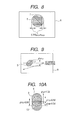
- FIG. 8 is another diagram that shows one pixel on the screen and one beam spot formed thereon during projection by the image display device using the optical unit of the present invention
- FIG. 9 is yet another diagram that shows a white beam formed on the screen during projection using the optical unit of the present invention.
- FIG. 10A is a further diagram that shows beam spots formed on the screen during projection by the image display device using the optical unit of the present invention.
- FIG. 10B is a further diagram that shows beam spots formed on the screen during projection by the image display device using the optical unit of the present invention.
- FIG. 11 schematically shows a configuration of an optical unit according to a seventh embodiment of the present invention.
- FIG. 12 schematically shows a configuration of an optical unit according to an eighth embodiment of the present invention.
- FIG. 13A is a diagram that schematically shows an example of time-varying changes in optical output level that are observed when the optical unit of the present invention is driven;
- FIG. 13B is a diagram showing an example of a conventional driving method (PWM driving).
- FIG. 13C is a diagram showing another example of a conventional driving method (analog driving).
- FIG. 14 schematically shows a configuration of an optical unit according to a ninth embodiment of the present invention.
- FIG. 15 is a diagram that shows an embodiment of an image display device.
- FIG. 1A schematically shows a configuration of an optical unit according to a first embodiment of the present invention.
- the optical unit 12 according to the present embodiment includes a plurality of light sources 1 a , 1 b , and 1 c , a plurality of optical elements 2 a , 2 b , and 2 c that each control a spread of light, an element 3 that combines the lights emitted from the light sources, and a scanning element 4 .
- the light from each of the light sources 1 a , 1 b , and 1 c generates an elliptically shaped spot, a major axis of which is nearly perpendicular to a scanning direction as shown in FIG. 1B .
- a color combiner 3 such as a color-combining mirror, prism, light guide, or optical fiber, will be used as the combining element 3 .
- Timing of activation of the light sources can be controlled in the scanning direction, so a shift in color can be prevented from occurring, but the control is difficult in a direction perpendicular to the scanning direction.
- the present invention has an advantage in that since spots can be disposed to be elongate with respect to the scanning direction, even if spots of different colors shift in position, overlapping area sizes of the spots will be large enough to prevent optical-axis misalignment and color shifting.
- FIG. 1C shows beam spots formed on a screen, and luminous intensity levels obtained, during projection using a conventional driving method.
- the fact that sizes of the beam spots for one pixel are nearly equal to one another and adjacent pixels are too dark has blurred the image, making high-resolution sharp image display difficult.
- images are displayed at high resolution since, as shown in FIG. 1D , minor axes of the spots are short for one pixel, and thus since the light sources 1 a , 1 b , and 1 c can be deactivated before the spots enter a next pixel.
- the light sources 1 a , 1 b , and 1 c here are of a laser type, electric power can be saved by stopping the laser oscillations during a black-color display period, since laser light can be modulated according to a particular image signal level.
- the light sources 1 a , 1 b , and 1 c are secured using an ultraviolet (UV) curing resin or fixed by engagement.
- UV ultraviolet
- the optical elements 2 a , 2 b , and 2 c are disposed at immediate rear of the light sources.
- Shapes of the lenses in this case are convex, concave, spherical, or non-spherical. Cylindrical lenses may be disposed to shape the beams emitted from the light sources. The shaping allows incidence of the beams appropriately shaped according to a shape of a reflecting portion formed as part of the scanning element 4 , and high efficiency is therefore obtained. At the same time, increases in temperature due to protrusion of any beams from the reflecting portion are suppressed.
- the optical elements 2 a , 2 b , and 2 c may be disposed immediately at rear of structures of the light sources 1 a , 1 b , and 1 c , or alternatively the former may be disposed near the light-emitting points inside the structures.
- the disposition near the light-emitting points makes the optical elements 2 a , 2 b , and 2 c acquire light more efficiently, as well as allowing generation of smaller spots on the screen 6 and hence, further improvement of image quality.
- the present embodiment assumes spot diameters of 1 mm or less on the reflecting portion of the scanning element 4 .
- An actuator or a feedback sensor may be mounted such that the positions of the optical elements 2 a , 2 b , and 2 c are automatically controllable according to the optical-axes of the light-emitting points of the light sources 1 a , 1 b , and 1 c . This prevents the misalignment of the optical axes and provides high resolution.
- the light sources 1 a , 1 b , and 1 c used can be white or each can be of either a three-color type including R (red), G (green), and B (blue), or a four-color type including R (red), G 1 (green 1 ), G 2 (green 2 ), and B (blue), or including R (red), G (green), B (blue), and Y (yellow).
- White light sources 1 a , 1 b , and 1 c enhance luminance.
- Monochromatic light sources 1 a , 1 b , and 1 c of the three-color or four-color types significantly improve color reproducibility, enhancing image quality.
- a plurality of light sources 1 a , 1 b , and 1 c that are 2 to 5 nanometers different from one another in wavelength may be used. This allows reduction of, for example, a speckle pattern caused by interference if laser light sources 1 a , 1 b , and 1 c are used.
- LEDs or lasers are used as the light sources 1 a , 1 b , and 1 c , and a dichroic mirror or a dichroic prism is used as the combining element 3 , it suffices just to obtain optical characteristics of its dichroic surface in a wavelength region enabling the light sources 1 a , 1 b , and 1 c to exhibit at least 10% of peak intensity on beam profiles (laser light intensity distribution diagrams) of the light sources.
- the LED or laser light sources 1 a , 1 b , and 1 c have a peaked light-emission distribution, not a broad one, it suffices just to obtain a transmittance/reflectance of at least 94%, as one optical characteristic of the dichroic surface, in a range of approximately +/ ⁇ 10 nm of a peak wavelength. For this reason, the number of layers on the dichroic surface can be reduced and thus the optical unit can be manufactured at a lower cost.
- the plurality of light sources 1 a , 1 b , and 1 c may be mounted in independent packages or in one package. Additionally, either the color-combining element 3 or the scanning element 4 may be mounted, with the light sources 1 a , 1 b , and 1 c , in one package. Mounting in independent packages offers advantages in that heat becomes easy to release and in that the light sources 1 a , 1 b , and 1 c elude a peak wavelength drift and an optical loss. Meanwhile, mounting in one package is advantageous in that using monochromatic light sources 1 a , 1 b , 1 c renders both color combination and optical axis alignment easy.
- the scanning element 4 may include one two-dimensional scanning member or two one-dimensional scanning members.
- the present embodiment assumes that the reflecting portion of the scanning element 4 has either a round, elliptical, square, or rectangular shape.
- the present embodiment also assumes that the reflecting portion is a maximum of 1 mm in size. Making the reflecting portion have a shape that fits the shape of the beam emitted from each of the light sources 1 a , 1 b , and 1 c , and have a minimum size, weight can be reduced and a driving speed of the optical unit can be correspondingly increased for finer image quality.
- the reflecting portion of the scanning element 4 uses, for example, an aluminum- or silver-deposited or dielectric, multilayered film, as its material. This material may be top-coated with SiO 2 , TiO 2 , or the like. Provided that a reflectance of at least 90% is obtained in the wavelength region that enables at least 10% of the peak intensity to be achieved on the beam profiles of the light sources 1 a , 1 b , and 1 c , high-luminance images can be obtained and the amount of heat generated by the scanning element 4 can be reduced. The optical unit 12 can therefore be enhanced in efficiency.
- Beams of either a round, elliptical, square, or rectangular shape will then be acquirable.
- any scattered beams that may have impinged upon, for example, a torsion bar or the like, except at the reflecting portion of the scanning element 4 can be removed for finer spots.
- the aperture 44 has an oblique cross-section, which may look like a stairway. This is effective for preventing diffracted light from occurring.
- the aperture is black in color, and is manufactured by, for example, alumite machining of a metal such as aluminum.
- An elongated hole for mounting the aperture 44 is provided in a bottom portion of the housing 444 in order to retain the aperture accurately in the x direction in the FIG. 1A . Accordingly, even if the light sources 1 a , 1 b , and 1 c , the combining element 3 , or other elements are disposed askew, the position of the aperture 44 can be adjusted to suit the optical axes, so that high-resolution spots with minimum flare can be obtained.
- the housing 444 is formed from a metal such as aluminum, and is easy to work at a low cost. Hold members of the light sources 1 a , 1 b , and 1 c , optical elements 2 a , 2 b , and 2 c , and combining element 3 , are independent of one another, each including a heat-releasing member. Thus, even if the light sources 1 a , 1 b , and 1 c each send off a large amount of heat, the heat can be released from the light sources 1 a , 1 b , and 1 c , without damaging the optical elements 2 a , 2 b , and 2 c and the combining element 3 .
- higher image quality can be obtained by preventing the occurrence of a peak wavelength drift, an optical output loss, and shifts in the positions of the light-emitting points.
- the optical unit 12 of the present invention is mounted in a motor vehicle or a mobile phone and an ambient temperature of the optical unit 12 exceeds a specified range of the light sources 1 a , 1 b , and 1 c , temperatures of the light sources can be lowered to stay within their guaranteed operating temperature ranges, such that high luminance can be obtained.
- a cushioning material may be disposed inside the housing 444 to enhance its impact resistance.
- the housing 444 has an elongate hole in a holding position of the scanning element 4 . This makes the scanning element 4 adjustable in the x direction in the FIG. 1A so that beams enter the scanning element 4 without loss, even if the light sources 1 a , 1 b , and 1 c and/or the combining element 3 are disposed askew. The occurrence of heat can thus be suppressed.
- FIG. 2 schematically shows a configuration of an optical unit according to a second embodiment of the present invention.
- the combining element 3 in the optical unit 12 is a color-combining element that conducts color syntheses upon p-polarized light.
- the p-polarized light here refers to light waves whose electric field components are parallel to a plane of incidence.
- s-polarized light refers to light waves whose electric field components are perpendicular to the plane of incidence.
- the color-combining element 3 is a dichroic prism and additionally a dichroic mirror and the light sources 1 a , 1 b , and 1 c have a light-emission distribution of a broad wavelength band, leading the p-polarized light to the color-combining element 3 enhances transmittance and reflectance, thus enhancing luminance.
- the color-combining element 3 is provided with anti-reflective (AR) coating on various faces, to prevent unnecessary reflection.
- the color-combining element 3 is fixed to the housing 444 via an adhesive agent.
- the housing 444 has a groove formed for releasing an excess adhesive at the bottom thereof, hence allowing the color-combining element 3 to be accurately held without a clearance from the bottom.
- FIG. 3 schematically shows a configuration of an optical unit according to a third embodiment of the present invention.
- the combining element 3 in the optical unit 12 is a color-combining element.
- the optical unit 12 includes the light sources 1 a , 1 b , and 1 c that oscillate in TE (Transverse Electric) mode, the color-combining element 3 that the light emitted from each of the light sources 1 a , 1 b , and 1 c will enter as s-polarized light, and a plane where the scanning element 4 is disposed differs from that where the color-combining element 3 is disposed.
- TE Transverse Electric
- the major axis of a beam spot on a screen 6 can be made nearly perpendicular to a scanning direction, and high-resolution images free from conspicuous optical-axis misalignment can be obtained.
- the TE mode here refers to a state in which light waves vibrate in a minor-axis direction.
- FIG. 4 schematically shows a configuration of an optical unit according to a fourth embodiment of the present invention.
- the combining element 3 in the optical unit 12 is a color-combining element.
- the optical unit 12 includes the light sources 1 a , 1 b , and 1 c that oscillate in TM (Transverse Magnetic) mode, and the color-combining element 3 that the light emitted from each of the light sources 1 a , 1 b , and 1 c will enter as s-polarized light.
- TM mode here refers to a state in which light waves vibrate in a minor-axis direction.
- FIG. 5 schematically shows a configuration of an optical unit according to a fifth embodiment of the present invention.
- the combining element 3 in the optical unit 12 is a color-combining element.
- the optical unit 12 includes the light sources 1 a , 1 b , and 1 c that oscillate in the TE mode, and the color-combining element 3 that the light emitted from each of the light sources 1 a , 1 b , and 1 c will enter as p-polarized light and change a traveling direction thereof.
- the major axis of a beam spot on a screen 6 can be made nearly perpendicular to a scanning direction, and high-resolution images free from conspicuous optical-axis misalignment can be obtained.
- FIG. 6 schematically shows a configuration of an optical unit according to a sixth embodiment of the present invention.
- the combining element 3 in the optical unit 12 is a color-combining element.
- the optical unit 12 includes the light sources 1 a , 1 b , and 1 c that oscillate in the TM mode, and the color-combining element 3 that the light emitted from each of the light sources 1 a , 1 b , and 1 c will enter as p-polarized light and change a traveling direction thereof.
- a plane where the color-combining element 3 is disposed differs from that where the scanning element 4 is disposed.
- the major axis of a beam spot on a screen 6 can be made nearly perpendicular to a scanning direction, and high-resolution images free from conspicuous optical-axis misalignment can be obtained.
- FIG. 7A shows a light source 1 and optical element 2 of the optical unit 12 of the present invention, and a screen 6 .
- FIG. 7B shows the screen 6 onto which an image is projected by the image display device using the optical unit 12 of the present invention, and pixels in the scanning direction on the screen.
- FIG. 7C shows one pixel on the screen 6 and one beam spot formed thereon during projection by the image display device using the optical unit 12 of the present invention.
- the size of one pixel and that of the beam spot become the same, such that a high-resolution sharp image can be obtained.
- the present invention creates margins on lens design, compared with the case where the expression is applied to be satisfied in the major-axis direction, and lenses of small refractive power can be used. This makes the optical unit manufacturable at a lower cost.
- the shape of the light-emitting point can be rectangular as shown in FIG. 7A , or can be square, round, or elliptical. Substantially the same effects can be obtained for practically all shapes.
- FIG. 8 shows one pixel on the screen 6 and one beam spot formed thereon during projection by the image display device using the optical unit 12 of the present invention.
- FIG. 9 shows a beam spot formed on the screen 6 during projection by the image display device using the optical unit 12 of the present invention.
- a horizontal spot size of the beam on the exit surface of the optical element 2 is defined as B (mm); a size of the beam spot in the scanning direction on the screen 6 , as ⁇ (mm); an angle formed between the scanning direction and the major axis of the spot, as ⁇ (°); a distance from the light-emitting point of the light source 1 to the optical element 2 , as “f” (mm); an angle formed by a spread direction of the light emitted from the light source with the optical axis, as ⁇ (°); a size of the light-emitting point in the direction parallel to the scanning direction
- a high-resolution image can be obtained, even if the beam spot has the inclination angle ⁇ with respect to the scanning direction.
- the above assumes that the inclination angle ⁇ satisfies a requirement that the beam spot, when compared in size, is narrowed down in the scanning direction than in a direction perpendicular thereto.
- FIG. 10A shows red (R), green (G), and blue (B) beam spots formed on the screen 6 during projection by the image display device using the optical unit 12 of the present invention.
- the optical unit 12 that includes R, G, and B three-color light sources 1 a , 1 b , and 1 c , a plurality of optical elements 2 a , 2 b , and 2 c for controlling a spread of light, a color-combining element 3 for combining the beams of light emitted from the light sources 1 a , 1 b , and 1 c , and a scanning element 4 , satisfies a relational expression of ⁇ G ⁇ 1.5 d, ⁇ RB ⁇ 0.5 d, ⁇ RG ⁇ 0.5 d, ⁇ BG ⁇ 0.5 d, where a pixel pitch on the screen 6 is defined as “d”; a beam spot size of the G-light, as ⁇ G; a beam spot clearance between the R-light and the B-light, as ⁇ B; a
- the three colors namely, R, G, and B
- the three colors are synthesized into white, with the result that a high-resolution image can be obtained.
- ⁇ RB, ⁇ RG, or ⁇ BG exceeds 0.5d, the colors appear to be divided on the screen 6 , the result being that resolution deteriorates.
- FIG. 11 schematically shows a configuration of an optical unit according to a seventh embodiment of the present invention.
- the optical unit set forth in claim 10 of all kinds of light from the light sources 1 a , 1 b , and 1 c , only the R-light and the B-light enter the color-combining element 3 in the form of s-polarized light, and the G-light enters as p-polarized light.
- a dichroic prism or a dichroic mirror is used as the color-combining element 3 .
- high transmittance can be obtained in a wide wavelength range by leading the G-light as p-polarized light to the color-combining element 3 .
- High luminance can therefore be achieved at a low cost with a minimum number of layers small in dichroic surface area.
- FIG. 12 schematically shows a configuration of an optical unit according to an eighth embodiment of the present invention.
- the number of optical elements 2 a , 2 b , and 2 c through which B-light is passed is the smallest in all other embodiments described herein.
- the optical elements 2 a , 2 b , and 2 c usually decrease in transmittance and reflectance in a wavelength region of 400 to 485 nm of the B-light. Reducing the number of optical elements 2 a , 2 b , and 2 c through which the B-light is passed prevents the brightness thereof from decreasing, and correspondingly improves the optical unit 12 in luminance.
- FIG. 13A schematically shows an example of time-varying changes in optical output level that are observed when the optical unit of the present invention is driven. While the conventional driving method employs PWM driving based on fixed optical output (see FIG. 13B ) or analog driving based on non-pulse modulation (see FIG. 13C ), the optical unit 12 conducts PWM driving at variable optical output levels and repeats integration of these output levels over a definite time, before calculating optical outputs of R, G, B.
- ⁇ t 0 t ⁇ P ⁇ ( t ) ⁇ d t signifies a time integral of the optical output levels of R, G, B.
- FIG. 14 schematically shows a configuration of an optical unit according to a ninth embodiment of the present invention.
- the light sources 1 a , 1 b , and 1 c , the optical elements 2 a , 2 b , and 2 c , and the color-combining element 3 are each retained by an independent hold member, with a heat-releasing member 11 being disposed in each hold member. Since the hold member and the heat-releasing member 11 are both constructed independently, heat from the light sources 1 a , 1 b , and 1 c can be released without being conducted to the optical elements 2 a , 2 b , and 2 c , the color-combining element 3 , or the housing 444 .
- FIG. 15 An embodiment of an image display device in which an electric power supply unit 14 , a circuit block 15 , and a signal-processing unit are combined in the optical unit 12 of the above configuration is shown in FIG. 15 .
- a compact and lightweight image-display device can be supplied.
Landscapes
- Physics & Mathematics (AREA)
- Engineering & Computer Science (AREA)
- General Physics & Mathematics (AREA)
- Optics & Photonics (AREA)
- Multimedia (AREA)
- Signal Processing (AREA)
- Computer Hardware Design (AREA)
- Theoretical Computer Science (AREA)
- Mechanical Optical Scanning Systems (AREA)
- Projection Apparatus (AREA)
Abstract
Description
B=2f tan θ+a≧Sscan/nscan≧φ
where a horizontal spot size of a beam on an exit surface of an
B=2f tan θ+a≧1.5Sscan/nscan≧φ
where a horizontal spot size of the beam on the exit surface of the
B=2f tan θ+a≧Sscan/nscan≧φ sin γ, or
B=2f tan θ+a≧1.5Sscan/nscan≧φ sin γ
where a horizontal spot size of the beam on the exit surface of the
φG≦1.5d, φRB<0.5d, φRG<0.5d, φBG<0.5d,
where a pixel pitch on the
where
signifies a time integral of the optical output levels of R, G, B.
Claims (10)
1.0d≦φG≦1.5d, 1.0d≦φR≦1.5d, 1.0d≦1.5d, φRB<0.5d, φRG<0.5d, φBG<0.5d,
Priority Applications (1)
| Application Number | Priority Date | Filing Date | Title |
|---|---|---|---|
| US14/013,493 US8827459B2 (en) | 2009-04-14 | 2013-08-29 | Optical unit |
Applications Claiming Priority (5)
| Application Number | Priority Date | Filing Date | Title |
|---|---|---|---|
| JP2009097589A JP2010249966A (en) | 2009-04-14 | 2009-04-14 | Optical engine |
| JP2009-097589 | 2009-04-14 | ||
| US12/759,027 US8308301B2 (en) | 2009-04-14 | 2010-04-13 | Optical unit |
| US13/672,744 US8529068B2 (en) | 2009-04-14 | 2012-11-09 | Optical unit |
| US14/013,493 US8827459B2 (en) | 2009-04-14 | 2013-08-29 | Optical unit |
Related Parent Applications (1)
| Application Number | Title | Priority Date | Filing Date |
|---|---|---|---|
| US13/672,744 Continuation US8529068B2 (en) | 2009-04-14 | 2012-11-09 | Optical unit |
Publications (2)
| Publication Number | Publication Date |
|---|---|
| US20140015874A1 US20140015874A1 (en) | 2014-01-16 |
| US8827459B2 true US8827459B2 (en) | 2014-09-09 |
Family
ID=42313622
Family Applications (3)
| Application Number | Title | Priority Date | Filing Date |
|---|---|---|---|
| US12/759,027 Active 2030-12-17 US8308301B2 (en) | 2009-04-14 | 2010-04-13 | Optical unit |
| US13/672,744 Active US8529068B2 (en) | 2009-04-14 | 2012-11-09 | Optical unit |
| US14/013,493 Active US8827459B2 (en) | 2009-04-14 | 2013-08-29 | Optical unit |
Family Applications Before (2)
| Application Number | Title | Priority Date | Filing Date |
|---|---|---|---|
| US12/759,027 Active 2030-12-17 US8308301B2 (en) | 2009-04-14 | 2010-04-13 | Optical unit |
| US13/672,744 Active US8529068B2 (en) | 2009-04-14 | 2012-11-09 | Optical unit |
Country Status (4)
| Country | Link |
|---|---|
| US (3) | US8308301B2 (en) |
| EP (1) | EP2241929A1 (en) |
| JP (1) | JP2010249966A (en) |
| CN (1) | CN101866048B (en) |
Families Citing this family (19)
| Publication number | Priority date | Publication date | Assignee | Title |
|---|---|---|---|---|
| CN102466957A (en) * | 2010-11-12 | 2012-05-23 | 广景科技有限公司 | Compact DLP (Digital Light Processing) mini projector module |
| CN102299473A (en) * | 2011-06-24 | 2011-12-28 | 天津奇谱光电技术有限公司 | Extensible combined system with a plurality of lasers |
| JP5832919B2 (en) * | 2012-02-08 | 2015-12-16 | 日立マクセル株式会社 | Laser projector |
| JP5983056B2 (en) | 2012-06-04 | 2016-08-31 | セイコーエプソン株式会社 | Image display device and head mounted display |
| JP6028400B2 (en) * | 2012-06-04 | 2016-11-16 | セイコーエプソン株式会社 | Image display device and head mounted display |
| JP5983055B2 (en) * | 2012-06-04 | 2016-08-31 | セイコーエプソン株式会社 | Image display device and head mounted display |
| JP2014056199A (en) * | 2012-09-14 | 2014-03-27 | Hitachi Media Electoronics Co Ltd | Scanning type projection device |
| TWI546607B (en) * | 2012-12-13 | 2016-08-21 | 鴻海精密工業股份有限公司 | Laser projection device |
| WO2014162415A1 (en) * | 2013-04-01 | 2014-10-09 | パイオニア株式会社 | Projection device and heads-up display |
| US10649071B2 (en) * | 2014-10-07 | 2020-05-12 | Konica Minolta, Inc. | Scanning optical system and radar |
| WO2016056541A1 (en) * | 2014-10-07 | 2016-04-14 | コニカミノルタ株式会社 | Scanning optical system and radar |
| AU2015342770A1 (en) * | 2014-11-07 | 2017-06-29 | Uvlrx Therapeutics, Inc. | High efficiency optical combiner for multiple non-coherent light sources |
| WO2016175051A1 (en) * | 2015-04-30 | 2016-11-03 | ソニー株式会社 | Projection type display device |
| CN104880828A (en) * | 2015-06-16 | 2015-09-02 | 华侨大学 | Optical element capable of generating single local hollow light beam in adjustable size |
| JP6907488B2 (en) * | 2016-02-15 | 2021-07-21 | 株式会社リコー | Light source device, image display device and object device |
| JP6504142B2 (en) * | 2016-11-09 | 2019-04-24 | 住友電気工業株式会社 | Light assembly |
| JP2018163307A (en) * | 2017-03-27 | 2018-10-18 | ソニー株式会社 | Image display device and image display element |
| US10584851B2 (en) * | 2018-04-17 | 2020-03-10 | John Joseph Tedesco | Modular multiwavelength light source |
| CN113064136A (en) * | 2020-01-02 | 2021-07-02 | 隆达电子股份有限公司 | Light emitting element and light emitting module |
Citations (25)
| Publication number | Priority date | Publication date | Assignee | Title |
|---|---|---|---|---|
| WO1995035630A2 (en) | 1994-06-22 | 1995-12-28 | Philips Electronics N.V. | Color error correction |
| US5502490A (en) | 1990-05-21 | 1996-03-26 | Victor Company Of Japan, Ltd. | Display unit having a light-to-light conversion element |
| US5614961A (en) | 1993-02-03 | 1997-03-25 | Nitor | Methods and apparatus for image projection |
| US5871266A (en) | 1995-06-26 | 1999-02-16 | Nissho Giken Kabushiki Kaisha | Projection-type display device |
| US5903379A (en) | 1996-04-08 | 1999-05-11 | Asahi Kogaku Kogyo Kabushiki Kaisha | Scanning optical system |
| US6102545A (en) | 1994-10-18 | 2000-08-15 | Hitachi, Ltd. | Liquid crystal display unit |
| US20020159036A1 (en) | 2000-04-05 | 2002-10-31 | Shigekazu Yamagishi | Color image display apparatus |
| US6508554B2 (en) * | 2000-06-12 | 2003-01-21 | Matsushita Electric Industrial Co., Ltd. | Projection-type image display apparatus |
| US6648475B1 (en) | 2002-05-20 | 2003-11-18 | Eastman Kodak Company | Method and apparatus for increasing color gamut of a display |
| US6860606B2 (en) | 2003-01-21 | 2005-03-01 | Hewlett-Packard Development Company, L.P. | Projector having concentrated beam |
| US20060001838A1 (en) | 2004-07-05 | 2006-01-05 | Sanyo Electric Co., Ltd. | Illuminating device and projection type video display |
| US20060103810A1 (en) | 2004-11-12 | 2006-05-18 | 3M Innovative Properties Company | Projection apparatus |
| US20060119943A1 (en) | 2004-12-02 | 2006-06-08 | Yang Haeng S | Color display device having single illuminating system |
| US20060119941A1 (en) | 2004-12-02 | 2006-06-08 | Yang Haeng S | Color display device using separate diffracted light and illumination light |
| WO2006124378A2 (en) | 2005-05-17 | 2006-11-23 | Symbol Technologies, Inc. | Arrangement for and method of increasing pixel symmetry, especially for image projection arrangements |
| US20070035508A1 (en) | 2005-08-09 | 2007-02-15 | Seiko Epson Corporation | Light scan device and image display device |
| JP2007293226A (en) | 2006-04-21 | 2007-11-08 | Hb Electronics Co Ltd | Laser display apparatus |
| US20070273797A1 (en) | 2006-05-26 | 2007-11-29 | Silverstein Barry D | High efficiency digital cinema projection system with increased etendue |
| US7369186B2 (en) | 2004-11-04 | 2008-05-06 | Canon Kabushiki Kaisha | Polarizing beam splitter featuring stacked grating layers and display including the same |
| JP2008275798A (en) | 2007-04-26 | 2008-11-13 | Victor Co Of Japan Ltd | Projection-type display apparatus |
| US7744770B2 (en) | 2004-06-23 | 2010-06-29 | Sony Corporation | Device transfer method |
| US20100309438A1 (en) * | 2007-11-27 | 2010-12-09 | Tetsuro Mizushima | Wavelength conversion laser |
| US7891817B2 (en) | 2006-07-28 | 2011-02-22 | Sony Corporation | Projection display apparatus for reducing optical elements |
| US7972011B2 (en) | 2006-03-14 | 2011-07-05 | Panasonic Corporation | Image projection apparatus and image projection system having beam deflection section |
| US8113660B1 (en) | 1998-05-01 | 2012-02-14 | Diane Troyer | Laser projection apparatus with liquid-crystal light valves and scanning reading beam |
Family Cites Families (8)
| Publication number | Priority date | Publication date | Assignee | Title |
|---|---|---|---|---|
| JPH0541193A (en) | 1991-03-20 | 1993-02-19 | Hitachi Ltd | Scanning electron microscope equipped with wafer transporting device |
| US6246504B1 (en) * | 1999-06-30 | 2001-06-12 | The Regents Of The University Of Caifornia | Apparatus and method for optical raster-scanning in a micromechanical system |
| JP2007025309A (en) * | 2005-07-19 | 2007-02-01 | Hitachi Ltd | Projection video display device |
| JP2007047245A (en) * | 2005-08-08 | 2007-02-22 | Seiko Epson Corp | Light source apparatus, optical scanner and image display apparatus |
| US7834867B2 (en) * | 2006-04-11 | 2010-11-16 | Microvision, Inc. | Integrated photonics module and devices using integrated photonics modules |
| CN101421661B (en) * | 2006-04-12 | 2010-08-11 | 松下电器产业株式会社 | Image display apparatus |
| JP2008268645A (en) * | 2007-04-23 | 2008-11-06 | Ricoh Co Ltd | Image projector, portable terminal, and method of projecting image |
| JP4264570B2 (en) * | 2007-08-31 | 2009-05-20 | シャープ株式会社 | Projection-type image display device using deflection device |
-
2009
- 2009-04-14 JP JP2009097589A patent/JP2010249966A/en active Pending
-
2010
- 2010-04-13 US US12/759,027 patent/US8308301B2/en active Active
- 2010-04-14 EP EP10250774A patent/EP2241929A1/en not_active Withdrawn
- 2010-04-14 CN CN201010161579.1A patent/CN101866048B/en active Active
-
2012
- 2012-11-09 US US13/672,744 patent/US8529068B2/en active Active
-
2013
- 2013-08-29 US US14/013,493 patent/US8827459B2/en active Active
Patent Citations (26)
| Publication number | Priority date | Publication date | Assignee | Title |
|---|---|---|---|---|
| US5502490A (en) | 1990-05-21 | 1996-03-26 | Victor Company Of Japan, Ltd. | Display unit having a light-to-light conversion element |
| US5614961A (en) | 1993-02-03 | 1997-03-25 | Nitor | Methods and apparatus for image projection |
| WO1995035630A2 (en) | 1994-06-22 | 1995-12-28 | Philips Electronics N.V. | Color error correction |
| US6102545A (en) | 1994-10-18 | 2000-08-15 | Hitachi, Ltd. | Liquid crystal display unit |
| US5871266A (en) | 1995-06-26 | 1999-02-16 | Nissho Giken Kabushiki Kaisha | Projection-type display device |
| US5903379A (en) | 1996-04-08 | 1999-05-11 | Asahi Kogaku Kogyo Kabushiki Kaisha | Scanning optical system |
| US8113660B1 (en) | 1998-05-01 | 2012-02-14 | Diane Troyer | Laser projection apparatus with liquid-crystal light valves and scanning reading beam |
| US20020159036A1 (en) | 2000-04-05 | 2002-10-31 | Shigekazu Yamagishi | Color image display apparatus |
| US6508554B2 (en) * | 2000-06-12 | 2003-01-21 | Matsushita Electric Industrial Co., Ltd. | Projection-type image display apparatus |
| US6648475B1 (en) | 2002-05-20 | 2003-11-18 | Eastman Kodak Company | Method and apparatus for increasing color gamut of a display |
| US6860606B2 (en) | 2003-01-21 | 2005-03-01 | Hewlett-Packard Development Company, L.P. | Projector having concentrated beam |
| US7744770B2 (en) | 2004-06-23 | 2010-06-29 | Sony Corporation | Device transfer method |
| US20060001838A1 (en) | 2004-07-05 | 2006-01-05 | Sanyo Electric Co., Ltd. | Illuminating device and projection type video display |
| US7369186B2 (en) | 2004-11-04 | 2008-05-06 | Canon Kabushiki Kaisha | Polarizing beam splitter featuring stacked grating layers and display including the same |
| US20060103810A1 (en) | 2004-11-12 | 2006-05-18 | 3M Innovative Properties Company | Projection apparatus |
| US20060119941A1 (en) | 2004-12-02 | 2006-06-08 | Yang Haeng S | Color display device using separate diffracted light and illumination light |
| US20060119943A1 (en) | 2004-12-02 | 2006-06-08 | Yang Haeng S | Color display device having single illuminating system |
| WO2006124378A2 (en) | 2005-05-17 | 2006-11-23 | Symbol Technologies, Inc. | Arrangement for and method of increasing pixel symmetry, especially for image projection arrangements |
| JP2008541193A (en) | 2005-05-17 | 2008-11-20 | シンボル テクノロジーズ, インコーポレイテッド | Apparatus and method for increasing pixel symmetry, in particular pixel symmetry relative to an image projection apparatus |
| US20070035508A1 (en) | 2005-08-09 | 2007-02-15 | Seiko Epson Corporation | Light scan device and image display device |
| US7972011B2 (en) | 2006-03-14 | 2011-07-05 | Panasonic Corporation | Image projection apparatus and image projection system having beam deflection section |
| JP2007293226A (en) | 2006-04-21 | 2007-11-08 | Hb Electronics Co Ltd | Laser display apparatus |
| US20070273797A1 (en) | 2006-05-26 | 2007-11-29 | Silverstein Barry D | High efficiency digital cinema projection system with increased etendue |
| US7891817B2 (en) | 2006-07-28 | 2011-02-22 | Sony Corporation | Projection display apparatus for reducing optical elements |
| JP2008275798A (en) | 2007-04-26 | 2008-11-13 | Victor Co Of Japan Ltd | Projection-type display apparatus |
| US20100309438A1 (en) * | 2007-11-27 | 2010-12-09 | Tetsuro Mizushima | Wavelength conversion laser |
Also Published As
| Publication number | Publication date |
|---|---|
| CN101866048A (en) | 2010-10-20 |
| US8308301B2 (en) | 2012-11-13 |
| JP2010249966A (en) | 2010-11-04 |
| US20130107224A1 (en) | 2013-05-02 |
| CN101866048B (en) | 2012-07-18 |
| US20140015874A1 (en) | 2014-01-16 |
| US20100259727A1 (en) | 2010-10-14 |
| US8529068B2 (en) | 2013-09-10 |
| EP2241929A1 (en) | 2010-10-20 |
Similar Documents
| Publication | Publication Date | Title |
|---|---|---|
| US8827459B2 (en) | Optical unit | |
| US10139718B2 (en) | Illumination device and image projection apparatus | |
| US7936800B2 (en) | Light source device and projector | |
| JP5951744B2 (en) | Projector and its illumination device | |
| US20120002172A1 (en) | Light source apparatus and projection display apparatus | |
| JPH10123512A (en) | Light source for liquid crystal display device and color liquid crystal display device using it | |
| US9250507B2 (en) | Projector | |
| JP2018084757A (en) | Illumination apparatus and projector | |
| JP4826296B2 (en) | Light source device, light source unit and projector | |
| US9175826B2 (en) | Illuminating unit and display | |
| US7972001B2 (en) | Projection illumination device and method for projection visual display system using multiple controlled light emitters having individual wavelengths | |
| JP2010160343A (en) | Projector | |
| JP2007178672A (en) | Illuminator and projection type image display device using the same | |
| CN112424687A (en) | Illumination device and projector | |
| US20160323550A1 (en) | Scanned light beam video projection system and method, automotive vehicle head-up display and adaptive lighting device using such a system | |
| JP2019164204A (en) | Light source device, display unit, display system, and movable body | |
| JP4429682B2 (en) | Optical engine | |
| JPWO2018025506A1 (en) | Projection display | |
| JP2021117431A (en) | Image projection device | |
| JP2002372677A (en) | Projection type image display and multiplexing optical system for the same | |
| JP2005221872A (en) | Illuminating device and display device | |
| WO2022034793A1 (en) | Lighting device, method for controlling lighting device, and projection type display device | |
| US11630381B2 (en) | Excitation light intensity control system and method, and projection system | |
| JP2007256680A (en) | Projection image display device | |
| JP2004062113A5 (en) |
Legal Events
| Date | Code | Title | Description |
|---|---|---|---|
| STCF | Information on status: patent grant |
Free format text: PATENTED CASE |
|
| AS | Assignment |
Owner name: HITACHI MAXELL, LTD., JAPAN Free format text: ASSIGNMENT OF ASSIGNORS INTEREST;ASSIGNOR:HITACHI CONSUMER ELECTRONICS CO., LTD.;REEL/FRAME:033685/0883 Effective date: 20140828 |
|
| AS | Assignment |
Owner name: MAXELL, LTD., JAPAN Free format text: ASSIGNMENT OF ASSIGNORS INTEREST;ASSIGNOR:HITACHI MAXELL, LTD.;REEL/FRAME:045142/0208 Effective date: 20171001 |
|
| MAFP | Maintenance fee payment |
Free format text: PAYMENT OF MAINTENANCE FEE, 4TH YEAR, LARGE ENTITY (ORIGINAL EVENT CODE: M1551) Year of fee payment: 4 |
|
| AS | Assignment |
Owner name: MAXELL HOLDINGS, LTD., JAPAN Free format text: MERGER;ASSIGNOR:MAXELL, LTD.;REEL/FRAME:058255/0579 Effective date: 20211001 |
|
| AS | Assignment |
Owner name: MAXELL, LTD., JAPAN Free format text: CHANGE OF NAME;ASSIGNOR:MAXELL HOLDINGS, LTD.;REEL/FRAME:058666/0407 Effective date: 20211001 |
|
| MAFP | Maintenance fee payment |
Free format text: PAYMENT OF MAINTENANCE FEE, 8TH YEAR, LARGE ENTITY (ORIGINAL EVENT CODE: M1552); ENTITY STATUS OF PATENT OWNER: LARGE ENTITY Year of fee payment: 8 |