US8824197B2 - Static RAM - Google Patents
Static RAM Download PDFInfo
- Publication number
- US8824197B2 US8824197B2 US13/561,420 US201213561420A US8824197B2 US 8824197 B2 US8824197 B2 US 8824197B2 US 201213561420 A US201213561420 A US 201213561420A US 8824197 B2 US8824197 B2 US 8824197B2
- Authority
- US
- United States
- Prior art keywords
- bit lines
- pair
- local bit
- local
- global
- Prior art date
- Legal status (The legal status is an assumption and is not a legal conclusion. Google has not performed a legal analysis and makes no representation as to the accuracy of the status listed.)
- Expired - Fee Related, expires
Links
Images


Classifications
-
- G—PHYSICS
- G11—INFORMATION STORAGE
- G11C—STATIC STORES
- G11C7/00—Arrangements for writing information into, or reading information out from, a digital store
- G11C7/12—Bit line control circuits, e.g. drivers, boosters, pull-up circuits, pull-down circuits, precharging circuits, equalising circuits, for bit lines
-
- G—PHYSICS
- G11—INFORMATION STORAGE
- G11C—STATIC STORES
- G11C11/00—Digital stores characterised by the use of particular electric or magnetic storage elements; Storage elements therefor
- G11C11/21—Digital stores characterised by the use of particular electric or magnetic storage elements; Storage elements therefor using electric elements
- G11C11/34—Digital stores characterised by the use of particular electric or magnetic storage elements; Storage elements therefor using electric elements using semiconductor devices
- G11C11/40—Digital stores characterised by the use of particular electric or magnetic storage elements; Storage elements therefor using electric elements using semiconductor devices using transistors
- G11C11/41—Digital stores characterised by the use of particular electric or magnetic storage elements; Storage elements therefor using electric elements using semiconductor devices using transistors forming static cells with positive feedback, i.e. cells not needing refreshing or charge regeneration, e.g. bistable multivibrator or Schmitt trigger
- G11C11/413—Auxiliary circuits, e.g. for addressing, decoding, driving, writing, sensing, timing or power reduction
- G11C11/417—Auxiliary circuits, e.g. for addressing, decoding, driving, writing, sensing, timing or power reduction for memory cells of the field-effect type
- G11C11/419—Read-write [R-W] circuits
Definitions
- a static RAM does not need to be refreshed like a DRAM (Dynamic Random Access Memory) and therefore operates at a high-speed and is used as a high-speed memory.
- a normal SRAM has a plurality of word lines and a plurality of pairs of bit lines arranged so as to be perpendicular to each other, a plurality of static memory cells arranged in correspondence to the intersections of the plurality of word lines and the plurality of pairs of bit lines, a plurality of column circuits arranged in correspondence to each pair of bit lines, a row decoder, a column decoder, a word line driver, and a plurality of column switches.
- Each column circuit has a sense amplifier, a precharge circuit, an equalizer, a keeper circuit, a pair of bit lines separation switch, etc.
- FIG. 1 is a diagram illustrating a configuration of a portion corresponding to one pair of bit lines, i.e., one column of a general SRAM. Such a circuit is arranged in the number of sets of pairs of bit lines.
- the SRAM has a plurality (n+1) of word lines WL 0 to WLn extending in parallel in the transverse direction, a pair of bit lines BL and BLX extending in parallel in the vertical direction, a plurality (n+1) of static memory cells C 0 . . .
- Each memory is a well-known static memory cell having a flip-flop in which the inputs and outputs of two inverters are connected mutually and two transistors provided between two connection nodes of the flip-flop and the pair of bit lines BL and BLX.
- the gates of the two transistor are connected to the corresponding word line WL and when a row selection signal is applied to the word line, the transistor is brought into conduction (turned on) and a state is brought about where the memory cell is connected to the pair of bit lines BL and BLX.
- the pair of bit lines BL and BLX is very long and to which a number (N+1) of the memory cells C 0 . . . Cn are connected.
- the precharge circuit PC operates when a precharge signal PRE turns to “Low (L)” and precharges the pair of bit lines BL and BLX to “High (H)” level and does not operate when PRE is at H (off state).
- the keeper circuit KP maintains the bit line on the H side of the pair of bit lines BL and BLX at H.
- the transistors Tr and TrX are brought into conduction when a column signal COL is at L and brought into a cut-off state when the column signal COL is at H.
- the sense amplifier SA enters the operating state when a sense amplifier start signal SAE is at H and amplifies one of the pair of bit lines BL and BLX which is on the high voltage side to H and the other on the low voltage side to L and does not operate when SAE is at L (off state).
- the equalizer EQ has the same configuration as that of the precharge circuit PC and brings the pair of bit lines BL and BLX into the H state by short-circuiting them when an equalize signal EQD is at L and does not operate when the equalize signal EQD is at H (off state).
- FIG. 2 is a time chart illustrating the read operation of the SRAM illustrated in FIG. 1 .
- WL 0 represents a row selection signal to be applied to the word line WL 0 in the zeroth row
- BL/BLX represent voltages of the pair of bit lines BL and BLX
- RD/RDX represent voltages of the pair of extended bit lines RD and RDX, respectively.
- the row selection signal active at H
- the two transistors are brought into conduction.
- the voltage of one of the pair of bit lines BL and BLX drops in accordance with the stored data of the memory cell.
- the column signal COL is at L
- the transistors Tr and TrX are in the conduction state, and therefore, the pair of extended bit lines RD and RDX also changes in the same way as that of the pair of bit lines BL and BLX.
- the precharge signal PRE and the equalize signal EQD are at H and the precharge circuit PC and the equalizer EQ enter the off state.
- the sense amplifier start signal SAE is at L and the sense amplifier SA is in the off state.
- the sense amplifier start signal SAE changes to H.
- the row selection signal, the precharge signal PRE, and the column signal COL change to H and the equalize signal EQD is maintained at H.
- the pair of bit lines BL and BLX and the pair of extended bit lines RD and RDX are cut off and the voltage of the pair of bit lines BL and BLX changes to H by the precharge circuit PC. Because the row selection signal changes to L, the memory cell C 0 is cut off from the pair of bit lines BL and BLX and maintains a state corresponding to the stored data.
- the sense amplifier SA amplifies so that one of the pair of extended bit lines RD and RDX which is on the low voltage side changes to L or is maintained at L and the other on the high voltage side changes to H or is maintained at H.
- the changed state of the pair of extended bit lines RD and RDX is notified to the output circuit via the column switch.
- the sense amplifier start signal SAE changes to L and the sense amplifier SA enters the off state
- the equalize signal EQD changes to L and the equalizer EQ changes the pair of extended bit lines RD and RDX to H.
- both the pair of bit lines BL and BLX and the pair of extended bit lines RD and RDX turn to H and a state is brought about where the next read is performed.
- the characteristics of transistors forming memory cells vary in the manufacturing process.
- the amount of amplitude on the side of the pair of bit lines BL and BLX which changes to L differs considerably. In other words, the speed of the change to L of one of the pair of bit lines BL and BLX differs.
- a illustrates the change when the N-channel transistor has favorable characteristics
- b illustrates the change when the N-channel transistor has average characteristics
- c illustrates the change when the N-channel transistor has poor characteristics, respectively.
- d illustrates the change when the N-channel transistor has favorable characteristics
- e illustrates the change when the N-channel transistor has average characteristics
- f illustrates the change when the N-channel transistor has poor characteristics, respectively.
- the sense amplifier SA In order for the sense amplifier SA to correctly amplify the voltage to L on the side where the voltage of one of the pair of extended bit lines RD and RDX has dropped, it is preferably for the voltage difference between the pair of extended bit lines RD and RDX to be a predetermined amount or more. In the other words, the voltage of the other of the pair of extended bit lines RD and RDX is at H, and therefore, it is preferably for the lower voltage to be a predetermined value or less.
- the sense amplifier start signal SAE does not change to H until the voltage of one of the pair of extended bit lines RD and RDX drops to the predetermined value or less. As a result, the time that the voltage of one of the pair of extended bit lines RD and RDX drops to the predetermined value or less determines the read speed.
- the operating voltage is reduced, and therefore, the reduction in read speed appears more remarkably as the operating voltage is reduced. Because of this, it is difficult to sufficiently reduce the operating voltage while maintaining a predetermined operating speed.
- the SRAM it is preferable to correctly read data stored in all the memory cells and it is preferable to set the read speed in accordance with the memory cell the slowest in operation. If such a read speed is set, when reading data from the memory cell having the transistor with average or favorable characteristics, the transistor of the memory cell changes the voltage of one of the pair of bit lines BL and BLX considerably as a result, i.e., in other words, the amount of amplitude becomes large and power consumption is increased.
- a static RAM includes: a plurality of word lines; a plurality of pairs of local bit lines; a plurality of memory cells arranged in correspondence with intersections of the plurality of pairs of local bit lines and the plurality of word lines; a capacitance shared circuit arranged for each of the plurality of pairs of local bit lines; a common connection line connecting the plurality of capacitance shared circuits; and a pair of global bit lines connected to the plurality of pairs of local bit lines, wherein the capacitance shared circuit includes two N-channel transistors connected between the pair of local bit lines and the common connection line corresponding to each other.
- FIG. 1 is a diagram illustrating a configuration of a portion corresponding to one pair of bit lines, that is, one column of a general SRAM;
- FIG. 2 is a time chart illustrating the read operation of the SRAM illustrated in FIG. 1 ;
- FIG. 3 is a diagram illustrating a general configuration of a basic SRAM
- FIG. 4 is a diagram illustrating details of the sub blocks, the pair of global bit lines, the column circuit, and the pair of extended global bit lines in the first row of the basic SRAM;
- FIG. 5 is a time chart illustrating the operation of the basic SRAM
- FIG. 6 is an enlarged view of part of the time chart in FIG. 5 ;
- FIG. 7A illustrates the case of the general SRAM illustrated in FIG. 1 ;
- FIG. 7B illustrates the case of the basic SRAM
- FIG. 8 is a diagram illustrating a configuration of a memory cell matrix of the SRAM of the first embodiment
- FIG. 9 is a diagram illustrating in detail one memory cell, the precharge circuit, the BL capacitance shared circuit, the write driver, and the global connection circuit as to a column ⁇ 0 > and a column ⁇ 3 > on both sides illustrated in FIG. 8 ;
- FIG. 10 is a time chart illustrating the operation of the SRAM of the first embodiment
- FIG. 11 is a diagram illustrating in detail the one memory cell, the precharge circuit, the BL capacitance shared circuit, the write driver, and the global connection circuit within the sub block as to the column ⁇ 0 > and the column ⁇ 3 > of the SRAM of the second embodiment;
- FIG. 12 is a diagram illustrating in detail the one memory cell, the precharge circuit, the BL capacitance shared circuit, the write driver, and the global connection circuit within the sub block as to the column ⁇ 0 > and the column ⁇ 3 > of an SRAM of a third embodiment;
- FIG. 13 is the time chart illustrating the operation of the SRAM of the third embodiment
- FIG. 14 is a diagram illustrating a configuration of a memory cell matrix of an SRAM of a fourth embodiment
- FIG. 15 is a diagram illustrating in details the one memory cell, the precharge circuit, the BL capacitance shared circuit, and the global connection circuit within the sub block as to the column ⁇ 0 > and the column ⁇ 3 > on both sides illustrated in FIG. 14 ;
- FIG. 16 is a diagram illustrating in details the one memory cell, the precharge circuit, the BL capacitance shared circuit, and the global connection circuit within the sub block as to the column ⁇ 0 > and the column ⁇ 3 > in an SRAM of a fifth embodiment;
- FIG. 17 is a diagram illustrating a configuration of a memory cell matrix of an SRAM of a sixth embodiment
- FIG. 18 is a diagram illustrating in details the one memory cell, the precharge circuit, the BL capacitance shared circuit, the write driver, and the global connection circuit within the sub block as to the column ⁇ 0 > and the column ⁇ 3 > on both sides illustrated in FIG. 17 ;
- FIG. 19 is a time chart illustrating the operation of the SRAM of the sixth embodiment.
- FIG. 20 is a diagram illustrating in details the one memory cell, the precharge circuit, the BL capacitance shared circuit, the write driver, and the global connection circuit within the sub block as to the column ⁇ 0 > and the column ⁇ 3 > in the SRAM of the seventh embodiment;
- FIG. 21 is a diagram illustrating in details the one memory cell, the precharge circuit, the BL capacitance shared circuit, the write driver, and the global connection circuit within the sub block as to the column ⁇ 0 > and the column ⁇ 3 > in the SRAM of the eighth embodiment;
- FIG. 22 is a time chart illustrating the operation of the SRAM of the eighth embodiment.
- FIG. 23 is a diagram illustrating a configuration of a memory cell matrix of an SRAM of a ninth embodiment
- FIG. 24 is a diagram illustrating in details the one memory cell, the precharge circuit, the BL capacitance shared circuit, and the global connection circuit within the sub block as to the column ⁇ 0 > and the column ⁇ 3 > on both sides illustrated in FIG. 23 ;
- FIG. 25 is a diagram illustrating in details the one memory cell, the precharge circuit, the BL capacitance shared circuit, and the global connection circuit within the sub block as to the column ⁇ 0 > and the column ⁇ 3 > on both sides in an SRAM of a tenth embodiment.
- FIG. 3 is a diagram illustrating a general configuration of a basic SRAM.
- a basic SRAM has a control circuit 1 , a row decoder 2 , a word line driver 3 , a block signal circuit 4 , a column decoder 5 , a plurality of column switches CS 0 to SCp, a data I/O circuit 6 , a plurality ((k+1) ⁇ (m+1)) of word lines WL, a plurality (p+1) of pairs of global bit lines GBL 0 and GBLX 0 to GBLp and GBLXp, a plurality (p+1) of pairs of extended global bit lines EGBL 0 and EGBLX 0 to EGBLp and EGBLXp, a plurality ((k+1) ⁇ (p+1)) of sub blocks (SUB BLK) B 00 to Bkp arranged in correspondence to the plurality of word lines, and a plurality of column circuits CL 0 to CLp provided in correspondence to each pair of bit lines.
- the SRAM of the embodiment has a hierarchical structure in which a plurality
- the control circuit 1 generates an operation control signal supplied to each part within the SRAM based on a clock CLK and a control signal CTL supplied from outside.
- the control signal CTL includes, for example, a read signal RE, a write signal WE, etc.
- the operation control signal includes a write enable signal WEN, the sense amplifier start signal SAE, a global precharge signal GPRE, an internal clock, etc.
- the operation control signal is supplied also to the row decoder 2 , the column decoder 5 , the block signal circuit 4 , etc.
- the row decoder 2 receives a row address part of an address signal in synchronization with the clock CLK and supplies a word line selection signal to the word line driver 3 .
- the row decoder 2 further supplies a signal obtained by decoding the row address part of the address signal to the block signal circuit 4 .
- the word line driver 3 applies a row selection signal (active at H) to the word line corresponding to the word line selection signal.
- the block signal circuit 4 outputs a local precharge signal LPRE and a global connection signal GWL to the sub block to which the word line to which the row selection signal is applied is connected.
- the column decoder 5 receives a column address part of the address signal in synchronization with the clock CLK and supplies a column selection signal to the column switch CS 0 to CSp.
- the data I/O circuit 6 receives input data to be written from outside and outputs the read output data to outside.
- the column switch selected by the column selection signal supplies input data from the data I/O circuit 6 to the column circuit at the time of write and supplies data read from the column circuit to the data I/O circuit at the time of read.
- the basic SRAM performs the same operation as the normal write operation at the time of write, and therefore, only the read operation is explained below.
- FIG. 4 is a diagram illustrating details of the sub blocks B 00 to Bk 0 , the pair of global bit lines GBL 0 and GBLX 0 , the column circuit CL 0 , and the pair of extended global bit lines EGBL 0 and EGBLX 0 in the first row of the basic SRAM.
- the circuit as illustrated in FIG. 4 is provided for each column, i.e., for each pair of global bit lines.
- Each sub block has the same configuration.
- the sub block B 00 has a pair of local bit lines LBL and LBLX provided in parallel, a plurality (m+1) of memory cells C 0 to Cm connected between the pair of local bit lines, a local precharge circuit LPC and the keeper circuit KP connected between the pair of local bit lines, and global connection transistors GTr and GTrX that form a connection circuit of the pair of local bit lines LBL and LBLX and the pair of global bit lines GBL 0 and GBLX 0 .
- Each memory cell is a publicly-known static memory cell having a flip-flop in which the inputs and outputs of two inverters are connected mutually and two transistors provided between the two connection nodes of the flip-flop and the pair of local bit lines LBL and LBLX.
- the gates of the two transistors are connected to the corresponding word line WL and brought into conduction (turned on) when the row selection signal is applied to the word line and the state is brought about where the memory cell is connected to the pair of local bit lines LBL and LBLX.
- the local precharge circuit LPC operates when the local precharge signal LPRE turns to L and precharges the pair of local bit lines LBL and LBLX to H and does not operate when LPRE is at H (off state).
- the keeper circuit KP maintains the bit line on the H side of the pair of bit lines BL and BLX at H.
- the global connection transistors GTr and GTrX are brought into conduction when the global selection signal GWL output from the block signal circuit 4 is at H and enters the cut-off state when the global selection signal GWL is at L.
- the column circuit CL 0 has a global precharge circuit GPC, a write circuit WC, extended connection transistors ETr and ETrX, the equalizer EQ, and the sense amplifier SA.
- the global precharge circuit GPC is connected between the pair of global bit lines GBL 0 and GBLX 0 and operates when the global precharge signal GPRE turns to L and precharges the pair of global bit lines GBL 0 and GBLX 0 to H and does not operate when GPRE is at H.
- the write circuit WC operates when the write enable signal WEN output from the control circuit 1 is at H, sets WD and WDX to H and L or to L and H in accordance with the write data, and brings the pair of global bit lines GBL 0 and GBLX 0 into a state in accordance with the write data.
- the pair of local bit lines LBL and LBLX changes to a state corresponding to the state of the pair of global bit lines GBL 0 and GBLX 0 via the global connection transistors GTr and GTrX.
- the memory cell of target of write is connected to the pair of local bit lines LBL and LBLX and enters a state in accordance with the write data.
- the write operation of the present embodiment is the same as that of a general SRAM in which the pair of bit lines is formed into a hierarchical structure, and therefore, further explanation is omitted.
- the extended connection transistors ETr and ETrX form a connection circuit of the pair of global bit lines GBL 0 and GBLX 0 and a pair of extended bit lines RD 0 and RDX 0 provided in correspondence to the pair of global bit lines GBL 0 and GBLX 0 .
- the extended connection transistors ETr and ETrX are brought into conduction (turned on) when the sense amplifier start signal SAE output from the control circuit 1 is at L and is cut off (turned off) when the sense amplifier start signal SAE is at H.
- the sense amplifier SA enters the operating state when the sense amplifier start signal SAE output from the control circuit 1 is at H and amplifies the high voltage side of the pair of extended bit lines RD 0 and RDX 0 to H and the low voltage side to L and does not operate when SAE is at L (off state).
- the equalizer EQ short-circuits and brings the pair of bit lines BL and BLX into the H state when the global precharge signal GPRE is at L and does not operate when the equalize signal EQD is at H (off state.
- FIG. 5 is a time chart illustrating the operation of the basic SRAM. The operation is performed in synchronization with the clock CLK. First, the read operation is explained and during the read operation, the write circuit WC is in the off state, and therefore, the operation of the write circuit WC is not explained. A case is explained where the memory cell C 0 is accessed and stored data is read, however, the reverse case is also the same. It is assumed that the memory cell C 0 is in a state where the node thereof connected to the local bit line LBL is at L (VSS) and the node connected to LBLX is at H (VDD).
- LBL, LBLX, GBL 0 , GBLX 0 , RD 0 , and RDX 0 are reset to H.
- the row selection signal is applied to the word line WL 0 and WL 0 changes to H.
- GWL, SAE, and WEN are at L.
- the local precharge circuit LPC, the global precharge circuit GPC, and the equalizer EQ enter the off state.
- GWL is at L
- GTr and GTrX are in the off state.
- SAE is at L
- the sense amplifier SA is in the off state and ETr and ETrX are in the conduction state.
- connection transistor of the memory cell C 0 is brought into conduction and the node in the L state is connected to LBL and the node in the H state to LBLX. Because the N-channel transistor of the memory cell C 0 connected to LBL is brought into conduction, LBL changes to L (VSS). After that, the application of the row selection signal is stopped and in synchronization with WL 0 turning to L, GWL changes to H.
- the local bit line LBL in the L state, the global bit line GBL 0 and the extended global bit line RD 0 in the H state are connected, a charge share occurs, and voltages of the global bit line GBL 0 and the extended global bit line RD 0 drop by an amount corresponding to a capacitance ratio to the local bit line.
- the voltage of the local bit line LBL increases by the charge share.
- the local bit line LBLX, the global bit line GBLX 0 , and the extended global bit line RDX 0 are all at H, and therefore, they do not change.
- the sense amplifier start signal SAE changes to H. Due to this, the pair of extended global bit lines RD 0 and RDX 0 is cut off from the pair of global bit lines GBL 0 and GBLX 0 .
- the pair of local bit lines LBL and LBLX and the pair of global bit lines GBL 0 and GBLX 0 maintain the connected state. Consequently, the pair of local bit lines LBL and LBLX and the pair of global bit lines GBL 0 and GBLX 0 maintain the voltage at that point of time.
- the sense amplifier start signal SAE changes to H
- the sense amplifier SA operates and changes the voltage of the extended global bit line RD 0 to L.
- the voltage of the extended global bit line RDX 0 is maintained at H.
- the column switch CS 0 outputs the sate of the pair of extended global bit lines RD 0 and RDX 0 from the data I/O 6 via the buses DB and DBX.
- the sense amplifier start signal SAE changes to L and at the same time as that, LPRE and GPRE change to L.
- the sense amplifier enters the off state and LPC, GPC, and EQ initialize the pair of local bit lines LBL and LBLX, the pair of global bit lines GBL 0 and GBLX 0 , and the pair of extended global bit lines RD 0 and RDX 0 to H. In this manner, a state where read operation is performed is brought about.
- the write operation is also illustrated, however, the operation at the time of write is the same as the write operation of the SRAM with a normal hierarchical bit line structure, and therefore, explanation thereof is omitted.
- the amount of amplitude is determined by the capacitance ratio between the pair of local bit lines LBL and LBLX.
- the capacitance of the pair of local bit lines BL and BLX is comparatively small. Therefore, even if there are variations in the characteristics of the N-channel transistor of the memory cell, it is possible to change the pair of local bit lines LBL and LBLX to L in a brief time, and therefore, there is no influence of the variations in the characteristics of the N-channel transistor of the memory cell. Consequently, it is possible to suppress the amount of amplitude of the bit line and to reduce power.
- the sum of the precharge/discharge power of the pair of local bit lines LBL and LBLX and that of the pair of global bit lines GBL 0 and GBLX 0 and the pair of extended global bit lines RD 0 and RDX 0 is equal to power for reading one bit of the SRAM.
- FIG. 6 is an enlarged view of part of the time chart in FIG. 5 .
- a phase in which the pair of global bit lines GBL 0 and GBLX 0 is brought into a state in correspondence to the data stored in the memory cell is a discharge phase (Dis-Charge phase) and a phase in which the pair of global bit lines GBL 0 and GBLX 0 is brought into the H state is a precharge phase (Pre-Charge phase).
- the voltage of one of the local bit lines LBL and LBLX is reduced down to L (VSS) by applying the row selection signal to the word line to bring the connection transistor of the memory cell into conduction. After that, the application of the row selection signal is stopped to cut off the connection transistor and one of the local bit lines LBL and LBLX is brought into the floating state at L.
- GWL is turned to H to bring GTr and GTrX into conduction
- a charge share is caused to occur between the pair of local bit lines LBL and LBLX, the pair of global bit lines GBL 0 and GBLX 0 , and the pair of extended global bit lines RD 0 and RDX 0 , and the voltages of the pair of global bit lines GBL 0 and GBLX 0 and the pair of extended global bit lines RD 0 and RDX 0 are amplified.
- the change in voltage at this time only moves part of charges (corresponding to V GBL ) remaining in the pair of global bit lines GBL 0 and GBLX 0 and the pair of extended global bit lines RD 0 and RDX 0 to the local bit lines LBL and LBLX, and therefore, power is not consumed.
- the voltage of the pair of local bit lines LBL and LBLX is raised by an amount corresponding to V LBL .
- FIG. 6 illustrates that the charges of GBL have moved to LBL.
- the pair of local bit lines LBL and LBLX, the pair of global bit lines GBL 0 and GBLX 0 , and the pair of extended global bit lines RD 0 and RDX 0 are precharged to H (VDD).
- the amount of charge at this time of the local bit line LBL is VDD-V LBL and that of the global bit line GBL and the extended global bit line RD 0 is V GBL .
- the amount of charge at the time of precharge is the same as that when the local bit line LBL is charged from VSS to VDD. Consequently, during both the discharge phase (Dis-Charge phase) and the precharge phase (Pre-Charge phase), the global bit line GBL does not consume power.
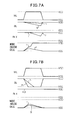
- FIG. 7A illustrates the case of the general SRAM illustrated in FIG. 1 and FIG. 7B illustrates the case of the basic SRAM.
- g and k illustrate the case where the characteristics of the transistor of the memory cell are normal and h and l illustrate the case where the characteristics of the transistor of the memory cell are poor.
- m and q illustrate the case where the characteristics of the transistor of the memory cell are normal and n and r illustrate the case where the characteristics of the transistor of the memory cell are poor.
- the capacitance of the bit line BL is large, in other words, a number of memory cells are connected to BL, and therefore, the voltage of the bit line BL drops only gradually. Therefore, when data is read from the memory cell the characteristic of which are poor, the voltage of the bit line BL does not drop sufficiently and in the state near VDD.
- the advanced processes applied to the manufacturing of the SRAM, etc. have large random variations, and therefore, depending on a certain balance of the six transistors within the memory cell, there is a case where the value of the cell is inverted and erroneous read results.
- the voltage of the bit line BL drops down to VSS before the value of the memory cell is inverted, and therefore, erroneous read is prevented.
- the reason is that the number of memory cells connected to the bit line BL is small and the wire length is short, and therefore, the capacitance is small. Because the bit line BL drops down to VSS before inversion, data L is written back to the memory cell as a result, and therefore, the poor stability is suppressed and reliability is improved.
- the global bit line does not consume power during the period of both the discharge phase (Dis-Charge phase) and the precharge phase (Pre-Charge phase).
- the amount of amplitude of the global bit line is determined by the capacitance ratio between the local bit line and the global bit line, and therefore, when the local bit line is shortened, the global bit line also needs to be shortened. The reason is that it is preferable to secure the minimum potential difference between the bit lines so as to operate the sense amplifier.
- the global bit line is shortened, it is preferable to provide a large number of circuits, such as the sense amplifier and the write circuit (write driver), and therefore, the macro size is increased and the reduction effect of power consumption is lessened as a result. Further, it is difficult to design a large capacity SRAM.
- An SRAM of a first embodiment has a general configuration similar to that of the basic SRAM illustrated in FIG. 3 .
- FIG. 8 is a diagram illustrating a configuration of a memory cell matrix of the SRAM of the first embodiment.
- FIG. 8 illustrates four columns of the circuit corresponding to one column illustrated in FIG. 4 . In actuality, a number of such columns are provided.
- Each column has pairs of global bit lines GBL ⁇ 0 >/GBLX ⁇ 0 > to GBL ⁇ 3 >/GBLX ⁇ 3 > and pairs of extended bit lines RD ⁇ 0 >/RDX ⁇ 0 > to RD ⁇ 3 >/RDX ⁇ 3 >.
- the pair of global bit lines and the pair of extended bit lines corresponding to each other are connected via extended connection transistors, respectively.
- a global connection circuit GC including global connection transistors is provided. While the global connection transistor is illustrated schematically so as to be provided within the sub block in FIG. 4 , here, it is illustrated schematically so as to be provided outside the sub block, however, there is no substantial difference.
- one global write circuit GWC is connected and in other columns, one global write circuit GWC is connected similarly.
- one global sense amplifier GSA is connected and in other columns, one global sense amplifier GSA is connected similarly.
- the sub block Bk 3 has a pair of local bit lines LBL ⁇ 3 > and LBLX ⁇ 3 > provided in parallel, a plurality (m+1) of memory cells C 0 to Cm connected between the pair of local bit lines, a local precharge circuit connected between the pair of local bit lines, a bit line (BL) capacitance shared circuit BC, and a write circuit (write driver) WC.
- a keeper circuit it may also be possible to provide a keeper circuit.
- Other sub blocks also have the same configuration.
- the BL capacitance shared circuit BC has two N-channel transistors and the drains of the two N-channel transistors are connected to the local bit line LBL ⁇ 3 > or LBLX ⁇ 3 > and the sources thereof are connected to a common connection line CLN.
- the common connection line CLN is connected in a shared manner to the source of the N-channel transistor of the BL capacitance shared circuit BC of the sub block corresponding to the four columns.
- the common connection line CLN may be connected to the source of the N-channel transistor of the BL capacitance shared circuit BC of the columns in the number other than four.
- FIG. 9 is a diagram illustrating in detail one memory cell C 0 , the precharge circuit, the BL capacitance shared circuit BC, the write driver WC, and the global connection circuit GC as to a column ⁇ 0 > and a column ⁇ 3 > on both sides illustrated in FIG. 8 .
- the memory cell C 0 has the same circuit configuration as that of the memory cell illustrated in FIG. 1 and is a normal static memory cell formed by six MOS transistors.
- the precharge circuit and the write driver WC have configurations somewhat different from those in the example illustrated in FIG. 4 , however, have similar functions and are widely-known circuits, and therefore, explanation is omitted.
- the global connection circuit GC has a transfer gate connected between the pair of local bit lines and the pair of global bit lines.
- the transfer gate is controlled by a connection signal.
- the transfer gate is provided and the connection state is controlled by a connection signal GC ⁇ 3 >.
- the transfer gate of the global connection circuit GC of other columns is the same and the connection signal of each column is independent and it is possible to control the transfer gate of each column independently of another.
- the transfer gate having the N-channel transistor and the P-channel transistor is used, however, it is also possible to use only the N-channel transistor or the P-channel transistor in place of the transfer gate.
- the BL capacitance shared circuit BC has the same configuration as that of the sense amplifier illustrated in FIG. 1 and FIG. 4 and the sources of the two N-channel transistors are connected to the common connection line CLN and the operating state is controlled by a local sense amplifier start signal LSAE.
- the SRAM of the first embodiment resembles the basic SRAM in the fundamental configuration.
- the SRAM of the first embodiment differs from the basic SRAM in that the common connection line CLN is provided and the source of the N-channel transistor of the sense amplifier SA provided within the BL capacitance shared circuit BC of each sub block is connected to the common connection line CLN.
- FIG. 10 is a time chart illustrating the operation of the SRAM of the first embodiment.
- a case is explained as an example, where the column ⁇ 3 > on the left side in FIG. 9 is selected and the write operation and the read operation are performed. The operation is performed in synchronization with the clock CLK.
- LSAE, GC ⁇ 3 >, COL ⁇ 3 >, GSAE ⁇ 3 >, and GWE ⁇ 3 > are at L (Low). LWE and GWE are maintained at L during the read operation regardless of the column. GC, COL, and GSAE of other columns are maintained at L during the read operation. Due to this, the pair of local bit lines LBL ⁇ 3 >/LBLX ⁇ 3 >, the pair of global bit lines GBL ⁇ 3 > GBLX ⁇ 3 >, and the pair of extended global bit lines RD ⁇ 3 >/RDX ⁇ 3 > are in the state of having been charged to VDD (H : High), respectively. GBL ⁇ 3 >/GBLX ⁇ 3 > are in the state of being connected to RD ⁇ 3 >/RDX ⁇ 3 >.
- the local precharge signal LPRE changes to VDD and the row selection signal WL changes to H and the write data WD/WDX is set.
- LPRE turns to L PC turns off and LBL ⁇ 3 > and LBLX ⁇ 3 > enter the separated state.
- any WL within the sub block turns to H the state of the memory cell where WL of each column has turned to H is read by the pair of local bit lines and the potential of the pair of local bit lines of each column changes, and further, LSAE changes to H and enlarges the potential difference at that time and turns one to H and the other to VSS (L : Low).
- one of the N-channel transistors of the sense amplifier SA turns on and a state is brought about where the local bit line the potential of which has dropped is connected to the common connection line CLN.
- This state is not limited to the selected column and the same in other columns.
- FIG. 9 illustrates a state where LBL ⁇ 3 > has turned to H and LBLX ⁇ 3 > to L, and LBLX ⁇ 3 > is connected to CLN, LBL ⁇ 0 > has turned to L and LBLX ⁇ 0 > to H, and LBLX ⁇ 0 > is connected to CLN and the connected local bit line is indicated by a broken line.
- FIG. 9 illustrates a state where LBL ⁇ 3 > has turned to H and LBLX ⁇ 3 > to L, and LBLX ⁇ 3 > is connected to CLN, LBL ⁇ 0 > has turned to L and LBLX ⁇ 0 > to H, and LBLX ⁇ 0 > is connected to CLN and the connected local bit line is indicated by a broken line.
- LBL ⁇ 3 > has turned to H and LBLX ⁇ 3 > to L
- LBL ⁇ 0 > to LBL ⁇ 2 > have turned to L
- LBLX ⁇ 0 > to LBLX ⁇ 2 > have turned to H. Consequently, a state is brought about where the four local bit lines at L are connected, and therefore, a state is brought about where the capacitance of the local bit lines at L increases four times.
- LBLX ⁇ 3 > has a capacitance of the local bit line the length of which is four times because LBL ⁇ 0 > to LBL ⁇ 2 > of the other three columns are connected.
- LSAE and WL change to L. Even when LSAE changes to L, the state is maintained where LBL ⁇ 0 > to LBL ⁇ 2 > are connected to LBLX ⁇ 3 >.
- LBLX ⁇ 3 > when LBLX ⁇ 3 > is at L, the potential of LBLX ⁇ 3 > and RDX ⁇ 3 > drops and the potential of GBL ⁇ 3 > and RD ⁇ 3 > is maintained at H.
- LBLX ⁇ 3 > is connected to LBLX ⁇ 0 > to LBLX ⁇ 2 > and the capacitance increases four times, and therefore, it is possible to increase the amount of drop of the potential of GBLX ⁇ 3 > and RDX ⁇ 3 >. Further, if the amount of drop of potential is the same, it is possible to increase the length of the pair of local bit lines. Even if LBL ⁇ 3 > and GBL ⁇ 3 >, and LBL ⁇ 3 > and RD ⁇ 3 > are connected, the potential of both is VDD, and therefore, the potential hardly changes.
- LBL ⁇ 0 >/LBLX ⁇ 0 > to LBL ⁇ 2 >/LBLX ⁇ 2 > of the columns other than the selected column enter the state where the potential of the side that is at L has somewhat risen by the charge share, however, WL is at L, and therefore, the state of the memory cell is not affected.
- LBL ⁇ 0 >/LBLX ⁇ 0 > to LBL ⁇ 3 >/LBLX ⁇ 3 >, GBL ⁇ 0 >/GBLX ⁇ 0 > to GBL ⁇ 3 >/GBLX ⁇ 3 >, and RD ⁇ 0 >/RDX ⁇ 3 > are charged to VDD, respectively.
- LSAE, LWE, GC ⁇ 3 >, COL ⁇ 3 >, GSAE ⁇ 3 >, and GWE ⁇ 3 > are at L (Low).
- GSAE is maintained at L during the write operation regardless of the column.
- GC, COL, GSAE and GWE of other columns are maintained at L during the write operation. Due to this, the pair of local bit lines LBL ⁇ 3 >/LBLX ⁇ 3 >, the pair of global bit lines GBL ⁇ 3 > GBLX ⁇ 3 >, and the pair of extended global bit lines RD ⁇ 3 >/RDX ⁇ 3 > are in the state of having been charged to VDD, respectively.
- GBL ⁇ 3 >/GBLX ⁇ 3 > are in the state of being connected to RD ⁇ 3 >/RDX ⁇ 3 >.
- the local precharge signal LPRE changes to H (High) and the row selection signal WL changes to H and the write data WD/WDX is set.
- LPRE turns to H
- PC turns off and LBL ⁇ 3 > and LBLX ⁇ 3 > enter the separated state.
- the state of the memory cell where WL of each column has turned to H is read, the potential of the pair of local bit lines of each column changes, and further, LSAE changes to H and enlarges the potential difference at that time and turns one to VDD and the other to VSS.
- LBLX ⁇ 3 > enters the state of being connected to LBLX ⁇ 0 > to LBLX ⁇ 2 > as at the time of read.
- LSAE changes to L.
- COL ⁇ 3 > and GWE ⁇ 3 > of the selected column of target of write change to H and GBL ⁇ 3 >/GBLX ⁇ 3 > change to the state in correspondence to the data WD/WDX.
- LBLX ⁇ 0 > to LBLX ⁇ 2 > connected to LBLX ⁇ 3 > is cut off from CLN when the N-channel transistor of SA turns off as the potential of LBLX ⁇ 3 > (common connection line CLN) rises.
- LBL ⁇ 3 >/LBLX ⁇ 3 > it may also be possible to maintain GC ⁇ 3 > at L.
- the memory cell in which WL of the selected column has turned to H changes to the state in correspondence to LBL ⁇ 3 >/LBLX ⁇ 3 > and it is possible to write the data WD/WDX to the memory cell of target of write.
- LBL ⁇ 0 >/LBLX ⁇ 0 > to LBL ⁇ 2 >/LBLX ⁇ 2 > in the columns other than the selected column enter the state in correspondence to the stored data of the memory cell in which WL has turned to H and are cut off from GBL ⁇ 0 >/GBLX ⁇ 0 > to GBL ⁇ 2 >/GBLX ⁇ 2 >, and therefore, maintain the state.
- the memory cell in which WL is at H stores the state at that time. Due to this, the memory cell of the selected column enters the state in correspondence to the data WD/WDX and the memory cells in other columns maintain the stored state.
- the BL capacitance shared circuit BC is implemented by a sense amplifier, however, it may also be implemented by another circuit.
- an SRAM of an embodiment in which the BL capacitance shared circuit BC is implemented by another circuit is explained.
- An SRAM of a second embodiment has a general configuration similar to that of the SRAM of the first embodiment and only the configuration of the BL capacitance shared circuit BC is different.
- FIG. 11 is a diagram illustrating in detail the one memory cell C 0 , the precharge circuit, the BL capacitance shared circuit BC, the write driver WC, and the global connection circuit GC within the sub block as to the column ⁇ 0 > and the column ⁇ 3 > of the SRAM of the second embodiment.
- the BL capacitance shared circuit BC has the sense amplifier SA and a shared connection circuit BCA.
- the sense amplifier SA is the sense amplifier illustrated in FIG. 1 and differs from that of the first embodiment in not being connected to the common connection line CLN and others are the same, and therefore, explanation is omitted.
- the shared connection circuit BCA has two N-channel transistors and two columns of two P-channel transistors and a transfer gate connected in series between the power source VDD and GND.
- the two N-channel transistors are connected between the pair of local bit lines and the common connection line CLN and the gate is connected to the connection node of the P-channel transistor and the transfer gate.
- the gate of the P-channel transistor in the first stage is connected to the pair of local bit line, respectively.
- the P-channel transistor in the second stage and one of the gate inputs of the transfer gate are connected to the output control signal terminal of the write driver WC on the opposite output side.
- a signal which is the inverted local precharge signal LPRE, is applied to the other gate of the transfer gate.
- the two N-channel transistors turn on when LPRE is at H, LWE is at L or WC writes data different from the previous data, and the local bit line turns to L.
- the SRAM of the second embodiment operates in accordance with the time chart illustrated in FIG. 10 .
- a case where LSAE is changed to H is explained.
- LPRE and WL are at H and LWE is at L.
- LSAE is changed to H
- one of the pair of local bit lines changes to L and in the shared connection circuit BCA
- the transistor of the two N-channel transistors which is connected to the local bit line at L, turns on. Due to this, the state is brought about where the four local bit lines are connected.
- the BL capacitance shared circuit BC has the sense amplifier SA and the shared connection circuit BCA, however, without the provision of the sense amplifier SA, the same operation is performed.
- the operation is the same as that of the basic SRAM explained in FIG. 4 .
- the difference from the basic SRAM lies in that one of the two N-channel transistors of the shared connection circuit BCA turns on in accordance with the potential of the local bit line and the state is brought about where the four local bit lines are connected.
- FIG. 12 is a diagram illustrating in detail the one memory cell C 0 , the precharge circuit, the BL capacitance shared circuit BC, the write driver WC, and the global connection circuit GC within the sub block as to the column ⁇ 0 > and the column ⁇ 3 > of an SRAM of a third embodiment.
- the BL capacitance shared circuit BC has the sense amplifier SA and the shared connection circuit BCA.
- the sense amplifier SA is the sense amplifier illustrated in FIG. 1 and differs from that of the first embodiment in not being connected to the common connection line CLN and others are the same, and therefore, explanation is omitted.
- the shared connection circuit BCA has two N-channel transistors and two columns of one P-channel transistor and N-channel transistor connected in series between the power source VDD and GND.
- the two N-channel transistors are connected between the pair of local bit lines and the common connection line CLN and the gate is connected to the connection node of the P-channel transistor and the N-channel transistor in the corresponding column.
- the gate of the P-channel transistor in the first stage is connected to the pair of local bit line, respectively.
- a signal which is the inverted local precharge signal LPRE, is applied.
- the two N-channel transistors turn on when LPRE is at H and the local bit line turns to L.
- FIG. 13 is the time chart illustrating the operation of the SRAM of the third embodiment.
- the operation at the time of read operation is the same as that of the time chart in FIG. 10 , and therefore, explanation is omitted.
- WL, LSAE, GC ⁇ 3 >, and GSA ⁇ 3 > are at L (Low).
- GSAE is maintained at L during the write operation regardless of the column.
- GC, COL, GSAE, and GWE in other columns are maintained at L during the write operation. Due to this, the pair of global bit lines GBL ⁇ 3 >/GBLX ⁇ 3 > and the pair of extended global bit lines RD ⁇ 3 >/RDX ⁇ 3 > are in the states of having been charged to H, respectively.
- GBL ⁇ 3 >/GBLX ⁇ 3 > are in the state of being connected to RD ⁇ 3 >/RDX ⁇ 3 >.
- the pair of local bit lines LBL ⁇ 3 >/LBLX ⁇ 3 > maintains the previous state where one is at H and the other is at L.
- LPRE, LSAE, LWE, GC ⁇ 3 >, COL ⁇ 3 >, and GWE ⁇ 3 > change to L and LBL ⁇ 0 >/LBLX ⁇ 0 > to LBL ⁇ 3 >/LBLX ⁇ 3 >, GBL ⁇ 0 >/GBLX ⁇ 0 > to GBL ⁇ 3 >/GBLX ⁇ 3 >, and RD ⁇ 0 >/RDX ⁇ 3 > are charged to VDD, respectively.
- FIG. 14 is a diagram illustrating a configuration of a memory cell matrix of an SRAM of a fourth embodiment.
- the SRAM of the fourth embodiment differs from that of the first embodiment in that the write driver WC is removed from the sub blocks B 00 to Bk 0 . . . B 03 to Bk 3 and in that the global connection circuit GC has the N-channel transistor in place of the transfer gate.
- FIG. 15 is a diagram illustrating in details the one memory cell C 0 , the precharge circuit, the BL capacitance shared circuit BC, and the global connection circuit GC within the sub block as to the column ⁇ 0 > and the column ⁇ 3 > on both sides illustrated in FIG. 14 .
- the BL capacitance shared circuit BC includes the sense amplifier as in the first embodiment and is connected to the sense amplifier of another column via the common connection line CLN.
- the SRAM of the fourth embodiment operates in accordance with the time chart in FIG. 10 .
- FIG. 16 is a diagram illustrating in details the one memory cell C 0 , the precharge circuit, the BL capacitance shared circuit BC, and the global connection circuit GC within the sub block as to the column ⁇ 0 > and the column ⁇ 3 > in an SRAM of a fifth embodiment.
- the SRAM of the fifth embodiment differs from that of the third embodiment in that the write driver WC is removed from the sub blocks BOO to Bk 0 . . . B 03 to Bk 3 .
- the SRAM of the fifth embodiment operates in accordance with the time chart in FIG. 13 .
- FIG. 17 is a diagram illustrating a configuration of a memory cell matrix of an SRAM of a sixth embodiment.
- the SRAM of the sixth embodiment differs from that of the first embodiment in that the four pairs of global bit lines GBL ⁇ 0 >/GBLX ⁇ 0 > to GBL ⁇ 3 >/GBLX ⁇ 3 > of the four columns are integrated into one pair of global bit lines GBL/GBLX at the end part.
- the pairs of extended global bit lines RD ⁇ 0 >/RDX ⁇ 0 > to RD ⁇ 3 >/RDX ⁇ 3 > are integrated into one pair of extended global bit lines RD/RDX.
- LWE that activates the write driver WC of each column is separated into LWE ⁇ 0 > to LWE ⁇ 3 >, and therefore, it is possible to control the operating state of each write driver WC independently. Further, the SRAM of the sixth embodiment controls the operating state of the global write circuit GWC to which the global precharge GPRE is integrated in place of COL ⁇ 0 > to COL ⁇ 3 >.
- FIG. 18 is a diagram illustrating in details the one memory cell C 0 , the precharge circuit, the BL capacitance shared circuit BC, the write driver WC, and the global connection circuit GC within the sub block as to the column ⁇ 0 > and the column ⁇ 3 > on both sides illustrated in FIG. 17 .
- FIG. 19 is a time chart illustrating the operation of the SRAM of the sixth embodiment. As illustrated in FIG. 19 , in the sixth embodiment, at the time of write operation, LWE ⁇ 3 > and GPRE change to H and return to L at the same timing as that of GC ⁇ 3 > and GWE. Explanation of the operation is the same as that of the first embodiment, and therefore, omitted.
- An SRAM of a seventh embodiment has a configuration similar to that of the SRAM of the sixth embodiment illustrated in FIG. 17 and the BL capacitance shared circuit BC has the same configuration as that of the BL capacitance shared circuit BC of the second embodiment.
- FIG. 20 is a diagram illustrating in details the one memory cell C 0 , the precharge circuit, the BL capacitance shared circuit BC, the write driver WC, and the global connection circuit GC within the sub block as to the column ⁇ 0 > and the column ⁇ 3 > in the SRAM of the seventh embodiment.
- the SRAM of the seventh embodiment has a general configuration similar to that of the SRAM of the sixth embodiment and the BL capacitance shared circuit BC is similar to that explained in the second embodiment, and therefore, explanation is omitted.
- the SRAM of the seventh embodiment operates in accordance with the time chart in FIG. 19 .
- An SRAM of an eighth embodiment has a configuration similar to that of the SRAM of the sixth embodiment and the BL capacitance shared circuit BC has the same configuration as that of the BL capacitance shared circuit BC of the third embodiment.
- FIG. 21 is a diagram illustrating in details the one memory cell C 0 , the precharge circuit, the BL capacitance shared circuit BC, the write driver WC, and the global connection circuit GC within the sub block as to the column ⁇ 0 > and the column ⁇ 3 > in the SRAM of the eighth embodiment.
- FIG. 22 is a time chart illustrating the operation of the SRAM of the eighth embodiment. As illustrated in FIG. 22 , in the eighth embodiment, at the time of write operation, LWE ⁇ 3 > and GPRE change to H and return to L at the same timing as that of GC ⁇ 3 > and GWE. Explanation of the operation is the same as that of the third embodiment, and therefore, is omitted.
- FIG. 23 is a diagram illustrating a configuration of a memory cell matrix of an SRAM of a ninth embodiment.
- the SRAM of the ninth embodiment differs from that of the fourth embodiment in that the four pairs of global bit lines GBL ⁇ 0 >/GBLX ⁇ 0 > to GBL ⁇ 3 >/GBLX ⁇ 3 > of the four columns are integrated into one pair of global bit lines GBL/GBLX at the end part.
- the integration of the pair of global bit lines, the pair of extended global bit lines, the global write circuit, and the global sense amplifier is performed as in the sixth embodiment.
- FIG. 24 is a diagram illustrating in details the one memory cell C 0 , the precharge circuit, the BL capacitance shared circuit BC, and the global connection circuit GC within the sub block as to the column ⁇ 0 > and the column ⁇ 3 > on both sides illustrated in FIG. 23 .
- the SRAM of the ninth embodiment has a general configuration similar to that of the SRAM of the fourth embodiment and the integration of the pairs of global bit lines, etc., is similar to that in the sixth embodiment, and therefore, explanation is omitted.
- the SRAM of the ninth embodiment operates in accordance with the time chart in FIG. 10 .
- FIG. 25 is a diagram illustrating in details the one memory cell C 0 , the precharge circuit, the BL capacitance shared circuit BC, and the global connection circuit GC within the sub block as to the column ⁇ 0 > and the column ⁇ 3 > on both sides in an SRAM of a tenth embodiment.
- the SRAM of the tenth embodiment has a general configuration similar to that of the SRAM of the fifth embodiment and the integration of the pairs of global bit lines, etc., is similar to that in the sixth embodiment, and therefore, explanation is omitted.
- the SRAM of the tenth embodiment operates in accordance with the time chart in FIG. 13 .
- an SRAM the power consumption of which has been reduced while maintaining the operating speed and reliability is realized.
Landscapes
- Engineering & Computer Science (AREA)
- Microelectronics & Electronic Packaging (AREA)
- Computer Hardware Design (AREA)
- Static Random-Access Memory (AREA)
Abstract
Description
- [Patent Document 1] Japanese Laid Open Patent Document No. 2003-151280
- [Patent Document 2] Japanese Laid Open Patent Document No. E01-241093
Claims (5)
Applications Claiming Priority (2)
| Application Number | Priority Date | Filing Date | Title |
|---|---|---|---|
| JP2011173764A JP5760829B2 (en) | 2011-08-09 | 2011-08-09 | Static RAM |
| JP2011-173764 | 2011-08-09 |
Publications (2)
| Publication Number | Publication Date |
|---|---|
| US20130039120A1 US20130039120A1 (en) | 2013-02-14 |
| US8824197B2 true US8824197B2 (en) | 2014-09-02 |
Family
ID=47677457
Family Applications (1)
| Application Number | Title | Priority Date | Filing Date |
|---|---|---|---|
| US13/561,420 Expired - Fee Related US8824197B2 (en) | 2011-08-09 | 2012-07-30 | Static RAM |
Country Status (3)
| Country | Link |
|---|---|
| US (1) | US8824197B2 (en) |
| JP (1) | JP5760829B2 (en) |
| CN (1) | CN102956262B (en) |
Cited By (3)
| Publication number | Priority date | Publication date | Assignee | Title |
|---|---|---|---|---|
| US20160064044A1 (en) * | 2013-04-08 | 2016-03-03 | Surecore Limited | Memory with local-/global bit line architecture and additional capacitance for global bit line discharge in reading |
| US9412439B1 (en) * | 2015-01-16 | 2016-08-09 | Taiwan Semiconductor Manufacturing Company, Ltd. | Hybrid TFET-MOSFET circuit design |
| US11568924B2 (en) | 2020-10-27 | 2023-01-31 | Samsung Electronics Co., Ltd. | Static random access memory (SRAM) devices and methods of operating the same |
Families Citing this family (12)
| Publication number | Priority date | Publication date | Assignee | Title |
|---|---|---|---|---|
| JP5776418B2 (en) * | 2011-07-29 | 2015-09-09 | 富士通セミコンダクター株式会社 | Semiconductor memory device and method for controlling semiconductor memory device |
| CN104217752A (en) * | 2013-06-03 | 2014-12-17 | 辉达公司 | Multi-port memory system, and write circuit and read circuit for multi-port memory |
| JP6424448B2 (en) * | 2014-03-28 | 2018-11-21 | 株式会社ソシオネクスト | Semiconductor memory device |
| US9431098B1 (en) * | 2015-08-10 | 2016-08-30 | International Business Machines Corporation | Structure for reducing pre-charge voltage for static random-access memory arrays |
| CN105895148B (en) * | 2016-05-20 | 2018-11-09 | 西安紫光国芯半导体有限公司 | A kind of Static RAM of low-power consumption and its control method of write operation |
| JP2020042873A (en) * | 2018-09-11 | 2020-03-19 | 株式会社東芝 | Semiconductor storage device |
| JP7351307B2 (en) | 2018-09-25 | 2023-09-27 | 株式会社ソシオネクスト | Semiconductor device and its manufacturing method |
| US11532351B2 (en) * | 2020-05-08 | 2022-12-20 | Taiwan Semiconductor Manufacturing Company, Ltd. | Memory device with additional write bit lines |
| CN115602207A (en) * | 2021-07-07 | 2023-01-13 | 长鑫存储技术有限公司(Cn) | Data storage circuit, its control method, and storage device |
| US12237038B2 (en) | 2022-02-25 | 2025-02-25 | Changxin Memory Technologies, Inc. | Local sensing amplifier and memory |
| US20240420748A1 (en) * | 2023-06-16 | 2024-12-19 | Nvidia Corp. | Shared metal wire capacitance for negative bit-line |
| GB2634266A (en) * | 2023-10-04 | 2025-04-09 | Ibm | Memory device, assist cell and double assist cell for a memory device |
Citations (3)
| Publication number | Priority date | Publication date | Assignee | Title |
|---|---|---|---|---|
| JPH01241093A (en) | 1988-03-22 | 1989-09-26 | Fujitsu Ltd | Semiconductor memory |
| US20030090951A1 (en) | 2001-11-09 | 2003-05-15 | Fujitsu Limited | Semiconductor memory |
| US20090154265A1 (en) * | 2005-11-22 | 2009-06-18 | Samsung Electronics Co., Ltd. | Semiconductor memory device with hierarchical bit line structure |
Family Cites Families (5)
| Publication number | Priority date | Publication date | Assignee | Title |
|---|---|---|---|---|
| JP2004103081A (en) * | 2002-09-06 | 2004-04-02 | Renesas Technology Corp | Semiconductor storage device |
| KR100772721B1 (en) * | 2005-09-29 | 2007-11-02 | 주식회사 하이닉스반도체 | Semiconductor memory device |
| US8223567B2 (en) * | 2007-12-15 | 2012-07-17 | Qualcomm Incorporated | Memory read stability using selective precharge |
| JP2010170641A (en) * | 2009-01-26 | 2010-08-05 | Fujitsu Ltd | Semiconductor memory circuit device and read control method |
| JP5505274B2 (en) * | 2010-11-22 | 2014-05-28 | 富士通セミコンダクター株式会社 | Static RAM |
-
2011
- 2011-08-09 JP JP2011173764A patent/JP5760829B2/en not_active Expired - Fee Related
-
2012
- 2012-07-30 US US13/561,420 patent/US8824197B2/en not_active Expired - Fee Related
- 2012-08-09 CN CN201210286777.XA patent/CN102956262B/en not_active Expired - Fee Related
Patent Citations (4)
| Publication number | Priority date | Publication date | Assignee | Title |
|---|---|---|---|---|
| JPH01241093A (en) | 1988-03-22 | 1989-09-26 | Fujitsu Ltd | Semiconductor memory |
| US20030090951A1 (en) | 2001-11-09 | 2003-05-15 | Fujitsu Limited | Semiconductor memory |
| JP2003151280A (en) | 2001-11-09 | 2003-05-23 | Fujitsu Ltd | Semiconductor storage device |
| US20090154265A1 (en) * | 2005-11-22 | 2009-06-18 | Samsung Electronics Co., Ltd. | Semiconductor memory device with hierarchical bit line structure |
Cited By (4)
| Publication number | Priority date | Publication date | Assignee | Title |
|---|---|---|---|---|
| US20160064044A1 (en) * | 2013-04-08 | 2016-03-03 | Surecore Limited | Memory with local-/global bit line architecture and additional capacitance for global bit line discharge in reading |
| US9406351B2 (en) * | 2013-04-08 | 2016-08-02 | Surecore Limited | Memory with local-/global bit line architecture and additional capacitance for global bit line discharge in reading |
| US9412439B1 (en) * | 2015-01-16 | 2016-08-09 | Taiwan Semiconductor Manufacturing Company, Ltd. | Hybrid TFET-MOSFET circuit design |
| US11568924B2 (en) | 2020-10-27 | 2023-01-31 | Samsung Electronics Co., Ltd. | Static random access memory (SRAM) devices and methods of operating the same |
Also Published As
| Publication number | Publication date |
|---|---|
| CN102956262B (en) | 2015-12-09 |
| US20130039120A1 (en) | 2013-02-14 |
| JP5760829B2 (en) | 2015-08-12 |
| JP2013037743A (en) | 2013-02-21 |
| CN102956262A (en) | 2013-03-06 |
Similar Documents
| Publication | Publication Date | Title |
|---|---|---|
| US8824197B2 (en) | Static RAM | |
| US8797786B2 (en) | Static RAM | |
| TWI514416B (en) | A memory cell and a dynamic memory array | |
| US8116149B2 (en) | Circuit and method for small swing memory signals | |
| US7656732B2 (en) | Semiconductor storage device | |
| CN1759448B (en) | Sense amplifier, memory device including same, computer system and method | |
| US20070081407A1 (en) | Semiconductor memory | |
| US9305635B2 (en) | High density memory structure | |
| JP6308218B2 (en) | Semiconductor memory device | |
| US9019782B2 (en) | Dual rail memory architecture | |
| US20080205178A1 (en) | DRAM writing ahead of sensing scheme | |
| US8279692B2 (en) | Semiconductor device having hierarchical data line structure and control method thereof | |
| US6570799B1 (en) | Precharge and reference voltage technique for dynamic random access memories | |
| JP2010218671A (en) | Semiconductor memory device | |
| CN100573712C (en) | Memory output stage circuit and method for outputting memory data | |
| JP5867275B2 (en) | Semiconductor memory device and data writing method thereof | |
| US12237000B2 (en) | Sense amplifier circuit with precharge, memory device including the same and sensing method of memory device | |
| JP2007109325A (en) | Semiconductor memory device | |
| TWI697008B (en) | Bitline write driver | |
| TW202119416A (en) | Memory write operation apparatus and method | |
| US7352648B2 (en) | Semiconductor memory | |
| US20250078915A1 (en) | Low power read circuit for multi-bank memory | |
| TWM593052U (en) | Write driver circuit | |
| JP2004272944A (en) | Semiconductor storage device | |
| CN104851449A (en) | Pseudo-differential read scheme for dual port RAM |
Legal Events
| Date | Code | Title | Description |
|---|---|---|---|
| AS | Assignment |
Owner name: FUJITSU SEMICONDUCTOR LIMITED, JAPAN Free format text: ASSIGNMENT OF ASSIGNORS INTEREST;ASSIGNOR:MORIWAKI, SHINICHI;REEL/FRAME:028675/0798 Effective date: 20120719 |
|
| STCF | Information on status: patent grant |
Free format text: PATENTED CASE |
|
| AS | Assignment |
Owner name: SOCIONEXT INC., JAPAN Free format text: ASSIGNMENT OF ASSIGNORS INTEREST;ASSIGNOR:FUJITSU SEMICONDUCTOR LIMITED;REEL/FRAME:038197/0008 Effective date: 20160216 Owner name: FUJITSU SEMICONDUCTOR LIMITED, JAPAN Free format text: CHANGE OF ADDRESS;ASSIGNOR:FUJITSU SEMICONDUCTOR LIMITED;REEL/FRAME:038361/0492 Effective date: 20150714 |
|
| MAFP | Maintenance fee payment |
Free format text: PAYMENT OF MAINTENANCE FEE, 4TH YEAR, LARGE ENTITY (ORIGINAL EVENT CODE: M1551) Year of fee payment: 4 |
|
| FEPP | Fee payment procedure |
Free format text: MAINTENANCE FEE REMINDER MAILED (ORIGINAL EVENT CODE: REM.); ENTITY STATUS OF PATENT OWNER: LARGE ENTITY |
|
| LAPS | Lapse for failure to pay maintenance fees |
Free format text: PATENT EXPIRED FOR FAILURE TO PAY MAINTENANCE FEES (ORIGINAL EVENT CODE: EXP.); ENTITY STATUS OF PATENT OWNER: LARGE ENTITY |
|
| STCH | Information on status: patent discontinuation |
Free format text: PATENT EXPIRED DUE TO NONPAYMENT OF MAINTENANCE FEES UNDER 37 CFR 1.362 |
|
| FP | Lapsed due to failure to pay maintenance fee |
Effective date: 20220902 |