US8822979B2 - Arrangement comprising a support and super-conductive film, vortex diode comprising said type of arrangement and use of vortex diodes for filters - Google Patents
Arrangement comprising a support and super-conductive film, vortex diode comprising said type of arrangement and use of vortex diodes for filters Download PDFInfo
- Publication number
- US8822979B2 US8822979B2 US11/988,522 US98852206A US8822979B2 US 8822979 B2 US8822979 B2 US 8822979B2 US 98852206 A US98852206 A US 98852206A US 8822979 B2 US8822979 B2 US 8822979B2
- Authority
- US
- United States
- Prior art keywords
- perforation
- perforations
- vortex diode
- accordance
- vortex
- Prior art date
- Legal status (The legal status is an assumption and is not a legal conclusion. Google has not performed a legal analysis and makes no representation as to the accuracy of the status listed.)
- Expired - Fee Related, expires
Links
Images




Classifications
-
- H01L39/148—
-
- H—ELECTRICITY
- H10—SEMICONDUCTOR DEVICES; ELECTRIC SOLID-STATE DEVICES NOT OTHERWISE PROVIDED FOR
- H10N—ELECTRIC SOLID-STATE DEVICES NOT OTHERWISE PROVIDED FOR
- H10N60/00—Superconducting devices
- H10N60/20—Permanent superconducting devices
- H10N60/208—Permanent superconducting devices based on Abrikosov vortices
-
- H01L39/14—
-
- H01L39/2483—
-
- H—ELECTRICITY
- H10—SEMICONDUCTOR DEVICES; ELECTRIC SOLID-STATE DEVICES NOT OTHERWISE PROVIDED FOR
- H10N—ELECTRIC SOLID-STATE DEVICES NOT OTHERWISE PROVIDED FOR
- H10N60/00—Superconducting devices
- H10N60/01—Manufacture or treatment
- H10N60/0268—Manufacture or treatment of devices comprising copper oxide
- H10N60/0828—Introducing flux pinning centres
-
- H—ELECTRICITY
- H10—SEMICONDUCTOR DEVICES; ELECTRIC SOLID-STATE DEVICES NOT OTHERWISE PROVIDED FOR
- H10N—ELECTRIC SOLID-STATE DEVICES NOT OTHERWISE PROVIDED FOR
- H10N60/00—Superconducting devices
- H10N60/20—Permanent superconducting devices
-
- Y—GENERAL TAGGING OF NEW TECHNOLOGICAL DEVELOPMENTS; GENERAL TAGGING OF CROSS-SECTIONAL TECHNOLOGIES SPANNING OVER SEVERAL SECTIONS OF THE IPC; TECHNICAL SUBJECTS COVERED BY FORMER USPC CROSS-REFERENCE ART COLLECTIONS [XRACs] AND DIGESTS
- Y10—TECHNICAL SUBJECTS COVERED BY FORMER USPC
- Y10T—TECHNICAL SUBJECTS COVERED BY FORMER US CLASSIFICATION
- Y10T428/00—Stock material or miscellaneous articles
- Y10T428/24—Structurally defined web or sheet [e.g., overall dimension, etc.]
- Y10T428/24273—Structurally defined web or sheet [e.g., overall dimension, etc.] including aperture
- Y10T428/24298—Noncircular aperture [e.g., slit, diamond, rectangular, etc.]
-
- Y—GENERAL TAGGING OF NEW TECHNOLOGICAL DEVELOPMENTS; GENERAL TAGGING OF CROSS-SECTIONAL TECHNOLOGIES SPANNING OVER SEVERAL SECTIONS OF THE IPC; TECHNICAL SUBJECTS COVERED BY FORMER USPC CROSS-REFERENCE ART COLLECTIONS [XRACs] AND DIGESTS
- Y10—TECHNICAL SUBJECTS COVERED BY FORMER USPC
- Y10T—TECHNICAL SUBJECTS COVERED BY FORMER US CLASSIFICATION
- Y10T428/00—Stock material or miscellaneous articles
- Y10T428/24—Structurally defined web or sheet [e.g., overall dimension, etc.]
- Y10T428/24273—Structurally defined web or sheet [e.g., overall dimension, etc.] including aperture
- Y10T428/24322—Composite web or sheet
Definitions
- the invention relates to an arrangement made of substrate and superconducting film, a vortex diode including such an arrangement, and the use of vortex diodes for filters.
- Resonators for filtering signals such as e.g. cavity resonators, dielectric resonators, ⁇ /2 resonators, and LC resonators are known from the prior art. It is disadvantageous that the known resonators are relatively large. Miniaturization of these filters is subject to limits because such miniaturization normally leads to a decrease in quality.
- Filtering a plurality of frequency contributions is normally accomplished by splitting the signal into different channels.
- the signal in these channels is tested for the different frequencies using additional electronic devices.
- a complex method for scanning frequencies is known. In this case, as well, the need for downstream electronics and in some cases amplification of the output signal is disadvantageous.
- Type II superconductors for filter purposes are known from the prior art. They completely displace a magnetic field until the value of the magnetic flux of H c1 ⁇ H c , but remain superconducting up to a value of H c2 >H c , H c being the thermodynamically defined critical magnetic field strength.
- Type II superconductors In contrast to Type I superconductors, in Type II superconductors the magnetic field partially penetrates into the superconductor for fields at values between H c1 and H c2 . Due to the quantum condition that applies for the magnetic flux and due to the energetically advantageous formation of normal superconducting limiting surfaces, the magnetic field can be present solely as vortices.
- ⁇ o 2 ⁇ 10 ⁇ 15 Weber
- the magnetic flux equals whole-number multiples of the flux quantum.
- Type II superconductors In order to use Type II superconductors as conductor materials, e.g. for magnetic coils or cables, they must be able to carry relatively large currents in the magnetic field with no losses. For this, the vortices are fixed locally via pinning centers. If they were not fixed, they would move through the superconductor when a current was applied due to the Lorentz force F L and would generate dissipative effects and thus an electrical resistance. Type II superconductors with such pinning centers are also called hard superconductors.
- the electronic device includes e.g. an HF converter adapted to the application or an HF power measuring device.
- the object of the invention is to provide an arrangement made of a substrate and a superconducting film for a filter having direct conversion of the signal to a DC signal. It is a further object of the invention to provide a filter with which a plurality of frequency contributions can be simultaneously filtered out, without an electronic device downstream, and can be converted to a DC signal.
- the object is attained by an arrangement with all of the features in accordance with claim 1 and by a vortex diode and by using vortex diodes for a filter in accordance with subordinate claims.
- the inventive arrangement includes a substrate and a superconducting film arranged thereon, preferably from a Type II superconductor.
- the superconducting film has a plurality of perforations for embodying a perforation grid in the film.
- the arrangement is characterized by rows of round perforations that grow progressively larger or triangular perforations that are arranged in a selected orientation in the superconducting film. Both geometries in the superconducting film have proved advantageous in attaining the object.
- round and triangular also encompass substantially round or triangular structures.
- round can include all round structures, that is, oval or even e.g. ellipsoidal structures, in addition to the preferred circular structures.
- Cited simply as examples are triangles in a wandering pattern in the superconducting film or even in combination with round perforations. However, other suitable combinations of these features can also produce the desired signal conversion effect.
- the perforation grid in the superconducting film has perforations having a size between preferably 50 and 50,000 nanometers.
- the interval between perforations, from perforation center to perforation center, should preferably range from about 100 to 50,000 nanometers.
- BaSrCaCuO compounds, Tl-HTSL, Nb, Pb, Nb compounds, and A15 superconductors are also conceivable as materials. These materials can advantageously be deposited as a thin film on high frequency-capable substrates and are so-called Type II superconductors having great penetration depth and thus small critical fields B c1 .
- the superconducting film can be arranged on the substrate as a thin film, in particular with a thickness of 0.1 to 2.0 ⁇ m.
- substrate materials are in particular high frequency-capable materials, e.g. single crystals made of sapphire, LaAlO 3 , MgO, or silicon.
- the inventive arrangement made of superconducting film and substrate is embodied such that it can embody a vortex diode.
- the asymmetry from the shape can be embodied by non-equilateral triangles arranged in rows or by size, e.g. by progressive perforation sizes, or by the arrangement of the perforations themselves, e.g. in a wavy or wandering arrangement.
- the guided motion of the vortices can be determined and the DC signal can be produced.
- the guided motion of the vortices is prespecified in a direction to the end of the superconducting film or the stripline.
- the vortices are moved from one perforation to the next in a direction prespecified by the asymmetry in the perforation grid of the superconducting film.
- an alternating current signal produces the direct voltage signal using the preferred direction of the guided motion of the vortices.
- the guided motion of the vortices can be caused by a regular grid of triangular perforations that are not equilateral but that are isosceles.
- Perforations made of acute-angled triangles with the tips oriented perpendicular to the current direction cause a preferential guided vortex motion in the direction of the acute angle.
- the physical cause of the preferential guided vortex motion is the locally different density of the screening current that flows around each perforation in the superconductor and screens the magnetic flux to the superconductor in the perforation.
- the current density is exceeded at the tip of the triangle, and therefore nucleation of vortices is more probable at this location, due to the locally reduced superconducting properties, than at other locations of the edge of the perforation. Therefore the guided motion of the vortices out of the tip of the triangle is also simpler because their nucleation is easier.
- the direction of the Lorentz force can also be utilized on the vortices perpendicular to current and magnetic field.
- the arrangement of the perforations suitably.
- a wavy, wandering arrangement of rows of identical perforations can be used that on the one hand connect both sides of the stripline and on the other hand in which the vortices run in nearly parallel to the current at the reversal points (so-called force-free configuration, since the Lorentz force is perpendicular to the current) in order then after the current has been inverted to run out perpendicular to the current (maximum Lorentz force) into the next arc.
- the wandering pattern it is possible to provide perforations with an enlarged diameter, e.g. at the reversal points.
- An electrical field is induced in the vortex diode perpendicular to the guided motion of the vortices as a function of the guided motion of the vortices.
- the DC voltage produced in this manner is detected via contacts and related to the filtered frequency.
- the injected AC or HF signal induces an AC current in the superconducting film.
- a magnetic flux is already induced in the superconductor due to the earth's field that is present.
- suitable Type II superconductors and suitable geometry for the vortex diode even the smallest fields are adequate for producing high vortex densities in the superconducting film.
- the earth's field of about 0.5 Gauss some 25,000 vortices per mm 2 are formed in the superconducting film.
- the vortices interact with the AC current and move from one perforation to the next based on the Lorentz force F L produced by the current.
- the vortices try to follow the Lorentz force F L .
- the guided motion of the vortices induces the magnetic flux transport and thus an electrical field perpendicular to the guided motion of the vortices or antiparallel to the current.
- the voltage corresponding to this is present on the contacts of the filter and is detected and evaluated.
- the guided motion of the vortices thus occurs primarily in one direction, resulting in a DC voltage.
- the inventive arrangement made of substrate and superconducting film, or stripline no downstream electronic device is necessary for converting the signal to a DC signal.
- the maximum signal is generated when the guided motion of the vortices occurs synchronously from perforation to perforation within the perforations of a row.
- the result is a net guided motion of vortices or a magnetic flux in a given direction.
- the arrangement normally has additional contacts on the superconducting film.
- the signal is fed in via an input contact and conducted into the superconducting stripline. They are then conducted out via an output, e.g. to a ground or a 50 ⁇ terminal.
- the DC signal is detected differentially at voltage contacts.
- the vortex diode has means for cooling the superconductor below its critical temperature.
- the “Bewegung” (English: guided motion) of the vortices in a vortex diode is maximum when the rows are oriented parallel to the Lorentz force and thus perpendicular to a current flow in the arrangement. It is minimum when the orientation of the rows is perpendicular to the Lorentz force.
- a filter having the inventive arrangement or vortex diode also has the improved properties of the arrangement.
- Advantageously frequencies up to about 100 GHz are filtered and converted directly to a DC signal.
- a filter having the inventive arrangement has the improved property, since the DC signal can be produced and detected without an additional conversion device.
- an inventive filter is comparatively small without limiting the quality.
- the filter has at least one inventive arrangement made of superconducting film and substrate or one vortex diode.
- the signal is injected into the filter by means of an antenna. Thereafter the signal is forwarded in the asymmetrically structured superconducting film in a guided motion of vortices.
- vortex diodes having about 10 to 10,000 rows of perforations are provided for embodying the perforation grid.
- the quality of the filter improves as the number of rows increases.
- the perforation interval in the superconducting film of an inventive arrangement or vortex diode is constant in the direction of motion of the vortices.
- An inventive filter also normally has means for cooling, such as e.g. a cryocooler or liquid coolant.
- a filter can thus advantageously also include more than one vortex diode.
- the superconducting film with perforation grid in the vortex diodes has the function of the stripline in that the injected signal is forwarded without any loss. Different frequencies can be filtered and converted simultaneously using the stripline with different conductors having perforation grids.
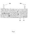
- FIGS. 1 and 2 depict a rough schematic top view of an inventive perforation grid in a superconducting film 12 , 22 .
- the rows between contacts 14 a , 14 b or 24 a , 24 b are determinant for DC signal development.
- I indicates the AC current and F L the Lorentz force.
- the double arrows indicate the direction of the AC current or the Lorentz force based on an applied HF signal.
- the guided motion of the vortices is indicated with v.
- the dotted arrow consequently indicates the direction of the preferential guided motion of the vortices in the superconducting film.
- the interval between the perforations 13 is constant within the vertical rows in the direction of motion of the vortices from perforation edge to perforation edge and can range from 0.5 to 20 ⁇ m.
- the interval between the vertical rows can vary between 1 and 500 ⁇ m.
- the perforation size can be between about 0.5 and 50 ⁇ m in diameter.
- the interval between the triangular perforations 23 is constant within the vertical rows from perforation edge to perforation edge and can be between about 0.5 and 20 ⁇ m.
- the interval between the rows themselves can vary from 1 to 500 ⁇ m.
- the perforation size is about 0.5 to 20 ⁇ m.
- FIG. 3 depicts different perforation grids connected in series from the input 35 a to the output 35 b for simultaneously filtering different frequency contributions of an HF signal. Dotted lines delimit from one another the sections in the superconducting film that form the vortex diodes 32 ′, 32 ′′, 32 ⁇ ′′. In section 32 ′ there are seven rows of triangular perforations between the DC detectors, and in each of sections 32 ′′ and 32 ′′′ there are eight vertical rows thereof.
- the interval between the perforations within the vertical rows from perforation edge to perforation edge in sections 32 ′, 32 ′′ and 32 ′′′ can vary between 0.5 and 20 ⁇ m.
- the interval between the rows themselves is about 1 to 500 ⁇ m.
- Sections 32 ′, 32 ′′ and 32 ′′′ each form a vortex diode so that in the present case a total of three vortex diodes are provided for filtering three frequency contributions.
- each interval between the triangular perforations 33 ′, 33 ′′ and 33 ′′′ decreases in the vertically arranged rows from section 32 ′ through 32 ′′ to 32 ′′′ and thus more perforations are arranged in each row.
- Five perforations per row are depicted in section 32 ′, 7 perforations per row in section 32 ′′, and 9 perforations per row in section 32 ′′′.
- a filter is created by adding perforations and rows of perforations.
- frequency contributions in the superconducting stripline are fed into the input 35 a and flow through the different diodes to the output 35 b , e.g. a ground.
- a frequency contribution is filtered out in each of the different sections 32 ′, 32 ′′, 32 ′′′ and detected and measured (not shown) via the DC contacts 34 a ′ and 34 b ′ or 34 a ′′ and 34 b ′′ or 34 a ′′′ and 34 b′′′.
- FIG. 4 is a schematic depiction of a filter based on vortex diodes having superconducting films 42 ′, 42 ′′, 42 ′′′.
- the signal depicted by the horizontal arrow, is received by means of an antenna 45 and optionally amplified by an amplifier 41 .
- the signal is now forwarded to vortex diodes having superconducting films 42 ′, 42 ′′ and 42 ′′′.
- FIG. 5 depicts another option for embodying a vortex diode.
- it is an asymmetrical arrangement of identical perforations 53 (e.g., round perforations; non-equilateral, isosceles triangular perforations) that is determinant for the preferred direction in which the vortices move in the stripline or film 52 , rather than the asymmetrical shape of perforations or antidots as such.
- the vortices follow the Lorentz force FL, but due to the wandering arrangement of the perforations 53 are forced to move preferentially along the dotted perforation rows.
- the substrate (not shown) comprises an HF capable material, e.g. made of single crystals including sapphire, LaAlO 3 , MgO, or silicon, the thickness of which should be selected according to impedance (generally 50 ⁇ ).
- HF capable material e.g. made of single crystals including sapphire, LaAlO 3 , MgO, or silicon, the thickness of which should be selected according to impedance (generally 50 ⁇ ).
- the average distance r, a vortex covers within a half wave (positive or negative current cycle) of the HF current is proportional to the amplitude of the signal (I max ) and the time ⁇ , during which the current is present, that is, the time of the half phase.
- the distance is inversely proportional to the frequency, r v ⁇ I/f.
- the distance traveled is inversely proportional to the frequency, at a given signal amplitude there is a maximum signal amplitude up to which vortices can travel from one antidot to another. Adding the frequency leads to an HF signal, and thus to an HF current in the conductor.
- the latter exerts a Lorentz force on the vortices using the interaction with the magnetic field in the vortex. Due to the small lower critical fields Bc, and the demagnetization effect in planar superconductors, even the smallest fields lead to significant vortex densities, earth fields normally being adequate.
- the directed motion of the vortices is induced inter alia by interaction between the applied current and the magnetic field of the vortex. The vortices interact with the current.
- a DC signal only occurs when a signal is injected that has adequate amplitude and has a frequency that is small enough.
- the inventive filters it is possible e.g. to filter frequencies from about 1 MHz to 100 GHz and convert them immediately to a DC signal.
Landscapes
- Engineering & Computer Science (AREA)
- Manufacturing & Machinery (AREA)
- Superconductor Devices And Manufacturing Methods Thereof (AREA)
- Superconductors And Manufacturing Methods Therefor (AREA)
- Solid State Image Pick-Up Elements (AREA)
Applications Claiming Priority (4)
| Application Number | Priority Date | Filing Date | Title |
|---|---|---|---|
| DE102005032422A DE102005032422B4 (de) | 2005-07-12 | 2005-07-12 | Anordnung aus Träger und supraleitendem Film, Vortexdiode, umfassend eine derartige Anordnung sowie Verwendung von Vortexdioden für Filter |
| DE102005032422 | 2005-07-12 | ||
| DE102005032422.3 | 2005-07-12 | ||
| PCT/DE2006/001112 WO2007006252A1 (de) | 2005-07-12 | 2006-06-28 | Anordnung aus träger und supraleitendem film, vortexdiode, umfassend eine derartige anordnung sowie verwendung von vortexdioden für filter |
Publications (2)
| Publication Number | Publication Date |
|---|---|
| US20090027140A1 US20090027140A1 (en) | 2009-01-29 |
| US8822979B2 true US8822979B2 (en) | 2014-09-02 |
Family
ID=37420759
Family Applications (1)
| Application Number | Title | Priority Date | Filing Date |
|---|---|---|---|
| US11/988,522 Expired - Fee Related US8822979B2 (en) | 2005-07-12 | 2006-06-28 | Arrangement comprising a support and super-conductive film, vortex diode comprising said type of arrangement and use of vortex diodes for filters |
Country Status (5)
| Country | Link |
|---|---|
| US (1) | US8822979B2 (de) |
| EP (1) | EP1902479B1 (de) |
| AT (1) | ATE470956T1 (de) |
| DE (2) | DE102005032422B4 (de) |
| WO (1) | WO2007006252A1 (de) |
Citations (5)
| Publication number | Priority date | Publication date | Assignee | Title |
|---|---|---|---|---|
| US4608296A (en) * | 1983-12-06 | 1986-08-26 | Energy Conversion Devices, Inc. | Superconducting films and devices exhibiting AC to DC conversion |
| US4828931A (en) | 1987-03-23 | 1989-05-09 | Osaka Prefecture | Superconductor for magnetic field shielding |
| DE19927661A1 (de) | 1998-06-22 | 1999-12-23 | Forschungszentrum Juelich Gmbh | Anordnung aus Träger und supraleitendem Film |
| US6569811B1 (en) * | 1997-06-11 | 2003-05-27 | University Of Cincinnati | Enhancement of JC in oxide superconductors |
| US20090048113A1 (en) * | 2001-06-19 | 2009-02-19 | Japan Science And Technology Agency | Superconducting thin film having columnar pinning centers utilizing nano dots and method of making the same |
-
2005
- 2005-07-12 DE DE102005032422A patent/DE102005032422B4/de not_active Expired - Lifetime
-
2006
- 2006-06-28 US US11/988,522 patent/US8822979B2/en not_active Expired - Fee Related
- 2006-06-28 DE DE502006007178T patent/DE502006007178D1/de active Active
- 2006-06-28 EP EP06761719A patent/EP1902479B1/de not_active Not-in-force
- 2006-06-28 WO PCT/DE2006/001112 patent/WO2007006252A1/de not_active Ceased
- 2006-06-28 AT AT06761719T patent/ATE470956T1/de active
Patent Citations (8)
| Publication number | Priority date | Publication date | Assignee | Title |
|---|---|---|---|---|
| US4608296A (en) * | 1983-12-06 | 1986-08-26 | Energy Conversion Devices, Inc. | Superconducting films and devices exhibiting AC to DC conversion |
| US4828931A (en) | 1987-03-23 | 1989-05-09 | Osaka Prefecture | Superconductor for magnetic field shielding |
| US6569811B1 (en) * | 1997-06-11 | 2003-05-27 | University Of Cincinnati | Enhancement of JC in oxide superconductors |
| DE19927661A1 (de) | 1998-06-22 | 1999-12-23 | Forschungszentrum Juelich Gmbh | Anordnung aus Träger und supraleitendem Film |
| US6175749B1 (en) | 1998-06-22 | 2001-01-16 | Forschungszentrum Julich Gmbh | Assembly of carrier and superconductive film |
| US6345190B1 (en) | 1998-06-22 | 2002-02-05 | Forschungszentrum Julich Gmbh | Assembly of carrier and superconductive film |
| US6345189B1 (en) | 1998-06-22 | 2002-02-05 | Forschungszentrum Julich Gmbh | Assembly of carrier and superconductive film |
| US20090048113A1 (en) * | 2001-06-19 | 2009-02-19 | Japan Science And Technology Agency | Superconducting thin film having columnar pinning centers utilizing nano dots and method of making the same |
Non-Patent Citations (12)
| Title |
|---|
| Hoffmann A et al: "Periodic vortex pinning with magnetic and nonmagnetic dots: The influence of size" Physical Review B (Condensed Matter) APS Through AIP USA, vo. 61, No. 10, Mar. 1, 2000, pp. 6958-6965, XP002408772 ISSN: 0163-1829-p. 6958, paragraph 1-p. 6959, paragraph 1. |
| Hoffmann A et al: "Periodic vortex pinning with magnetic and nonmagnetic dots: The influence of size" Physical Review B (Condensed Matter) APS Through AIP USA, vo. 61, No. 10, Mar. 1, 2000, pp. 6958-6965, XP002408772 ISSN: 0163-1829—p. 6958, paragraph 1-p. 6959, paragraph 1. |
| Van Look L et al: "Anisotropic vortex pinning by a square array of rectangular antidots" Physica C, North-Holland Publishing, Amsterdam, NL, vol. 369, No. 1-4, Mar. 15, 2002, pp. 113-117, XP004339833 ISSN: 0921-4534-the whole document. |
| Van Look L et al: "Anisotropic vortex pinning by a square array of rectangular antidots" Physica C, North-Holland Publishing, Amsterdam, NL, vol. 369, No. 1-4, Mar. 15, 2002, pp. 113-117, XP004339833 ISSN: 0921-4534—the whole document. |
| Villegas J E et al: "A superconducting reversible rectifier that controls the motion of magnetic flux quanta" Science American Assoc. Adv. Sci USA, vol. 302, No. 5648, Nov. 14, 2003, pp. 11-88-1191, XP002408726 ISSN: 0036-8075-the whole document. |
| Villegas J E et al: "Experimental ratchet effect in superconducting films with periodic arrays of aymmetric potentials" Physical Review B (Condensed Matter and Materials Physics) APS Through AIP USA, vol. 71, No. 2, Jan. 1, 2005, pp. 245191-245195, XP002408727 ISSN: 0163-1829-p. 0245191, paragraph 1-p. 0246193, paragraph 1. |
| Villegas J E et al: "A superconducting reversible rectifier that controls the motion of magnetic flux quanta" Science American Assoc. Adv. Sci USA, vol. 302, No. 5648, Nov. 14, 2003, pp. 11-88-1191, XP002408726 ISSN: 0036-8075—the whole document. |
| Villegas J E et al: "Experimental ratchet effect in superconducting films with periodic arrays of aymmetric potentials" Physical Review B (Condensed Matter and Materials Physics) APS Through AIP USA, vol. 71, No. 2, Jan. 1, 2005, pp. 245191-245195, XP002408727 ISSN: 0163-1829—p. 0245191, paragraph 1-p. 0246193, paragraph 1. |
| Woerdenweber, R. et al.; "Vortez lattice matching effects and 1/f-noise reduction in HTS films and devices equipped with regular arrays of artificial defects", Physica C, 332, (2000), pp. 27-34. |
| Woerdenweber, R. et al.; "Vortez lattice matching effects and 1/ƒ-noise reduction in HTS films and devices equipped with regular arrays of artificial defects", Physica C, 332, (2000), pp. 27-34. |
| Wordenweber R et al: "Guided vortex motion in high-Tc superconducting thin films and devices with special arrangements of artificial defects" Physica C, North-Holland Publishing, Amsterdam, NL, vol. 404, No. 11-4, May 1, 2004, pp. 421-425, XP004503420 ISSN: 0921-4534-the whole document. |
| Wordenweber R et al: "Guided vortex motion in high-Tc superconducting thin films and devices with special arrangements of artificial defects" Physica C, North-Holland Publishing, Amsterdam, NL, vol. 404, No. 11-4, May 1, 2004, pp. 421-425, XP004503420 ISSN: 0921-4534—the whole document. |
Also Published As
| Publication number | Publication date |
|---|---|
| ATE470956T1 (de) | 2010-06-15 |
| EP1902479B1 (de) | 2010-06-09 |
| DE102005032422A1 (de) | 2007-02-01 |
| DE502006007178D1 (de) | 2010-07-22 |
| EP1902479A1 (de) | 2008-03-26 |
| DE102005032422B4 (de) | 2008-06-26 |
| US20090027140A1 (en) | 2009-01-29 |
| WO2007006252A1 (de) | 2007-01-18 |
Similar Documents
| Publication | Publication Date | Title |
|---|---|---|
| Annunziata et al. | Tunable superconducting nanoinductors | |
| Hechtfischer et al. | Non-Josephson emission from intrinsic junctions in Bi 2 Sr 2 CaCu 2 O 8+ y: Cherenkov radiation by Josephson vortices | |
| Sonier et al. | Field induced reduction of the low-temperature superfluid density in YBa 2 Cu 3 O 6.95 | |
| US20170071082A1 (en) | Method and apparatus of implementing a magnetic shield flux sweeper | |
| Kakuyanagi et al. | Quasiparticle excitation in and around the vortex core of underdoped YBa 2 Cu 4 O 8 studied by site-selective NMR | |
| Uksusman et al. | Voltage response of current carrying Y–Ba–Cu–O tapes to alternating magnetic fields | |
| Hogg et al. | Vortex channeling and the voltage–current characteristics of YBa 2 Cu 3 O 7 low-angle grain boundaries | |
| Irie et al. | Microwave response of intrinsic Josephson junctions in BSCCO single crystals | |
| Cadorim et al. | Harnessing the superconducting diode effect through inhomogeneous magnetic fields | |
| Geng et al. | Time-varying magnetic field induced electric field across a current-transporting type-II superconducting loop: beyond dynamic resistance effect | |
| Wang et al. | Three-dimensional arrays of BiSrCaCuO-2212 intrinsic Josephson junctions and zero-crossing Shapiro steps at 760 GHz | |
| US8822979B2 (en) | Arrangement comprising a support and super-conductive film, vortex diode comprising said type of arrangement and use of vortex diodes for filters | |
| Chesca et al. | d-wave induced zero-field resonances in dc π-superconducting quantum interference devices | |
| Chesca | Magnetic field dependencies of the critical current and of the resonant modes of dc SQUIDs fabricated from superconductors with s+ id order‐parameter symmetries | |
| US7521708B1 (en) | High sensitivity ring-SQUID magnetic sensor | |
| DE19927661B4 (de) | Anordnung aus Träger und supraleitendem Film | |
| Al-Qurainy et al. | Large artificial ferromagnetic dot arrays for the critical current enhancement in superconducting YBa2Cu3O 7− δ thin films | |
| Volpini et al. | Electromagnetic study of a round coil superferric magnet | |
| Jones et al. | Changing the Critical Current Density and Magnetic Properties of YBa $ _2 $ Cu $ _3 $ O $ _7 $ by Using Large Antidots | |
| Yamani et al. | NMR evidence for Friedel-like oscillations in the CuO chains of ortho-II YBa 2 Cu 3 O 6.5 | |
| Shulga et al. | Observation of individual vortex penetration in a coplanar superconducting resonator | |
| US11626227B2 (en) | Apparatuses and methods for increasing magnetic flux density using superconductors | |
| Tai et al. | MgB 2 nonlinear properties investigated under localized high rf magnetic field excitation | |
| Cristiano et al. | The role of the geometry in superconducting tunnel junction detectors | |
| Zhang | Self-consistent study of the Josephson effect for the d-wave superconductor-insulator-superconductor junction |
Legal Events
| Date | Code | Title | Description |
|---|---|---|---|
| AS | Assignment |
Owner name: FORSCHUNGSZENTRUM JUELICH GMBH, GERMANY Free format text: ASSIGNMENT OF ASSIGNORS INTEREST;ASSIGNOR:WOERDENWEBER, ROGER;REEL/FRAME:020444/0589 Effective date: 20080107 |
|
| FEPP | Fee payment procedure |
Free format text: MAINTENANCE FEE REMINDER MAILED (ORIGINAL EVENT CODE: REM.) |
|
| LAPS | Lapse for failure to pay maintenance fees |
Free format text: PATENT EXPIRED FOR FAILURE TO PAY MAINTENANCE FEES (ORIGINAL EVENT CODE: EXP.); ENTITY STATUS OF PATENT OWNER: LARGE ENTITY |
|
| STCH | Information on status: patent discontinuation |
Free format text: PATENT EXPIRED DUE TO NONPAYMENT OF MAINTENANCE FEES UNDER 37 CFR 1.362 |
|
| FP | Lapsed due to failure to pay maintenance fee |
Effective date: 20180902 |