US8819931B2 - Enhanced-reliability printed circuit board for tight-pitch components - Google Patents
Enhanced-reliability printed circuit board for tight-pitch components Download PDFInfo
- Publication number
- US8819931B2 US8819931B2 US12/173,795 US17379508A US8819931B2 US 8819931 B2 US8819931 B2 US 8819931B2 US 17379508 A US17379508 A US 17379508A US 8819931 B2 US8819931 B2 US 8819931B2
- Authority
- US
- United States
- Prior art keywords
- angle
- panel
- printed circuit
- edges
- circuit board
- Prior art date
- Legal status (The legal status is an assumption and is not a legal conclusion. Google has not performed a legal analysis and makes no representation as to the accuracy of the status listed.)
- Active, expires
Links
Images


Classifications
-
- H—ELECTRICITY
- H05—ELECTRIC TECHNIQUES NOT OTHERWISE PROVIDED FOR
- H05K—PRINTED CIRCUITS; CASINGS OR CONSTRUCTIONAL DETAILS OF ELECTRIC APPARATUS; MANUFACTURE OF ASSEMBLAGES OF ELECTRICAL COMPONENTS
- H05K1/00—Printed circuits
- H05K1/02—Details
- H05K1/03—Use of materials for the substrate
- H05K1/0313—Organic insulating material
- H05K1/0353—Organic insulating material consisting of two or more materials, e.g. two or more polymers, polymer + filler, + reinforcement
- H05K1/0366—Organic insulating material consisting of two or more materials, e.g. two or more polymers, polymer + filler, + reinforcement reinforced, e.g. by fibres, fabrics
-
- H—ELECTRICITY
- H05—ELECTRIC TECHNIQUES NOT OTHERWISE PROVIDED FOR
- H05K—PRINTED CIRCUITS; CASINGS OR CONSTRUCTIONAL DETAILS OF ELECTRIC APPARATUS; MANUFACTURE OF ASSEMBLAGES OF ELECTRICAL COMPONENTS
- H05K1/00—Printed circuits
- H05K1/02—Details
- H05K1/0213—Electrical arrangements not otherwise provided for
- H05K1/0254—High voltage adaptations; Electrical insulation details; Overvoltage or electrostatic discharge protection ; Arrangements for regulating voltages or for using plural voltages
- H05K1/0256—Electrical insulation details, e.g. around high voltage areas
-
- H—ELECTRICITY
- H05—ELECTRIC TECHNIQUES NOT OTHERWISE PROVIDED FOR
- H05K—PRINTED CIRCUITS; CASINGS OR CONSTRUCTIONAL DETAILS OF ELECTRIC APPARATUS; MANUFACTURE OF ASSEMBLAGES OF ELECTRICAL COMPONENTS
- H05K2201/00—Indexing scheme relating to printed circuits covered by H05K1/00
- H05K2201/02—Fillers; Particles; Fibers; Reinforcement materials
- H05K2201/0275—Fibers and reinforcement materials
- H05K2201/029—Woven fibrous reinforcement or textile
-
- H—ELECTRICITY
- H05—ELECTRIC TECHNIQUES NOT OTHERWISE PROVIDED FOR
- H05K—PRINTED CIRCUITS; CASINGS OR CONSTRUCTIONAL DETAILS OF ELECTRIC APPARATUS; MANUFACTURE OF ASSEMBLAGES OF ELECTRICAL COMPONENTS
- H05K2201/00—Indexing scheme relating to printed circuits covered by H05K1/00
- H05K2201/07—Electric details
- H05K2201/0753—Insulation
- H05K2201/0769—Anti metal-migration, e.g. avoiding tin whisker growth
-
- H—ELECTRICITY
- H05—ELECTRIC TECHNIQUES NOT OTHERWISE PROVIDED FOR
- H05K—PRINTED CIRCUITS; CASINGS OR CONSTRUCTIONAL DETAILS OF ELECTRIC APPARATUS; MANUFACTURE OF ASSEMBLAGES OF ELECTRICAL COMPONENTS
- H05K2201/00—Indexing scheme relating to printed circuits covered by H05K1/00
- H05K2201/09—Shape and layout
- H05K2201/09209—Shape and layout details of conductors
- H05K2201/09218—Conductive traces
- H05K2201/09227—Layout details of a plurality of traces, e.g. escape layout for Ball Grid Array [BGA] mounting
-
- Y—GENERAL TAGGING OF NEW TECHNOLOGICAL DEVELOPMENTS; GENERAL TAGGING OF CROSS-SECTIONAL TECHNOLOGIES SPANNING OVER SEVERAL SECTIONS OF THE IPC; TECHNICAL SUBJECTS COVERED BY FORMER USPC CROSS-REFERENCE ART COLLECTIONS [XRACs] AND DIGESTS
- Y10—TECHNICAL SUBJECTS COVERED BY FORMER USPC
- Y10T—TECHNICAL SUBJECTS COVERED BY FORMER US CLASSIFICATION
- Y10T29/00—Metal working
- Y10T29/49—Method of mechanical manufacture
- Y10T29/49002—Electrical device making
- Y10T29/49117—Conductor or circuit manufacturing
- Y10T29/49124—On flat or curved insulated base, e.g., printed circuit, etc.
- Y10T29/49126—Assembling bases
-
- Y—GENERAL TAGGING OF NEW TECHNOLOGICAL DEVELOPMENTS; GENERAL TAGGING OF CROSS-SECTIONAL TECHNOLOGIES SPANNING OVER SEVERAL SECTIONS OF THE IPC; TECHNICAL SUBJECTS COVERED BY FORMER USPC CROSS-REFERENCE ART COLLECTIONS [XRACs] AND DIGESTS
- Y10—TECHNICAL SUBJECTS COVERED BY FORMER USPC
- Y10T—TECHNICAL SUBJECTS COVERED BY FORMER US CLASSIFICATION
- Y10T29/00—Metal working
- Y10T29/49—Method of mechanical manufacture
- Y10T29/49002—Electrical device making
- Y10T29/49117—Conductor or circuit manufacturing
- Y10T29/49124—On flat or curved insulated base, e.g., printed circuit, etc.
- Y10T29/49147—Assembling terminal to base
-
- Y—GENERAL TAGGING OF NEW TECHNOLOGICAL DEVELOPMENTS; GENERAL TAGGING OF CROSS-SECTIONAL TECHNOLOGIES SPANNING OVER SEVERAL SECTIONS OF THE IPC; TECHNICAL SUBJECTS COVERED BY FORMER USPC CROSS-REFERENCE ART COLLECTIONS [XRACs] AND DIGESTS
- Y10—TECHNICAL SUBJECTS COVERED BY FORMER USPC
- Y10T—TECHNICAL SUBJECTS COVERED BY FORMER US CLASSIFICATION
- Y10T29/00—Metal working
- Y10T29/49—Method of mechanical manufacture
- Y10T29/49002—Electrical device making
- Y10T29/49117—Conductor or circuit manufacturing
- Y10T29/49124—On flat or curved insulated base, e.g., printed circuit, etc.
- Y10T29/49155—Manufacturing circuit on or in base
- Y10T29/49165—Manufacturing circuit on or in base by forming conductive walled aperture in base
-
- Y—GENERAL TAGGING OF NEW TECHNOLOGICAL DEVELOPMENTS; GENERAL TAGGING OF CROSS-SECTIONAL TECHNOLOGIES SPANNING OVER SEVERAL SECTIONS OF THE IPC; TECHNICAL SUBJECTS COVERED BY FORMER USPC CROSS-REFERENCE ART COLLECTIONS [XRACs] AND DIGESTS
- Y10—TECHNICAL SUBJECTS COVERED BY FORMER USPC
- Y10T—TECHNICAL SUBJECTS COVERED BY FORMER US CLASSIFICATION
- Y10T428/00—Stock material or miscellaneous articles
- Y10T428/24—Structurally defined web or sheet [e.g., overall dimension, etc.]
- Y10T428/24802—Discontinuous or differential coating, impregnation or bond [e.g., artwork, printing, retouched photograph, etc.]
- Y10T428/24917—Discontinuous or differential coating, impregnation or bond [e.g., artwork, printing, retouched photograph, etc.] including metal layer
Definitions
- This disclosure generally relates to circuit boards, and more specifically relates to printed circuit boards for tight-pitch components.
- Printed circuit boards are commonly constructed of glass cloth impregnated with various epoxy resins.
- the glass cloth is typically constructed of bundles of glass fibers woven together in an X-Y orthogonal fashion, with the bundles being perpendicular to each other.
- the epoxy/glass substrate is laminated to copper foil, forming “cores” which are subsequently etched to form the desired features. These cores are then laminated together using partially cured epoxy/glass layers with temperature and pressure, causing the resin to flow between layers to form a robust composite structure.
- CAF growth results when a pathway exists along or within the individual glass fibers within the printed circuit board where a conductive path may form.
- a conductive filament of copper salts may grow along one or more of the glass fibers when there is both voltage and moisture present, such as when equipment operates in a high humidity environment.
- the conductive filament may eventually grow to a length sufficient to short together two features that should not be connected, such as adjacent plated-through holes in the printed circuit board, causing the printed circuit board to fail.
- CAF growth has been attributed to one or more of several possible scenarios, including: 1) hollow glass fibers as a result of bubbles in the liquid glass during the extrusion process that forms the glass fibers; 2) insufficient binding of the resin to the glass fibers, which may occur when the resin is initially bound to the glass fibers, or may occur only after exposure to thermal cycles, such as those that occur during normal system operation; 3) insufficient impregnation of the resin into the bundles of glass fibers, leaving small open tracks where multiple glass fibers meet (sometimes called a “triple point”). Note that CAF growth is well-understood in the art, and its underlying mechanisms therefore are not discussed further here.
- CAF growth has been documented and understood for some time, but in the past CAF growth has not been a significant reliability concern for printed circuit boards because the time required for a conductive filament to grow between features on a printed circuit board typically has been greater than the life expectancy of the system in which the printed circuit board is located.
- the spacing between conductive leads or contacts on electronic components (referred to in the art as “pitch”) continues to shrink.
- the time it takes for a CAF growth to bridge two features on a printed circuit board shrinks correspondingly.
- the CAF growth With the advent of sub-1 mm and lower pitch components, the CAF growth has now been shown to occur within the time frame of system life expectations. As a result, CAF growth becomes a reliability concern for printed circuit boards with tight-pitch components.
- a printed circuit board is fabricated such that component contacts for tight-pitch components are at an angle with respect to the bundles of glass fibers in the epoxy-glass printed circuit board such that adjacent component contacts do not contact the same bundle of glass fibers.
- This angle may be accomplished by manufacturing a printed circuit board panel with the glass fibers at an angle with respect to its edges. Parts and components are then laid out on the panel in an X-Y orientation with respect to the panel's edges. In the alternative, this angle may be accomplished by placing parts on a printed circuit board panel at an angle with respect to the edges of the panel that has a traditional X-Y orthogonal weave of glass fiber bundles. Components are then laid out on the parts in an X-Y orientation with respect to the part's edges.
- This angle may also be accomplished by starting with a traditional panel that has an X-Y orthogonal weave of glass fiber bundles, laying out parts on the panel along the X-Y weave, then placing components on the parts at an angle with respect to the edges of the parts.
- FIG. 1 is a known method for manufacturing panels, laying out parts, and laying out components on printed circuit board panels;
- FIG. 2 is a simplified example showing a panel, parts, and components that are all laid out in the same X-Y orientation as the underlying orthogonal weave of the glass fiber bundles in the printed circuit board;
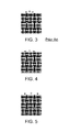
- FIG. 3 is a diagram showing a potential path for CAF growth between plated-through holes in a known printed circuit board
- FIG. 4 is a diagram that shows how the length of a path for CAF growth can be lengthened by placing a component at an angle with respect to the underlying X-Y orientation of the glass fiber bundles in the printed circuit board;
- FIG. 5 is a diagram that illustrates that the length of the path for CAF growth can be lengthened even more by providing a different angle for the component plated-through holes with respect to the underlying X-Y orientation of the glass fiber bundles in the printed circuit board;
- FIG. 6 is a flow diagram of a method for laying out components on a printed circuit board at an angle with respect to the X-Y orientation of the glass fiber bundles in the printed circuit board;
- FIG. 7 is a flow diagram of one specific way of laying out components on a printed circuit board at an angle with respect to the X-Y orientation of the glass fiber bundles in the printed circuit board by placing the components at an angle with respect to the X-Y orientation of parts on a panel;
- FIG. 8 is a diagram that illustrates a possible result of method 610 A in FIG. 7 ;
- FIG. 9 is a flow diagram of one specific way of laying out components on a printed circuit board at an angle with respect to the X-Y orientation of the glass fiber bundles in the printed circuit board by laying out parts on a panel at an angle with respect to the X-Y orientation of the panel;
- FIG. 10 is a diagram that illustrates a possible result of method 610 B in FIG. 9 ;
- FIG. 11 is a flow diagram of one specific way of laying out components on a printed circuit board at an angle with respect to the X-Y orientation of the glass fiber bundles in the printed circuit board by manufacturing a panel that has glass fiber bundles at an angle with respect to its edges, then laying out parts and components on the panel in alignment with the edges of the panel;
- FIG. 12 is a diagram that illustrates a possible result of method 610 C in FIG. 11 ;
- FIG. 13 is a diagram showing angled paths that result in adjacent features in a printed circuit board not being connected to the same bundle of glass fibers when the adjacent features are arranged in an orthogonal array as shown;
- FIG. 14 is a diagram showing angled paths that result in adjacent features in a printed circuit board not being connected to the same bundle of glass fibers when the adjacent features are arranged in an interstitial array as shown;
- FIG. 15 is a diagram showing angles for a path in an orthogonal array such as that shown in FIG. 13 ;
- FIG. 16 shows formulas for calculating the angles for the path shown in FIG. 15 .
- a printed circuit board is fabricated such that a plurality of component contacts on the printed circuit board are disposed at an angle with respect to the X-Y array of glass fiber bundles in the substrate of the printed circuit board so that adjacent component contacts will not contact the same glass fiber bundle.
- the result is that paths between component contacts along the same glass fiber bundle are longer than the component pitch, thereby minimizing the likelihood of Conductive Anodic Filament (CAF) growth causing a failure in the printed circuit board.
- CAF Conductive Anodic Filament
- a prior art method 100 for fabricating a printed circuit board begins by manufacturing a circuit board panel with glass fiber bundles in an orthogonal X-Y matrix (step 110 ). The components are then laid out on the parts in the same X-Y orientation (step 120 ). One or more parts are then laid out on the panel in the same X-Y orientation (step 130 ). This means that the parts have edges that are parallel to and perpendicular to the edges of the panel.
- the result is a panel with parts and components that all align with the X-Y orientation of the glass fiber bundles in the underlying panel, as shown by sample panel 200 in FIG. 2 , which is shown with eight identical parts with edges parallel and perpendicular to the panel edges, where each part has a component C 1 that has contacts that are also aligned parallel and perpendicular to the part edges.
- Conductive Anodic Filament (CAF) growth is a known failure mechanism for printed circuit boards. Copper salts may form along a bundle of glass fibers in the presence of voltage and moisture, and may eventually form a conductive bridge between component contacts that causes a failure of the printed circuit board assembly.
- the term “pitch” herein refers to spacing between component contacts. As the pitch continues to shrink, the length of the path between adjacent component contacts is reduced, thereby reducing the time required for a conductive bridge to form between component contacts that contact the same glass fiber bundle in the printed circuit board. With component pitches of 1.0 mm or less, the time required for a conductive bridge to form between adjacent component contacts via CAF growth may be less than the anticipated life of the electronic assembly, which can result in premature failure of the electronic assembly.
- FIG. 3 shows some component contacts in the form of plated-through holes in a substrate that includes a woven matrix of glass fiber bundles in an X-Y arrangement as shown. Because adjacent component contacts are aligned on the same glass fiber bundle, the path along a glass fiber bundle where CAF growth may occur is governed by the pitch of the component contacts. Thus, in FIG. 3 , the distance m between plated through holes is the distance where CAF growth can cause a failure in the printed circuit board assembly.
- An enhanced-reliability circuit board may be fabricated by aligning component contacts so that adjacent component contacts do not contact the same glass fiber bundle in the printed circuit board, as shown in FIGS. 4 and 5 .
- the angle shown in FIG. 4 results in a distance n that is larger than distance m in FIG. 3 for the same pitch components.
- the path shown in FIG. 4 is approximately 40% longer than the path shown in FIG. 3 .
- Adjusting the angle of the component contacts with respect to the X-Y matrix of glass fiber bundles may further increase the distance between component contacts that contact the same glass fiber bundle, as shown in FIG. 5 .
- the distance o along a glass fiber bundle is greater than distance n in FIG. 4 and greater than distance m in FIG. 3 .
- angle In the broadest and strictest sense of the term “angle”, zero degrees and ninety degrees are angles. However, the angle herein that results in adjacent component contacts not contacting the same glass fiber bundle are non-zero and non-ninety degree angles.
- a method 600 includes the step of laying out components on parts at an angle with respect to the X-Y orientation of the glass fiber bundles in the printed circuit board so adjacent component contacts do not contact the same bundle of glass fibers (step 610 ).
- Step 610 may be accomplished in a number of different ways. Three of those ways are shown in FIGS. 7 , 9 and 11 , with the resulting structures shown in FIGS. 8 , 10 and 12 , respectively.
- a first method 610 A for performing step 610 in FIG. 6 begins by manufacturing a circuit board panel with the glass fiber bundles in a traditional X-Y matrix (step 710 ).
- the components on the individual parts are then laid out at an angle with respect to the X-Y orientation of the parts so adjacent component contacts do not make contact with the same bundle of glass fibers in the underlying substrate of the part and panel (step 720 ).
- Parts are then laid out on the panel in X-Y orientation (step 730 ). Note that all of the components need not be laid out at an angle. Tight-pitch components could be laid out at an angle while other components are laid out in X-Y orientation.
- the disclosure and claims herein express extend to laying out one or more components at an angle so that adjacent component contacts do not contact the same bundle of glass fibers. The result is shown graphically in FIG.
- FIG. 9 Another method 610 B for performing step 610 in FIG. 6 is shown in FIG. 9 .
- a circuit board panel is manufactured with glass fiber bundles in an X-Y matrix (step 710 ).
- the components are then laid out on the parts in an X-Y orientation with respect to the part edges (step 920 ).
- the parts are then laid out at an angle with respect to the X-Y orientation of the panel such that component contacts that are laid out in the following step do not contact the same bundle of glass fibers in the underlying substrate of the part and panel (step 930 ).
- This configuration is shown in FIG. 10 .
- the desired angle is achieved that assures that adjacent component contacts do not contact the same bundle of glass fibers in the underlying substrate of the part and panel.
- FIG. 11 Another method 610 C for performing step 610 in FIG. 6 is shown in FIG. 11 .
- a circuit board panel is manufactured with glass fiber bundles at an angle with respect to the edges of the panel so adjacent component contacts laid out in step 1130 do not contact the same bundle of glass fibers (step 1110 ).
- the components are then laid out on the parts in an X-Y orientation with respect to the edges of the parts (step 1120 ).
- the parts are then laid out in an X-Y orientation with respect to the edges of the panel (step 1130 ).
- FIG. 12 One way method 610 C could be achieved is shown in FIG. 12 , where a panel 1200 is cut from a large panel 1210 that has the glass fiber bundles in a traditional orthogonal X-Y matrix.
- FIG. 13 shows graphically paths that avoid contacts between adjacent component contacts in an orthogonal array of component contacts.
- FIG. 14 shows graphically paths that avoid contacts between adjacent component contacts in an interstitial array of component contacts. In both cases, the angle is preferably selected so that no bundle of glass fibers will contact two adjacent component contacts.
- the angle may be calculated as shown in FIGS. 15 and 16 .
- FIG. 15 we assume plated-through holes of diameter D are used, with a horizontal distance Ph between plated-through holes and a vertical distance Pv between plated-through holes. As shown by the lines extending from plated-through hole J in FIG. 15 , the angles of these lines define angles which will assure that adjacent component contacts do not contact the same glass fiber bundle.
- the angle A shown in FIG. 15 is computed as shown in FIG. 16 to be the arcsine of the diameter D of the plated through hole divided by the vertical distance Pv between the centers of the plated through holes.
- the angle B shown in FIG. 15 is computed as shown in FIG. 16 .
- the result is two angles that define an upper and lower bound for the angle at which component contacts are placed with respect to the orthogonal X-Y matrix of underlying glass fiber bundles in the printed circuit board substrate.
- the distance between component contacts along a glass fiber bundle will be maximized by selecting an angle that lies between angles A and B shown in FIG. 15 as computed in FIG. 16 .
- a printed circuit board provides enhanced reliability for tight-pitch components by assuring that adjacent component contacts do not contact the same glass fiber bundle in the underlying epoxy/glass substrate of the printed circuit board. By making sure that adjacent component contacts do not contact the same glass fiber bundle, the distance between component contacts along a glass fiber bundle is increased, thereby reducing the likelihood of failure due to CAF growth along the glass fiber bundle.
Landscapes
- Engineering & Computer Science (AREA)
- Microelectronics & Electronic Packaging (AREA)
- Manufacturing Of Printed Wiring (AREA)
- Production Of Multi-Layered Print Wiring Board (AREA)
- Printing Elements For Providing Electric Connections Between Printed Circuits (AREA)
Abstract
Description
Claims (8)
ArcSin(D/Pv)
ArcCos(D/Sqrt(Pv 2 +Ph 2))+ArcTan(Pv/Ph)−90°
ArcSin(D/Pv); and
ArcCos(D/Sqrt(Pv 2 +Ph 2))+ArcTan(Pv/Ph)−90°
Priority Applications (1)
| Application Number | Priority Date | Filing Date | Title |
|---|---|---|---|
| US12/173,795 US8819931B2 (en) | 2006-07-14 | 2008-07-15 | Enhanced-reliability printed circuit board for tight-pitch components |
Applications Claiming Priority (2)
| Application Number | Priority Date | Filing Date | Title |
|---|---|---|---|
| US11/457,492 US7615705B2 (en) | 2006-07-14 | 2006-07-14 | Enhanced-reliability printed circuit board for tight-pitch components |
| US12/173,795 US8819931B2 (en) | 2006-07-14 | 2008-07-15 | Enhanced-reliability printed circuit board for tight-pitch components |
Related Parent Applications (1)
| Application Number | Title | Priority Date | Filing Date |
|---|---|---|---|
| US11/457,492 Division US7615705B2 (en) | 2006-07-14 | 2006-07-14 | Enhanced-reliability printed circuit board for tight-pitch components |
Publications (2)
| Publication Number | Publication Date |
|---|---|
| US20080271314A1 US20080271314A1 (en) | 2008-11-06 |
| US8819931B2 true US8819931B2 (en) | 2014-09-02 |
Family
ID=38949622
Family Applications (2)
| Application Number | Title | Priority Date | Filing Date |
|---|---|---|---|
| US11/457,492 Active 2027-04-29 US7615705B2 (en) | 2006-07-14 | 2006-07-14 | Enhanced-reliability printed circuit board for tight-pitch components |
| US12/173,795 Active 2031-03-24 US8819931B2 (en) | 2006-07-14 | 2008-07-15 | Enhanced-reliability printed circuit board for tight-pitch components |
Family Applications Before (1)
| Application Number | Title | Priority Date | Filing Date |
|---|---|---|---|
| US11/457,492 Active 2027-04-29 US7615705B2 (en) | 2006-07-14 | 2006-07-14 | Enhanced-reliability printed circuit board for tight-pitch components |
Country Status (2)
| Country | Link |
|---|---|
| US (2) | US7615705B2 (en) |
| CN (1) | CN101106862B (en) |
Families Citing this family (12)
| Publication number | Priority date | Publication date | Assignee | Title |
|---|---|---|---|---|
| JP5018840B2 (en) * | 2009-07-27 | 2012-09-05 | 富士通株式会社 | Coupon board |
| JP2011029451A (en) * | 2009-07-27 | 2011-02-10 | Fujitsu Ltd | Printed circuit board, electronic apparatus, and method for manufacturing printed circuit board |
| CN102131339B (en) * | 2010-01-14 | 2013-06-05 | 鸿富锦精密工业(深圳)有限公司 | Printed circuit board |
| US8974888B2 (en) | 2011-08-30 | 2015-03-10 | International Business Machines Corporation | Preventing conductive anodic filament (CAF) formation by sealing discontinuities in glass fiber bundles |
| CN103364674B (en) * | 2012-03-30 | 2016-01-20 | 北大方正集团有限公司 | The decision method that conductive anodic filament lost efficacy |
| US9179556B2 (en) | 2012-08-03 | 2015-11-03 | Lenovo Enterprise Solutions (Singapore) Pte. Ltd. | Preventing the formation of conductive anodic filaments in a printed circuit board |
| CN103336019A (en) * | 2013-05-28 | 2013-10-02 | 麦可罗泰克(常州)产品服务有限公司 | Method for analyzing circuit board conductive anodic filament failure |
| US9456496B2 (en) | 2015-02-12 | 2016-09-27 | International Business Machines Corporation | Substrate containing low-Dk-core glass fibers having low dielectric constant (Dk) cores for use in printed circuit boards (PCBs), and method of making same |
| CN105357891A (en) * | 2015-11-09 | 2016-02-24 | 广东方大索正光电照明有限公司 | Method for printing electronic circuit on glass |
| US10212812B2 (en) | 2016-01-15 | 2019-02-19 | International Business Machines Corporation | Composite materials including filled hollow glass filaments |
| US10172243B2 (en) | 2016-11-14 | 2019-01-01 | International Business Machines Corporation | Printed circuit board and methods to enhance reliability |
| CN114828402A (en) * | 2022-04-14 | 2022-07-29 | 广东通元精密电路有限公司 | Hole wiring structure for improving CAF (computer aided design) between holes, design method, printed board and electronic product |
Citations (6)
| Publication number | Priority date | Publication date | Assignee | Title |
|---|---|---|---|---|
| US3371250A (en) | 1966-03-09 | 1968-02-27 | Southern Weaving Co | Woven circuit device |
| US4103102A (en) | 1976-07-01 | 1978-07-25 | Bell Telephone Laboratories, Incorporated | Reinforced flexible printed wiring board |
| US4980217A (en) | 1988-07-29 | 1990-12-25 | Grundfest Michael A | Printed circuit board fabrication |
| US5165166A (en) | 1987-09-29 | 1992-11-24 | Microelectronics And Computer Technology Corporation | Method of making a customizable circuitry |
| US5777855A (en) * | 1996-06-18 | 1998-07-07 | Eastman Kodak Company | Method and apparatus for connecting flexible circuits to printed circuit boards |
| US6949289B1 (en) * | 1998-03-03 | 2005-09-27 | Ppg Industries Ohio, Inc. | Impregnated glass fiber strands and products including the same |
Family Cites Families (2)
| Publication number | Priority date | Publication date | Assignee | Title |
|---|---|---|---|---|
| US5037691A (en) * | 1986-09-15 | 1991-08-06 | Compositech, Ltd. | Reinforced plastic laminates for use in the production of printed circuit boards and process for making such laminates and resulting products |
| US6613413B1 (en) * | 1999-04-26 | 2003-09-02 | International Business Machines Corporation | Porous power and ground planes for reduced PCB delamination and better reliability |
-
2006
- 2006-07-14 US US11/457,492 patent/US7615705B2/en active Active
-
2007
- 2007-05-16 CN CN200710102600.9A patent/CN101106862B/en active Active
-
2008
- 2008-07-15 US US12/173,795 patent/US8819931B2/en active Active
Patent Citations (6)
| Publication number | Priority date | Publication date | Assignee | Title |
|---|---|---|---|---|
| US3371250A (en) | 1966-03-09 | 1968-02-27 | Southern Weaving Co | Woven circuit device |
| US4103102A (en) | 1976-07-01 | 1978-07-25 | Bell Telephone Laboratories, Incorporated | Reinforced flexible printed wiring board |
| US5165166A (en) | 1987-09-29 | 1992-11-24 | Microelectronics And Computer Technology Corporation | Method of making a customizable circuitry |
| US4980217A (en) | 1988-07-29 | 1990-12-25 | Grundfest Michael A | Printed circuit board fabrication |
| US5777855A (en) * | 1996-06-18 | 1998-07-07 | Eastman Kodak Company | Method and apparatus for connecting flexible circuits to printed circuit boards |
| US6949289B1 (en) * | 1998-03-03 | 2005-09-27 | Ppg Industries Ohio, Inc. | Impregnated glass fiber strands and products including the same |
Also Published As
| Publication number | Publication date |
|---|---|
| US7615705B2 (en) | 2009-11-10 |
| CN101106862B (en) | 2012-09-26 |
| US20080271314A1 (en) | 2008-11-06 |
| US20080014419A1 (en) | 2008-01-17 |
| CN101106862A (en) | 2008-01-16 |
Similar Documents
| Publication | Publication Date | Title |
|---|---|---|
| US8819931B2 (en) | Enhanced-reliability printed circuit board for tight-pitch components | |
| US8493747B2 (en) | Flex-rigid wiring board and method for manufacturing the same | |
| JP5097827B2 (en) | Flex-rigid wiring board and electronic device | |
| CN102293069B (en) | Wiring board and method for manufacturing the same | |
| JP5085266B2 (en) | Wiring board and manufacturing method thereof | |
| KR101837435B1 (en) | Thermal management of printed circuit board components | |
| US4980217A (en) | Printed circuit board fabrication | |
| JP2013089902A (en) | Wiring substrate and manufacturing method of the same | |
| US6919635B2 (en) | High density microvia substrate with high wireability | |
| US8754333B2 (en) | Printed circuit board incorporating fibers | |
| JP5491026B2 (en) | Manufacturing method for constructing reinforcing core material in printed wiring board | |
| US8491739B2 (en) | Implementing interleaved-dielectric joining of multi-layer laminates | |
| HK1112553A (en) | Printed circuit board and its fabricating method | |
| US9049794B2 (en) | Wiring substrate and method for manufacturing the wiring substrate | |
| US6492007B1 (en) | Multi-layer printed circuit bare board enabling higher density wiring and a method of manufacturing the same | |
| JP2003069219A (en) | Method for designing through hole and printed wiring board | |
| KR20230018926A (en) | Circuit board | |
| JP4683736B2 (en) | Drilling method | |
| US20210385952A1 (en) | Resin flow restriction process and structure | |
| JP5082821B2 (en) | Through board | |
| JP2024102544A (en) | Wiring Board | |
| JP2008060119A (en) | Printed wiring board | |
| Navarro | Standardizing a Test Method for Conductive Anodic Filament Growth Failure | |
| KR100863305B1 (en) | Data recognition method in jumper structure | |
| JP2009021470A (en) | Circuit board |
Legal Events
| Date | Code | Title | Description |
|---|---|---|---|
| AS | Assignment |
Owner name: INTERNATIONAL BUSINESS MACHINES CORPORATION, NEW Y Free format text: ASSIGNMENT OF ASSIGNORS INTEREST;ASSIGNORS:CHAMBERLIN, BRUCE JOHN;FERRILL, MITCHELL G.;KRABBENHOFT, ROGER SCOTT;SIGNING DATES FROM 20060710 TO 20060712;REEL/FRAME:032775/0362 |
|
| STCF | Information on status: patent grant |
Free format text: PATENTED CASE |
|
| FEPP | Fee payment procedure |
Free format text: MAINTENANCE FEE REMINDER MAILED (ORIGINAL EVENT CODE: REM.) |
|
| FEPP | Fee payment procedure |
Free format text: SURCHARGE FOR LATE PAYMENT, LARGE ENTITY (ORIGINAL EVENT CODE: M1554); ENTITY STATUS OF PATENT OWNER: LARGE ENTITY |
|
| MAFP | Maintenance fee payment |
Free format text: PAYMENT OF MAINTENANCE FEE, 4TH YEAR, LARGE ENTITY (ORIGINAL EVENT CODE: M1551); ENTITY STATUS OF PATENT OWNER: LARGE ENTITY Year of fee payment: 4 |
|
| MAFP | Maintenance fee payment |
Free format text: PAYMENT OF MAINTENANCE FEE, 8TH YEAR, LARGE ENTITY (ORIGINAL EVENT CODE: M1552); ENTITY STATUS OF PATENT OWNER: LARGE ENTITY Year of fee payment: 8 |
|
| FEPP | Fee payment procedure |
Free format text: MAINTENANCE FEE REMINDER MAILED (ORIGINAL EVENT CODE: REM.); ENTITY STATUS OF PATENT OWNER: LARGE ENTITY |