US8803116B2 - Receiving circuit having a switch for changing the generated reference voltage to one of a first and a second threshold value - Google Patents
Receiving circuit having a switch for changing the generated reference voltage to one of a first and a second threshold value Download PDFInfo
- Publication number
- US8803116B2 US8803116B2 US13/412,462 US201213412462A US8803116B2 US 8803116 B2 US8803116 B2 US 8803116B2 US 201213412462 A US201213412462 A US 201213412462A US 8803116 B2 US8803116 B2 US 8803116B2
- Authority
- US
- United States
- Prior art keywords
- output
- switch
- reference voltage
- circuit
- circuit according
- Prior art date
- Legal status (The legal status is an assumption and is not a legal conclusion. Google has not performed a legal analysis and makes no representation as to the accuracy of the status listed.)
- Active, expires
Links
Images


Classifications
-
- H—ELECTRICITY
- H03—ELECTRONIC CIRCUITRY
- H03K—PULSE TECHNIQUE
- H03K17/00—Electronic switching or gating, i.e. not by contact-making and –breaking
- H03K17/51—Electronic switching or gating, i.e. not by contact-making and –breaking characterised by the components used
- H03K17/78—Electronic switching or gating, i.e. not by contact-making and –breaking characterised by the components used using opto-electronic devices, i.e. light-emitting and photoelectric devices electrically- or optically-coupled
-
- G—PHYSICS
- G01—MEASURING; TESTING
- G01J—MEASUREMENT OF INTENSITY, VELOCITY, SPECTRAL CONTENT, POLARISATION, PHASE OR PULSE CHARACTERISTICS OF INFRARED, VISIBLE OR ULTRAVIOLET LIGHT; COLORIMETRY; RADIATION PYROMETRY
- G01J1/00—Photometry, e.g. photographic exposure meter
- G01J1/10—Photometry, e.g. photographic exposure meter by comparison with reference light or electric value provisionally void
- G01J1/16—Photometry, e.g. photographic exposure meter by comparison with reference light or electric value provisionally void using electric radiation detectors
- G01J1/18—Photometry, e.g. photographic exposure meter by comparison with reference light or electric value provisionally void using electric radiation detectors using comparison with a reference electric value
-
- G—PHYSICS
- G01—MEASURING; TESTING
- G01J—MEASUREMENT OF INTENSITY, VELOCITY, SPECTRAL CONTENT, POLARISATION, PHASE OR PULSE CHARACTERISTICS OF INFRARED, VISIBLE OR ULTRAVIOLET LIGHT; COLORIMETRY; RADIATION PYROMETRY
- G01J1/00—Photometry, e.g. photographic exposure meter
- G01J1/42—Photometry, e.g. photographic exposure meter using electric radiation detectors
- G01J1/44—Electric circuits
-
- H—ELECTRICITY
- H03—ELECTRONIC CIRCUITRY
- H03K—PULSE TECHNIQUE
- H03K5/00—Manipulating of pulses not covered by one of the other main groups of this subclass
- H03K5/22—Circuits having more than one input and one output for comparing pulses or pulse trains with each other according to input signal characteristics, e.g. slope, integral
- H03K5/24—Circuits having more than one input and one output for comparing pulses or pulse trains with each other according to input signal characteristics, e.g. slope, integral the characteristic being amplitude
- H03K5/2472—Circuits having more than one input and one output for comparing pulses or pulse trains with each other according to input signal characteristics, e.g. slope, integral the characteristic being amplitude using field effect transistors
- H03K5/2481—Circuits having more than one input and one output for comparing pulses or pulse trains with each other according to input signal characteristics, e.g. slope, integral the characteristic being amplitude using field effect transistors with at least one differential stage
Definitions
- Embodiments are generally related to a receiving circuit.
- a light receiving element receives the light signal and outputs a light current.
- the light current is converted into a signal voltage and comparing the signal voltage with a threshold voltage generates an output signal. Then, an offset is set for the threshold voltage in order to prevent malfunction during a time period without the light signal.
- FIG. 1 is a schematic view illustrating a receiving circuit according to a first embodiment
- FIGS. 2A and 2B are time charts schematically illustrating an operation of the receiving circuit according to the first embodiment
- FIGS. 3A to 3D are time charts illustrating simulation results of the receiving circuit according to the first embodiment
- FIGS. 4A to 4D are time charts illustrating simulation results of a receiving circuit according to a comparative example
- FIGS. 5A to 5D are time charts illustrating other simulation results of the receiving circuit according to the first embodiment
- FIG. 6 is a schematic view illustrating a DTC circuit included in the receiving circuit according to the first embodiment
- FIGS. 7A to 7F are time charts illustrating an operation of the DTC circuit
- FIG. 8 is a schematic view illustrating a switch control circuit included in the receiving circuit according to the first embodiment
- FIGS. 9A to 9F are time charts illustrating an operation of the switch control circuit
- FIG. 10 is a schematic view illustrating the switch circuit according to the first embodiment
- FIG. 11 is a schematic view illustrating a receiving circuit according to a variation of the first embodiment
- FIG. 12 is a schematic diagram illustrating a receiving circuit according to a second embodiment
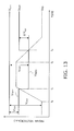
- FIG. 13 is a time chart illustrating an operation of the receiving circuit according to the second embodiment
- FIGS. 14A to 14E are time charts illustrating a simulation result of the receiving circuit according to the second embodiment
- FIG. 15 is a schematic view illustrating a receiving circuit according to a third embodiment
- FIGS. 16A to 17C are charts illustrating the characteristics of the receiving circuit according to a third embodiment
- FIG. 18 is a schematic view illustrating a receiving circuit according to a variation of the third embodiment.
- a receiving circuit includes a light receiving element, a signal voltage generation portion, a comparator, a reference voltage generation portion and a switch.
- the light receiving element receives a light signal and outputs a light current corresponding to the light signal.
- the signal voltage generation portion converts the light current into a signal voltage and outputs the signal voltage.
- the comparator compares the signal voltage with a first threshold value or a second threshold value.
- the reference voltage generation portion outputs a reference voltage input to the comparator.
- the switch changes the reference voltage to one of the first threshold value and the second threshold value based on an output of the comparator.
- FIG. 1 is a schematic view showing a receiving circuit 100 according to a first embodiment.
- the receiving circuit 100 is a receiving portion of a photo-coupler, for example.
- the receiving circuit 100 includes a photodiode 3 that is a light receiving element, a transimpedance amplifier (TIA) 7 , a differential amplifier 9 and a comparator 13 .
- TIA transimpedance amplifier
- the photodiode 3 is connected to the negative input of the TIA 7 .
- the photodiode 3 receives a light signal from a transmission portion (not illustrated) and outputs a light current I PD .
- the TIA 7 outputs a signal voltage V PD to a negative output terminal.
- the light current I PD is converted into the signal voltage V PD as indicated by formula (1).
- V PD ( R 3 +R 4) ⁇ I PD (1)
- a reference diode 5 is connected to the positive input of the TIA 7 , and a reference voltage V REF is output to a positive output terminal of the TIA 7 . It is preferable for the reference diode 5 to use a diode equivalent to the photodiode 3 .
- the photodiode 5 is provided on the same substrate as the photodiode 3 , being equal in size to the photodiode 3 , and having a shielded light receiving face.
- the term “equivalent” means that parameters for an equivalent circuit except a current source 25 corresponding to the light current I PD are the same between the photodiode 3 and the reference diode 5 .
- the term “same” includes not only a case where they are exactly equal but also a case where they are approximately the same, allowing small variations caused by circuit arrangement and processing accuracy.
- a circuit on the negative input side of the TIA 7 constitutes a signal voltage generation portion 10 , and converts the light current I PD into the signal voltage V PD and outputs it. Then, a circuit on the positive input side constitutes a reference voltage generation portion 20 , and outputs the reference voltage V REF .
- Feedback resistors R 3 and R 4 provided in the signal voltage generation portion 10 and feedback resistors R 1 , R 2 A and R 2 B provided in the reference voltage generation portion 20 satisfy a relationship in the following formula.
- R 1 +R 2 A+R 2 B R 3 +R 4 (2)
- the TIA 7 operates in all differential modes.
- the outputs V PD and V REF of the TIA 7 are amplified by the differential amplifier 9 , and are input to the comparator 13 .
- the reference voltage V REF is set to a threshold value, the level of the signal voltage V PD is determined and a high-level or low-level voltage is output. For example, when the V PD is higher than the V REF , a high-level voltage V H is output whereas, when the V PD is lower than the V REF , a low-level voltage V L is output.
- the output signal of the comparator 13 is processed by a DTC (dead time control) circuit 15 .
- the DTC circuit 15 Based on the output signal of the comparator 13 , the DTC circuit 15 outputs gate control signals to a PMOS transistor 21 and an NMOS transistor 23 , and the DTC circuit 15 also output a control signal to a switch control circuit 17 .
- the PMOS transistor 21 and the NMOS transistor 23 constitute an output stage that is configured with a CMOS inverter where the drain electrodes thereof are connected.
- the switch control circuit 17 outputs a control signal to an analogue switch 19 .
- the analogue switch 19 is connected in parallel to a feedback resistor R 2 B of the TIA 7 , and, while the analogue switch 19 is in on-state, it short-circuits the feedback resistor R 2 B. Thus, it is possible to switch the value of the feedback resistor of the TIA 7 and change the offset voltage V OS . That is, when the analogue switch 19 is turned on, the offset voltage V OS is changed from V OS1 to a voltage level V OS2 indicated by formula (4) below, and thus the level of the reference voltage V REF is changed.
- V OS2 R 2 A ⁇ I OS (4)
- the receiving circuit 100 changes the level of the reference voltage V REF based on the output of the comparator 13 .
- FIGS. 2A and 2B are time charts schematically showing the operation of the receiving circuit 100 .
- FIG. 2A shows the time variation of the signal voltage V PD and the reference voltage V REF .
- FIG. 2B shows the time variation of an output voltage V OUT .
- the reference voltage V REF is equal to the sum of the offset voltages V OS and V COM . Then, the reference voltage V REF is input to the comparator 13 as a first threshold value V REF1 or a second threshold value V REF2 for determining the level of the V PD .
- V REF1 V OS1 +V COM (5)
- V REF2 V OS2 +V COM (6)
- the V COM is equal to the output of the signal voltage generation portion 10 , while non light signal is input.
- the level of the signal voltage V PD starts to increase. Then, the output of the comparator 13 is inverted, when the V PD exceeds the first threshold value V REF1 at time t 1 , and, for example, the output voltage is shifted from the V H to the V L as shown in FIG. 2B .
- the switch control circuit 17 outputs a control signal, and the analogue switch 19 is turned on. Then, the reference voltage V REF is changed from the V REF1 to the V REF2 .
- the V PD is prevented from being lower than the second threshold value V REF2 . Hence, it is possible to stabilize the output of the comparator 13 and prevent malfunction.
- the V PD starts to decrease. Then, the output of the comparator 13 is inverted, when the V PD becomes lower than the second threshold value V REF2 at time t 3 , and the output voltage V OUT is shifted from V L to the V H . Simultaneously, the analogue switch 19 is turned off; the offset voltage V OS is returned from the V OS2 to the V OS1 ; and the threshold value is shifted from the V REF2 to the V REF1 .
- FIGS. 3A to 3D are time charts showing an example of the simulation results of the receiving circuit 100 .
- FIG. 3A shows variations in the light current I PD
- FIG. 3B shows variations in the signal voltage V PD and the reference voltage V REF
- FIG. 3C shows the V COMP of the comparator 13
- FIG. 3D shows the output voltage V OUT .
- a time period during which I PD rises is set relatively long so that the variations in the I PD easily cause chattering.
- the reference voltage V REF is either the first threshold value V REF1 or the second threshold value V REF2 .
- the signal voltage V PD exceeds the first threshold value V REF1 .
- the analogue switch 19 is turned on, and the reference voltage is decreased to the second threshold value V REF2 .
- the output V COMP of the comparator 13 is inverted from 0 V to 5 V, and the output voltage V OUT shown in FIG. 3D is shifted from 5 V to 0 V.
- FIGS. 4A to 4D are time charts showing the simulation results of the receiving circuit according to a comparative example.
- FIG. 4A shows variations in the light current I PD
- FIG. 4B shows variations in the signal voltage V PD and the reference voltage V REF .
- FIG. 4C shows variations in the output V COMP of the comparator 13
- FIG. 4D shows variations in the output voltage V OUT .
- the analogue switch 19 is not provided, and the offset voltage V OS is not varied. Therefore, as shown in FIG. 4B , the reference voltage V REF remains constant, i.e. the threshold value of the comparator 13 is not changed. For example, when the V PD exceeds the V REF at time t c shown in the figure, the output V COMP of the comparator 13 is inverted. Then, as shown in FIG. 4C , the variation in the V PD sometime causes chattering in which the output V COMP of the comparator 13 is repeatedly inverted. Then, as shown in FIG. 4D , chattering is caused also in the output voltage V OUT .
- FIGS. 5A to 5D are time charts showing other simulation results of the receiving circuit 100 .
- FIG. 5A shows variations in the light current I PD .
- FIG. 5B shows variations in the signal voltage V PD and the reference voltage V REF .
- FIGS. 5C and 5D respectively show the output V COMP of the comparator 13 and the output voltage V OUT .
- the photodiode 3 receives a light signal of a constant period, and outputs the light current I PD corresponding to the light signal.
- the signal voltage V PD is output from the signal voltage generation portion 10 as a pulse signal having constant rising time t r and falling time t f .
- the output of the comparator 13 is inverted. Since this simulation includes a transmission delay time T PLH as shown in FIG. 5C , the output V COMP of the comparator 13 is inverted with the delay time T PLH from a cross point between the V PD and the V REF1 in the rise. Then, the analogue switch 19 becomes on-state, and the reference voltage V REF is decreased to the second threshold value V REF2 .
- the signal voltage V PD decreases in a fall region. Then, when the signal voltage V PD becomes lower than the second threshold value V REF2 , the output of the comparator 13 is inverted from 5 V to 0 V. In this case, the inverse of the comparator is delayed by the transmission delay time T PHL . Simultaneously, the analogue switch 19 is turned off, and the reference voltage V REF is returned to the V REF1 .
- the output voltage V OUT shown in FIG. 5D is varied according to the output V COMP of the comparator 13 .
- V L the input (the turning on) of the light signal
- FIG. 6 is a schematic view illustrating the DTC circuit 15 .
- the DTC circuit 15 outputs gate control signals V PG and V NG , which are input to the gates of the PMOS transistor 21 and the NMOS transistor 23 in the output stage.
- the output V COMP of the comparator 13 is input to NAND gates 31 and 41 in the input stage of the DTC circuit 15 . Since the V COMP and the power V CC are input to the NAND gate 31 , when the V COMP is the V H , the V L is output whereas, when the V COMP is the V L , the V H is output.
- the output of the NAND gate 31 is input to the NAND gate 35 .
- the direct output of the NAND gate 31 and the output via an inverter 32 , a delay circuit 33 and an inverter 34 are input to the NAND gate 35 .
- the NAND gate 35 outputs a gate control signal V PG for the PMOS transistor 21 in the output stage.
- the gate control signal V PG is input via an inverter 36 to the gate of a CMOS invertor constituted by a PMOS transistor 37 and an NMOS transistor 39 , and its output is input to the gate of the PMOS transistor 21 .
- V COMP and the V PG inverted by the CMOS inverter are input to the NAND gate 41 .
- the output of the NAND gate 41 and the output of the NAND gate 31 via the delay circuit 33 are input to a NOR gate 43 .
- the NOR gate 43 outputs a gate control signal V NG for the NMOS transistor 23 in the output stage.
- the gate control signal V PG is input via an inverter 44 to the gate of a CMOS invertor constituted by a PMOS transistor 47 and an NMOS transistor 49 , and its output is input to the gate of the NMOS transistor 23 .
- FIGS. 7A to 7F are time charts illustrating the operation of the DTC circuit 15 .
- FIG. 7A shows the light current I PD
- FIG. 7B shows the signal voltage V PD and the reference voltage V REF .
- FIG. 7C shows the output V COMP of the comparator 13
- FIG. 7D shows the gate control signal V PG
- FIG. 7E shows the gate control signal V NG .
- FIG. 7F shows the output voltage V OUT .
- the signal voltage V PD corresponding to the light signal I o shown in FIG. 7A is output from the TIA 7 , and is compared by the comparator 13 with the reference voltage V REF which is a threshold value. Then, the V COMP shown in FIG. 7C is output from the comparator 13 .
- the output V COMP of the comparator 13 is input to the two NAND gates 31 and 41 in the input stage of the DTC circuit 15 . Then, the DTC circuit 15 outputs the gate control signal V PG shown in FIG. 7D and the gate control signal V NG shown in FIG. 7E .
- the gate control signal V PG is applied to the gate of the PMOS transistor 21 in the output stage, and the gate control signal V NG is applied to the gate of the NMOS transistor 23 .
- the output voltage V OUT shifts from the V H to the V L shown in FIG. 7F at the timing of the rise of the V NG , and shifts from the V L to the V H at the timing of the fall of the V PG .
- the gate control signal V PG shown in FIG. 7D is obtained by adding a delay portion (dead time) generated by the delay circuit 33 to the output waveform of the V COMP , increasing the pulse width of the V COMP .
- the gate control signal V NG shown in FIG. 7E is obtained by removing a portion corresponding to a delay time (dead time) of the delay circuit 33 , from a front portion of the output waveform of the V COMP , reducing the pulse width of the V COMP .
- the pulse width of the gate control signal V PG is formed so as to be larger backward and forward than the pulse width of the gate control signal V NG .
- the PMOS transistor 21 to which the gate control signal V PG is applied and the NMOS transistor 23 to which the gate control signal V NG is applied are prevented from being simultaneously turned on, and thus it is possible to prevent malfunction.
- FIG. 8 is a schematic view illustrating the switch control circuit 17 . As shown in the figure, the gate control signals V NG and V PG are also input from the DTC circuit 15 to the switch control circuit 17 .
- the switch control circuit 17 includes a DFF (delayed flip flop) 50 , outputs a switch control signal V ASC via its Q terminal, and controls the turning on and off of the analogue switch 19 .
- DFF delayed flip flop
- the output of a NOR gate 57 is supplied to the D terminal of the DFF 50 .
- the output voltage V OUT and the V L (0 V) are input to the NOR gate 57 .
- the V OUT is the V L
- the V H is output from the NOR gate 57
- the V L is output, when the V OUT is the V H .
- the power supply voltage V CC may be input to the NOR gate 57 .
- an AND gate 55 is supplied to a CLK terminal.
- the gate control signal V NG and the V NG via an inverter 51 , a delay circuit 52 and inverters 53 and 54 are input to the AND gate 55 .
- a pulse signal V NGE corresponding to the rise of the V NG is output from the AND gate 55 .
- an input level of the D terminal is held in the DFF 50 by the pulse signal V NGE input from the AND gate 55 , and a signal voltage V ASC is output from the Q terminal corresponding to the level held in the DFF 50 .
- an AND gate 65 is supplied to a CLR terminal.
- the gate control signal V PG inverted by an inverter 61 and the V PG via an inverter 62 , a delay circuit 63 and an inverter 64 are input to the AND gate 65 .
- a pulse signal V PGE corresponding to the fall of the V PG is output from the AND gate 65 .
- the input of the D terminal that has been held in the DFF 50 is cleared by the pulse signal V PGE input from the AND gate 65 , and the output of the Q terminal is also cleared.
- FIGS. 9A to 9F are time charts illustrating the operation of the switch control circuit 17 .
- FIG. 9A shows the gate control signal V NG
- FIG. 9B shows the pulse signal V NGE output from the AND gate 55 .
- FIG. 9C shows the gate control signal V PG
- FIG. 9D shows the pulse signal V PGE output from the AND gate 65 .
- FIG. 9E shows the switch control signal V ASC
- FIG. 9F shows variations in the reference voltage V REF and the signal voltage V PD .
- the AND gate 55 outputs the pulse signal V NGE corresponding to the rise of the gate control signal V NG .
- the AND gate 65 outputs the pulse signal V PGE corresponding to the fall of the gate control signal V PG .
- the switch control signal V ASC shown in FIG. 9E is output from the Q terminal of the DFF 50 . That is, the input of the D terminal is held in the DFF 50 by the pulse signal V NGE input to the CLK terminal.
- the V H is supplied to the D terminal.
- the output V ASC of the Q terminal is held at the V H (5 V).
- the pulse signal V PGE is input to the CLR terminal, the input V H of the D terminal is cleared, and the output V ASC of the Q terminal is shifted to the V L (0 V).
- FIG. 10 is a schematic view illustrating the analogue switch 19 .
- the analogue switch 19 is a CMOS switch that includes a PMOS transistor 77 and an NMOS transistor 79 connected in parallel.
- the switch control signal V ASC output from the switch control circuit 17 is applied to the gate of the NMOS transistor 79 via inverters 72 and 74 and a low-pass filter 71 .
- the V ASC inverted by an inverter 73 is applied to the gate of the PMOS transistor 77 via a low-pass filter 75 .
- the inverters 72 and 74 are provided so as to match the impedance on the side of the NMOS transistor 79 with the impedance of the PMOS transistor 77 .
- the analogue switch 19 is preferably configured so as not to feed switching noise to the feedback resistor R 2 B. For example, by inserting the low-pass filters 71 and 75 , the V ASC is gently shifted from the V L to the V H and from the V H to the V L . Thereby, it is possible to reduce differentiation noise that results in switching noise.
- FIG. 11 is a schematic view showing a receiving circuit 200 according to a variation of the first embodiment.
- the receiving circuit 200 differs from the receiving circuit 100 shown in FIG. 1 in that, in the feedback circuit of the signal voltage generation portion 10 , the same feedback resistors R 1 , R 2 A and R 2 B as the reference voltage generation portion 20 are provided, and that an analogue switch 19 b is connected between the resistors R 2 A and R 2 B.
- the analogue switch 19 b has the same configuration as an analogue switch 19 a that is connected in parallel to the feedback resistor R 2 B of the reference voltage generation portion 20 .
- the switch control signal V ASC output from the switch control circuit 17 the analogue switches 19 a and 19 b synchronize with each other and the turning on and off thereof is controlled.
- the analogue switch 19 b is a noise canceling circuit that generates switching noise equivalent to that of the analogue switch 19 a , and they cancel each other and thus it is possible to suppress the malfunction of the receiving circuit 200 .
- the analogue switch 19 is added to the feedback circuit of the TIA 7 included in the reference voltage generation portion 20 , and the reference voltage V REF is made to have hysteresis, and thus it is possible to suppress chattering.
- a monostable pulse signal is generated by the edge of the gate control signal V NG , and the DFF 50 may be set or reset receiving the monostable pulse signal.
- the gate of the CMOS inverter in the output stage may be driven by the output of the Q terminal of the DFF 50 .
- FIG. 12 is a schematic diagram showing a receiving circuit 300 according to a second embodiment. As shown in the figure, a photodiode 103 and a reference diode 105 equivalent to the photodiode 103 are provided in the input stage of the receiving circuit 300 .
- the photodiode 103 is connected to an input terminal on the negative side of a TIA 107 a (a first transimpedance amplifier) included in a signal voltage generation portion 110 .
- the reference diode 105 is connected to an input terminal on the negative side of a TIA 107 b (a second transimpedance amplifier) included in a reference voltage generation portion 120 .
- a common potential V COM is supplied to input terminals on the positive side of the TIA 107 a and the TIA 107 b.
- a signal voltage output from the TIA 107 a and the reference voltage V REF output from the TIA 107 b are input to a comparator 113 .
- Resistors R 6 A and R 6 B and a constant current source 108 a are provided between the output terminal of the TIA 107 a and an input terminal of the comparator 113 , and an offset voltage is added to the signal voltage V PD .
- resistors R 7 A and R 7 B and a constant current source 108 b are provided also between the output terminal of the TIA 107 b and the input terminal of the comparator 113 , and an offset voltage is added to the reference voltage V REF .
- the output of the comparator 113 is inverted by an inverter 121 , and is input to the DTC circuit 15 via a delay circuit 119 and inverters 122 and 123 .
- the DTC circuit 15 outputs, based on the output signal of the comparator 113 , the gate control signal to the PMOS transistor 21 and the NMOS transistor 23 in the output stage and the control signal to the switch control circuit 17 . Then, the switch control circuit 17 outputs the controls signals of analogue switches 90 a and 90 b.
- the receiving circuit 300 includes the analogue switch 90 b which switches the offset voltage on the side of the reference voltage V REF , based on the output of the comparator 113 , and the analogue switch 90 a which cancels the switching noise of the analogue switch 90 b.
- the analogue switch 90 a is a CMOS switch including an NMOS transistor 95 a and a PMOS transistor 97 a , and is on/off-controlled by the output of the switch control circuit 17 .
- the output of the switch control circuit 17 is inverted by an inverter 91 a , and is input to the gate of the NMOS transistor 95 a via an amplifier 93 a .
- the output of the switch control circuit 17 inverted by an inverter 91 is further inverted by an inverter 92 a , and is input to the gate of the PMOS transistor 97 a via an amplifier 94 a .
- the NMOS transistor 95 a and the PMOS transistor 97 a are turned on and off simultaneously.
- the analogue switch 90 b is a CMOS switch including an NMOS transistor 95 b and a PMOS transistor 97 b , and has the same configuration as the analogue switch 90 a . That is, the output of the switch control circuit 17 is input to the gate of the NMOS transistor 95 b via an inverter 91 b and an amplifier 93 b . The output of the switch control circuit 17 is input to the gate of the PMOS transistor 97 b via the inverters 91 b and 92 b and an amplifier 94 b.
- the analogue switch 90 b is connected in parallel to a resistor R 7 B provided on the side of the output of the TIA 107 b , and reduces the offset voltage while it is in on-state. Because of this, the reference voltage V REF is made to have hysteresis ⁇ V hys , and chattering is reduced.
- the analogue switch 90 a is connected between the resistors R 6 A and R 6 B on the side of the output of the TIA 107 a , whereby the switching noise of the analogue switch 90 b is cancelled by injecting noise having the same phase therewith.
- the value of the resistor R 6 B is set to be the same as the resistor R 7 B provided on the reference voltage V REF side.
- FIG. 13 is a time chart showing the operation of the receiving circuit 300 .
- the input V PD of the comparator 113 is expressed by formula (7) below.
- the reference voltage V REF is the first threshold value V REF1 given by formula (8) below, whereas the reference voltage V REF is the second threshold value V REF2 given by formula (9) below, while the analogue switch 90 b is in off-state.
- the output of the comparator is the high-level V H and the analogue switches 90 a and 90 b are in on-state.
- the reference voltage V REF is the first threshold value V REF1 .
- the signal voltage exceeds the first threshold value V REF1
- the output of the comparator 113 is inverted from the V H to the low-level V L .
- the analogue switches 90 a and 90 b are turned off, the reference voltage V REF is lowered to the second threshold value V REF2 .
- the analogue switch 90 b for switching the offset resistor is added to the side of the output of the TIA 107 b included in the reference voltage generation portion 120 , and thus the reference voltage V REF is made to have hysteresis ⁇ V hys , and thus it is possible to suppress chattering. Furthermore, by connecting the analogue switch 90 a to the side of the output of the signal voltage generation portion 110 , it is possible to cancel the switching noise of the analogue switch 90 b.
- FIGS. 14A to 14E are time charts showing the simulation result of the receiving circuit 300 .
- FIG. 14A shows the output V COMP of the comparator 113 .
- FIG. 14B shows the pulse signal V PGE output from the AND gate 65 in the switch control circuit 17
- FIG. 14C shows the pulse signal V NGE output from the AND gate 55 .
- FIG. 14D shows the variation of the reference voltage V REF and the signal voltage V PD .
- FIG. 14E shows the output V OUT of the receiving circuit 300 .
- the turning on and off of the analogue switches 90 a and 90 b is controlled by the pulse signal V PGE corresponding to the fall of the output V OUT of the comparator 113 and the pulse signal V NGE corresponding to the rise.
- the receiving circuit 300 is output the signal voltage V OUT having the same phase as the output V COMP of the comparator 113 .
- FIG. 15 is a schematic view showing a receiving circuit 400 according to a third embodiment.
- the receiving circuit 400 is, for example, a receiving portion of a photo-coupler, and detects the light emission of an LED 191 (light emitting diode) of a transmission portion 190 .
- the receiving circuit 400 includes the photodiode 3 , the reference diode 5 , the transimpedance amplifier (TIA) 7 , the differential amplifier 9 and the comparator 13 . Furthermore, in the embodiment, the receiving circuit 400 includes a switch circuit 150 for supplying the offset current I OS to a connecting point between the feedback resistors R 1 and R 2 in the TIA 7 .
- the photodiode 3 is connected to the negative input side of the TIA 7
- the reference diode 5 is connected to the positive input side of the TIA 7 .
- the reference diode 5 is equivalent to the photodiode 3 .
- the signal voltage generation portion 10 is provided on the negative input side of the TIA 7 , and includes feedback resistors R 3 and R 4 and a feedback capacitor C 2 .
- the signal voltage generation portion 10 converts the light current of the photodiode 3 into the signal voltage V PD and outputs it.
- the reference voltage generation portion 20 is provided on the positive input side of the TIA 7 , and includes the feedback resistors R 1 and R 2 and a feedback capacitor C 1 .
- the reference voltage generation portion 20 outputs the reference voltage V REF .
- the feedback resistors R 3 and R 4 provided in the signal voltage generation portion 10 and the feedback resistors R 1 and R 2 provided in the reference voltage generation portion 20 satisfy a relationship between formulas (10) and (11) below, and the TIA 7 operates in all differential modes.
- R 1 +R 2 R 3 +R 4 (10)
- C 1 C 2
- the outputs V PD and V REF of the TIA 7 are amplified by the differential amplifier 9 , and are input to the comparator 13 .
- the reference voltage V REF serves as a threshold value that determines the level of the signal voltage V PD and the comparator 13 outputs the voltage V H or V L depending on the level of V PD .
- the photodiode 3 is equivalent to the reference diode 5 . Therefore, when no light signal is input, the voltage levels of the outputs V PD and V REF of the TIA 7 are equal to each other. Accordingly, by supplying the offset current I OS between the feedback resistors R 1 and R 2 of the reference voltage generation portion 20 , the offset voltage V OS is added to the reference voltage V REF . Hence, a potential difference between the V PD and the V REF is produced, and the output of the comparator 13 is stabilized.
- the switch circuit 150 varies the offset current I OS and hysteresis is produced in the reference voltage V REF . Thereby, chattering is suppressed in the output voltage V OUT .
- the switch circuit 150 switches the offset current I OS by following variations in the output voltage V OUT .
- An output determination circuit 170 is provided between an output terminal 152 and the switch circuit 150 .
- the output determination circuit 170 includes an inverter 153 and an inverter 155 which are connected in series. Furthermore, a low-pass filter 180 may be provided between the inverter 153 and the inverter 155 .
- the switch circuit 150 includes an offset current source 141 that outputs an offset current I OS1 .
- a CMOS inverter including a PMOS transistor 125 and an NMOS transistor 127 is operated by the output voltage V OUT , and varies the offset current I OS .
- the NMOS transistor 125 when the voltage V H is input to the gate of the CMOS inverter, the NMOS transistor 125 is turned off, and the NMOS transistor 127 is turned on. Because of this, a current mirror circuit including an NMOS transistor 135 and an NMOS transistor 137 operates. When the current ratio between the NMOS transistor 135 and the NMOS transistor 137 is 1:1, the same current as the output I 2 of a constant current source 143 connected to the NMOS transistor 137 is added to the I OS .
- a current mirror circuit including a PMOS transistor 131 and a PMOS transistor 133 operates.
- the same current as the output I 1 of a constant current source 145 connected to the PMOS transistor 133 flows through the offset current source 141 , and thus the I OS becomes a current value obtained by subtracting the I 1 from the I OS1 .
- the offset current I OS is I OS1 +I 2
- the offset current I OS is I OS1 ⁇ I 1
- the V OUT is the V L .
- the output of the comparator 13 is inverted by an inverter 151 and is output to the output terminal 152 as V OUT . Therefore, when the signal voltage V PD is varied from the low level (L) to the high level (H) at the input side of the comparator 13 , the reference voltage V REF is varied from the V REF1 to the V REF2 , and the hysteresis ⁇ V hys is produced as expressed by formula (14) below.
- ⁇ V hys R 2 ⁇ ( I 1 +I 2 ) (14)
- M is the conversion ratio in the light connection, that is, the ratio between the drive current I F of the LED 191 and the light current of the photodiode 3 .
- I Fhys M ⁇ [R 2/( R 1 +R 2)] ⁇ ( I 1 +I 2 ) (17)
- FIGS. 16A to 17C are charts showing the simulation results of the characteristics of the receiving circuit 400 .
- FIGS. 16A to 16C show the outputs V REF and V PD of the TIA 7 and the output voltage V OUT when the drive current I F of the LED 191 is varied from L to H.
- the horizontal axis is the input voltage V IN of the transmission portion 190 .
- FIGS. 17A to 17C show the individual characteristics, when the drive current I F of the LED 191 is varied from H to L.
- the input voltage V IN is varied from the L level to the H level. Accordingly, the drive current I F of the transmission portion 190 is increased.
- the V PD is also increased and intersects with the reference value V REF1 at a cross point 1 (CP 1 ).
- the drive current I FH of the LED 191 corresponding to the CP 1 is 1 mA, and an input voltage at that time is about 1.75 V.
- the output of the comparator 13 is inverted from L to H, and the output voltage V OUT is inverted from H to L. Then, the offset current I OS is varied from I OS1 +I 2 to I OS1 ⁇ I 1 , and the offset voltage V OS is decreased. Thereby, the reference voltage V REF is decreased to the V REF2 , and the hysteresis ⁇ V hys is produced.
- the input voltage V IN is varied from the H level to the L level. Accordingly, the drive current I F of the LED 191 is reduced.
- the V PD is decreased and intersects with the reference voltage V REF2 at a cross point (CP 2 ).
- the drive current I FL of the LED 191 corresponding to the CP 2 is 0.8 mA, and the input voltage at that time is about 1.62 V.
- the hysteresis I Fhys of the drive current I FL is about 0.2 mA, and the voltage at the cross point is decreased by about 0.13 V.
- the output of the comparator 13 is inverted from H to L, and the output voltage V OUT is inverted from L to H. Then, the offset current I OS is varied from I OS1 ⁇ I 1 to I OS1 +I 2 , and the reference voltage V REF is increased to the V REF1 .
- the receiving circuit 500 includes the photodiode 3 , the reference diode 5 , the transimpedance amplifier (TIA) 7 , the differential amplifier 9 and the comparator 13 . Furthermore, the receiving circuit 500 includes a switch circuit 160 for supplying the offset current I OS between the feedback resistors R 1 and R 2 in the TIA 7 .
- the photodiode 3 is connected to the negative input side of the TIA 7
- the reference diode 5 is connected to the positive input side of the TIA 7 .
- the reference diode 5 is equivalent to the photodiode 3 .
- the signal voltage generation portion 10 is configured on the negative input side of the TIA 7 , and includes the feedback resistors R 3 and R 4 and the feedback capacitor C 2 .
- the signal voltage generation portion 10 converts the light current of the photodiode 3 into the signal voltage V PD and outputs it.
- the reference voltage generation portion 20 is configured on the positive input side of the TIA 7 , and includes the feedback resistors R 1 and R 2 and the feedback capacitor C 1 .
- the reference voltage generation portion 20 outputs the reference voltage V REF .
- the feedback resistors R 3 and R 4 provided in the signal voltage generation portion 10 and the feedback resistors R 1 and R 2 provided in the reference voltage generation portion 20 satisfy a relationship between formulas (10) and (11), and the TIA 7 operates in all differential modes.
- the outputs V PD and V REF of the TIA 7 are amplified by the differential amplifier 9 , and are input to the comparator 13 .
- the reference voltage V REF serves as a threshold value that determine the level of the signal voltage V PD and the comparator outputs the voltage V H or V L depending on the level of V PD .
- the output voltage V OUT inverted by the inverter 151 is fed back through the switch circuit 160 , thus switching the offset current I OS .
- the output determination circuit 170 is provided between the output terminal V OUT and the switch circuit 160 .
- the output determination circuit 170 includes the inverter 153 and the inverter 155 which are connected in series.
- the low-pass filter 180 may be provided between the inverter 153 and the inverter 155 .
- the output voltage V OUT is inverted by an inverter 157 , and is input to the switch circuit 160 .
- the switch circuit 160 includes the offset current source 141 that outputs the offset current I OS1 .
- a PMOS transistor 165 is operated by the output voltage V OUT and varies the offset current I OS .
- the PMOS transistor 165 when the voltage V H is input to the gate of the PMOS transistor 165 , the PMOS transistor 165 is turned off, and the gate voltage of PMOS transistors 161 and 163 is decreased, turning on the PMOS transistors 161 and 163 .
- a current mirror circuit including the PMOS transistor 161 and a PMOS transistor 163 is operated. If the current ratio between the PMOS transistor 161 and the PMOS transistor 163 is 1:1, the same current as the output I 1 of a constant current source 145 connected to the PMOS transistor 163 flows through the offset current source 141 . Because of this, the offset voltage V OS is decreased to I OS1 ⁇ I 1 , and the reference voltage V REF is lowered.
- the output voltage of the comparator 13 is inverted by the inverter 151 and the inverted voltage thereof is output to the output terminal 152 as V OUT . Then, the V OUT is input to the gate of the PMOS transistor 165 via the output determination circuit 170 that inverts an input voltage. As a result, the voltage level input to the gate of the PMOS transistor 165 is the same with the output voltage of the comparator 13 . That is, when the V H is input to the gate of the PMOS transistor 165 , the output voltage of the comparator 13 is V H and the reference voltage V REF is lowered.
- the voltage V L is input to the gate of the PMOS transistor 165 .
- the PMOS transistor 165 is turned on, and the gate voltage of the PMOS transistors 161 and 163 is increased, turning off the PMOS transistors 161 and 163 .
- the offset current is increased to I OS1 , and the reference voltage V REF is increased.
- hysteresis is produced in the reference voltage V REF , and thus it is possible to suppress chattering in the output voltage V OUT .
- the switch circuits 150 and 160 switch the offset current I OS added to the reference voltage generation portion 20 , and thus the offset voltage V OS is varied and hysteresis is produced in the reference voltage V REF . Because of this, malfunction in the output voltage V OUT is suppressed.
Landscapes
- Physics & Mathematics (AREA)
- General Physics & Mathematics (AREA)
- Spectroscopy & Molecular Physics (AREA)
- Nonlinear Science (AREA)
- Amplifiers (AREA)
- Light Receiving Elements (AREA)
Abstract
Description
V PD=(R3+R4)×I PD (1)
R1+R2A+R2B=R3+R4 (2)
V OS2 =R2A×I OS (4)
V REF1 =V OS1 +V COM (5)
V REF2 =V OS2 +V COM (6)
R1+R2=R3+R4 (10)
C1=C2
V REF1 =R2×(I OS1 +I 2)(V OUT =V H) (12)
V REF2 =R2×(I OS1 −I 1)(V OUT =V L) (13)
ΔV hys =R2×(I 1 +I 2) (14)
I FH =M×[R2/(R1+R2)]×(I OS1 +I 2) (15)
I FL =M×[R2/(R1+R2)]×(I OS1 −I 1) (16)
I Fhys =M×[R2/(R1+R2)]×(I 1 +I 2) (17)
Claims (20)
Applications Claiming Priority (2)
| Application Number | Priority Date | Filing Date | Title |
|---|---|---|---|
| JP2011087208A JP5514142B2 (en) | 2011-04-11 | 2011-04-11 | Receiver circuit |
| JP2011-087208 | 2011-04-11 |
Publications (2)
| Publication Number | Publication Date |
|---|---|
| US20120256081A1 US20120256081A1 (en) | 2012-10-11 |
| US8803116B2 true US8803116B2 (en) | 2014-08-12 |
Family
ID=46965349
Family Applications (1)
| Application Number | Title | Priority Date | Filing Date |
|---|---|---|---|
| US13/412,462 Active 2033-02-02 US8803116B2 (en) | 2011-04-11 | 2012-03-05 | Receiving circuit having a switch for changing the generated reference voltage to one of a first and a second threshold value |
Country Status (3)
| Country | Link |
|---|---|
| US (1) | US8803116B2 (en) |
| JP (1) | JP5514142B2 (en) |
| CN (1) | CN102739233B (en) |
Families Citing this family (9)
| Publication number | Priority date | Publication date | Assignee | Title |
|---|---|---|---|---|
| US9847842B2 (en) * | 2014-03-03 | 2017-12-19 | Panasonic Intellectual Property Management Co., Ltd. | Optical reception circuit |
| JP6426406B2 (en) * | 2014-08-29 | 2018-11-21 | 株式会社東芝 | Optical receiver circuit and optical coupler |
| US9553540B2 (en) * | 2015-01-21 | 2017-01-24 | Ford Global Technologies, Llc | Power converter with pre-compensation for dead-time insertion |
| US10270364B2 (en) * | 2015-01-21 | 2019-04-23 | Ford Global Technologies, Llc | Power converter with dead-time variation to disperse distortion |
| CN106330340B (en) * | 2016-09-23 | 2019-07-26 | 深圳市英特源电子有限公司 | Optical receiving circuit and the method for preventing logic exception |
| CN106953629A (en) * | 2017-04-11 | 2017-07-14 | 深圳飞沃拜特技术有限公司 | Isolated digital input circuit |
| CN110967683B (en) * | 2019-12-12 | 2022-04-01 | 上海禾赛科技有限公司 | Signal receiving and amplifying circuit and laser radar with same |
| EP4254802A4 (en) * | 2020-12-28 | 2024-01-17 | Suteng Innovation Technology Co., Ltd | Laser receiving circuit and laser radar |
| US12298181B2 (en) * | 2023-09-06 | 2025-05-13 | Apple Inc. | Systems and methods for crosstalk mitigation between ambient light sensor and electronic display |
Citations (5)
| Publication number | Priority date | Publication date | Assignee | Title |
|---|---|---|---|---|
| JPH03179816A (en) | 1989-09-14 | 1991-08-05 | Omron Corp | Electronic switch |
| US5319265A (en) | 1991-10-25 | 1994-06-07 | Samsung Electronics Co., Ltd. | Comparator with hysteresis |
| JP2003008408A (en) | 2001-06-20 | 2003-01-10 | Olympus Optical Co Ltd | Hysteresis comparator circuit |
| JP2007109944A (en) | 2005-10-14 | 2007-04-26 | Toshiba Corp | Receiver |
| US7868701B2 (en) * | 2004-08-03 | 2011-01-11 | Nippon Telephone And Telegraph Corporation | Transimpedance amplifier |
Family Cites Families (9)
| Publication number | Priority date | Publication date | Assignee | Title |
|---|---|---|---|---|
| JPS5454281A (en) * | 1977-10-08 | 1979-04-28 | Sunx Ltd | Device for providing photoelectric switch with hysteresis characteristic |
| JPS586480A (en) * | 1981-07-03 | 1983-01-14 | Ricoh Co Ltd | Reflection detection device |
| JPH02157666A (en) * | 1988-12-09 | 1990-06-18 | Matsushita Electric Ind Co Ltd | signal comparator |
| JPH08154047A (en) * | 1994-11-25 | 1996-06-11 | Sunx Ltd | Detection switch |
| JP3516556B2 (en) * | 1996-08-02 | 2004-04-05 | 沖電気工業株式会社 | Internal power supply circuit |
| JP2002250659A (en) * | 2001-02-23 | 2002-09-06 | Matsushita Electric Works Ltd | Illuminance sensor |
| JP3947044B2 (en) * | 2002-05-31 | 2007-07-18 | 富士通株式会社 | Input/Output Buffers |
| JP4927664B2 (en) * | 2007-08-14 | 2012-05-09 | 日本電信電話株式会社 | Preamplifier circuit |
| JP2011035867A (en) * | 2009-08-06 | 2011-02-17 | Renesas Electronics Corp | Amplifier circuit and light receiving amplifier circuit employing the same |
-
2011
- 2011-04-11 JP JP2011087208A patent/JP5514142B2/en active Active
-
2012
- 2012-03-05 US US13/412,462 patent/US8803116B2/en active Active
- 2012-03-16 CN CN201210070740.3A patent/CN102739233B/en active Active
Patent Citations (6)
| Publication number | Priority date | Publication date | Assignee | Title |
|---|---|---|---|---|
| JPH03179816A (en) | 1989-09-14 | 1991-08-05 | Omron Corp | Electronic switch |
| US5319265A (en) | 1991-10-25 | 1994-06-07 | Samsung Electronics Co., Ltd. | Comparator with hysteresis |
| JP2003008408A (en) | 2001-06-20 | 2003-01-10 | Olympus Optical Co Ltd | Hysteresis comparator circuit |
| US7868701B2 (en) * | 2004-08-03 | 2011-01-11 | Nippon Telephone And Telegraph Corporation | Transimpedance amplifier |
| JP2007109944A (en) | 2005-10-14 | 2007-04-26 | Toshiba Corp | Receiver |
| US20070126507A1 (en) | 2005-10-14 | 2007-06-07 | Kabushiki Kaisha Toshiba | Receiving apparatus |
Non-Patent Citations (1)
| Title |
|---|
| Japanese Office Action dated Dec. 16, 2013, filed in Japanese counterpart Application No. 2011-087208, 4 pages (with translation). |
Also Published As
| Publication number | Publication date |
|---|---|
| CN102739233A (en) | 2012-10-17 |
| US20120256081A1 (en) | 2012-10-11 |
| CN102739233B (en) | 2015-08-05 |
| JP5514142B2 (en) | 2014-06-04 |
| JP2012222640A (en) | 2012-11-12 |
Similar Documents
| Publication | Publication Date | Title |
|---|---|---|
| US8803116B2 (en) | Receiving circuit having a switch for changing the generated reference voltage to one of a first and a second threshold value | |
| US10003265B2 (en) | Switching power supply device | |
| US9350341B2 (en) | Gate driver, switch control circuit and power supply device comprising the gate driver circuit | |
| US7813392B2 (en) | Light transmitter and automatic power control circuit thereof | |
| JP5148537B2 (en) | Power supply voltage detection circuit | |
| JP4184391B2 (en) | Comparison circuit and infrared receiver | |
| US8102217B2 (en) | Oscillator having feedback path which is capable of supplying reduced voltage potential to oscillation circuit | |
| JP4119784B2 (en) | Power-on reset circuit | |
| US9031108B2 (en) | Circuitry and method for driving laser with temperature compensation | |
| KR20090034762A (en) | Semiconductor circuit | |
| TWI530071B (en) | DC/DC converter | |
| US10666250B2 (en) | Drive device for semiconductor element | |
| JP2011259036A (en) | Comparator circuit | |
| JP4731257B2 (en) | Abnormal connection detection circuit and drive device provided with abnormal connection detection circuit | |
| US20120176040A1 (en) | Indicator drive circuit | |
| KR100859780B1 (en) | Current to voltage converter and current to voltage conversion method | |
| JP6914010B2 (en) | Drive device | |
| JP2020202695A (en) | Switching power supply device | |
| JP2005210558A (en) | Optical current/voltage conversion circuit | |
| JP7129366B2 (en) | switching power supply | |
| US9332600B2 (en) | Driving circuit for light emitting element, and light emitting device | |
| JP2013098471A (en) | Optically-coupled insulating circuit | |
| JP2021027549A (en) | Semiconductor amplifier circuit | |
| JP2006186344A (en) | Optical coupling device | |
| JP7542455B2 (en) | Switching Power Supply Unit |
Legal Events
| Date | Code | Title | Description |
|---|---|---|---|
| AS | Assignment |
Owner name: KABUSHIKI KAISHA TOSHIBA, JAPAN Free format text: ASSIGNMENT OF ASSIGNORS INTEREST;ASSIGNOR:TSUNETSUGU, YUKIO;REEL/FRAME:027808/0266 Effective date: 20120217 |
|
| STCF | Information on status: patent grant |
Free format text: PATENTED CASE |
|
| FEPP | Fee payment procedure |
Free format text: PAYER NUMBER DE-ASSIGNED (ORIGINAL EVENT CODE: RMPN); ENTITY STATUS OF PATENT OWNER: LARGE ENTITY Free format text: PAYOR NUMBER ASSIGNED (ORIGINAL EVENT CODE: ASPN); ENTITY STATUS OF PATENT OWNER: LARGE ENTITY |
|
| MAFP | Maintenance fee payment |
Free format text: PAYMENT OF MAINTENANCE FEE, 4TH YEAR, LARGE ENTITY (ORIGINAL EVENT CODE: M1551) Year of fee payment: 4 |
|
| MAFP | Maintenance fee payment |
Free format text: PAYMENT OF MAINTENANCE FEE, 8TH YEAR, LARGE ENTITY (ORIGINAL EVENT CODE: M1552); ENTITY STATUS OF PATENT OWNER: LARGE ENTITY Year of fee payment: 8 |
|
| MAFP | Maintenance fee payment |
Free format text: PAYMENT OF MAINTENANCE FEE, 12TH YEAR, LARGE ENTITY (ORIGINAL EVENT CODE: M1553); ENTITY STATUS OF PATENT OWNER: LARGE ENTITY Year of fee payment: 12 |