US8780273B2 - Signal processing apparatus, signal processing method, and program - Google Patents
Signal processing apparatus, signal processing method, and program Download PDFInfo
- Publication number
- US8780273B2 US8780273B2 US13/210,629 US201113210629A US8780273B2 US 8780273 B2 US8780273 B2 US 8780273B2 US 201113210629 A US201113210629 A US 201113210629A US 8780273 B2 US8780273 B2 US 8780273B2
- Authority
- US
- United States
- Prior art keywords
- output
- input
- signal
- color difference
- luminance signal
- Prior art date
- Legal status (The legal status is an assumption and is not a legal conclusion. Google has not performed a legal analysis and makes no representation as to the accuracy of the status listed.)
- Expired - Fee Related, expires
Links
Images


Classifications
-
- H—ELECTRICITY
- H04—ELECTRIC COMMUNICATION TECHNIQUE
- H04N—PICTORIAL COMMUNICATION, e.g. TELEVISION
- H04N9/00—Details of colour television systems
- H04N9/77—Circuits for processing the brightness signal and the chrominance signal relative to each other, e.g. adjusting the phase of the brightness signal relative to the colour signal, correcting differential gain or differential phase
Definitions
- the present disclosure relates to a signal processing apparatus, a signal processing method, and a program.
- JP-A Japanese Patent Application Laid-Open
- a characteristic curve expressed as a free curve may be used so as to emphasize a black color in an image. If the color signals are corrected, a relatively high processing load is necessary, but an image having an emphasized black color can be appropriately displayed. However, if only a luminance signal is corrected, a processing load is reduced, but an image may deteriorate, for example, a flesh color in an image may look reddish.
- a signal processing apparatus including a gamma correction circuit that performs gamma correction on an input luminance signal and generates an output luminance signal, an output-to-input ratio calculation circuit that calculates a ratio of the output luminance signal to the input luminance signal as an output-to-input ratio of a luminance signal, and a color difference correction circuit that multiplies an input color difference signal by the output-to-input ratio of the luminance signal and generates an output color difference signal.
- the color difference correction circuit may revise the output-to-input ratio of the luminance signal in response to the input color difference signal, multiplies the input color difference signal by the revised output-to-input ratio of the luminance signal, and generates the output color difference signal.
- the output-to-input ratio of the luminance signal may be revised so that influence of color difference correction increases as an absolute value of a color difference value represented by the input color difference signal decreases.
- the output-to-input ratio calculation circuit may calculate the output-to-input ratio of the luminance signal, without performing a division operation, using a calculation table specifying a relationship between an input value of the luminance signal and a ratio of an output value to the input value of the luminance signal.
- the gamma correction circuit may calculate an output value of the luminance signal, without performing a division operation, using a calculation table specifying a relationship between an input value of the luminance signal and a ratio of the output value of the luminance signal.
- a signal processing method including performing gamma correction on an input luminance signal and generating an output luminance signal, calculating a ratio of the output luminance signal to the input luminance signal as an output-to-input ratio of a luminance signal, and multiplying an input color difference signal by the output-to-input ratio of the luminance signal and generating an output color difference signal.
- a program causing a computer to execute the signal processing method.
- the program may be provided using a computer readable recording medium or may be provided through a communication means.
- a signal processing apparatus a signal processing method, and a program which are capable of suppressing deterioration of a gamma-corrected image can be provided.
- FIG. 1 is a block diagram illustrating a main configuration of a signal processing apparatus according to an embodiment of the present disclosure.
- FIG. 2 is a flowchart illustrating an operation procedure of a signal processing apparatus.
- FIG. 3 is a block diagram illustrating a configuration of a gamma correction circuit.
- FIG. 4 is a view illustrating an example of a characteristic curve for gamma correction.
- FIG. 5 is a view illustrating a method of calculating an output-to-input ratio.
- FIG. 6 is a view illustrating a method of revising an output-to-input ratio (1 ⁇ 2).
- FIG. 7 is a view illustrating a method of revising an output-to-input ratio ( 2/2).
- FIG. 8 is a view illustrating an example of a signal processing result.
- FIG. 1 illustrates the main configuration of the signal processing apparatus 1 .
- the signal processing apparatus 1 is applied to an apparatus, which performs gamma correction on an image signal or a video signal, such as a display device, an image recording/reproducing apparatus, and a video recording/reproducing apparatus.
- an apparatus that performs gamma correction on a video signal S will be described as an example.
- the signal processing apparatus 1 includes an input terminal 11 , a separation circuit 12 , a gamma correction circuit 13 , an output-to-input ratio calculation circuit 14 , a color difference correction circuit 15 , and an RGB conversion circuit 16 .
- the input terminal 11 supplies the separation circuit 12 with the input video signal S.
- the separation circuit 12 supplies the gamma correction circuit 13 and the output-to-input ratio calculation circuit 14 with the input luminance signal Y and supplies the color difference correction circuit 15 with the input color difference signals Cb and Cr.
- the gamma correction circuit 13 performs gamma correction on the input luminance signal Y supplied from the separation circuit 12 using a characteristic curve for gamma correction.
- the gamma correction circuit 13 supplies the output-to-input ratio calculation circuit 14 and the RGB conversion circuit 16 with a gamma-corrected output luminance signal Y′.
- the output-to-input ratio calculation circuit 14 supplies the color difference correction circuit 15 with the calculation result.
- the color difference correction circuit 15 multiplies the input color difference signals Cb and Cr supplied from the separation circuit 12 by the output-to-input ratio p and corrects the input color difference signals Cb and Cr.
- the color difference correction circuit 15 supplies the RGB conversion circuit 16 with output color difference signals Cb′ and Cr′ obtained by color difference correction.
- the RGB conversion circuit 16 receives the output luminance signal Y′ and the output color difference signals Cb′ and Cr′ and converts the output luminance signal Y′ and the output color difference signals Cb′ and Cr′ into color signals R, G, and B.
- the RGB conversion circuit 16 outputs the color signals R, G, and B to a display device (not shown) or a subsequent processing apparatus.
- the input luminance signal Y and the input color difference signals Cb and Cr may be separately input.
- the separation circuit 12 may be omitted.
- the output luminance signal Y′ and the output color difference signals Cb′ and Cr′ may be separately output.
- the RGB conversion circuit 16 may be omitted.
- FIG. 2 illustrates the operation procedure of the signal processing apparatus 1 .
- the separation circuit 12 first separates the video signal S into the input luminance signal Y and the input color difference signals Cb and Cr (step S 11 ).
- the RGB conversion circuit 16 converts the output luminance signal Y′ and the output color difference signals Cb′ and Cr′ into the color signals R, G, and B and outputs the color signals R, G, and B for the sake of a subsequent device or subsequent processing (step S 15 ).
- FIG. 3 illustrates the configuration of the gamma correction circuit 13
- FIG. 4 illustrates an example of a characteristic curve for gamma correction.
- the gamma correction circuit 13 includes a comparator 21 , a coefficient calculation circuit 22 , various calculators 23 , 25 , and 27 , flip flops 24 , 26 , and 29 , and an overflow limiter 28 .
- a characteristic curve represents a relationship between an input value x (a horizontal axis) and an output value b (a vertical axis) of the luminance signal through a free curve. Both the input value x and the output value b of the luminance signal are represented by a value ranging from 0 to 225.
- the characteristic curve is divided into a predetermined number of sections, and an input-output relationship in each section is linearly approximated.
- the characteristic curve is divided into 12 sections.
- the input value x is divided into sections of 0 to x1, x1 to x2, . . . , and x11 to 255
- the output value b is divided into sections of 0 to b1, b1 to b2, . . . , and b11 to 255 that correspond to the sections of the input value x.
- Each section of the input value x may be divided at an arbitrary width or a constant width.
- the input luminance signal Y from the separation circuit 12 is supplied to the gamma correction circuit 13 .
- the input luminance signal Y is supplied to the subtractor 23 and the comparator 21 .
- a value of the input luminance signal Y (also referred to as an “input luminance value Y”) is compared with the sections of the characteristic curve, and the section to which the input luminance value Y belongs is specified.
- a specifying result of the section is supplied to the coefficient calculation circuit 22 .
- the minimum input value xmin is supplied to the subtractor 23 , the gradient a of the approximate curve is supplied to the multiplier 25 , and the minimum output value bmin is supplied to the adder 27 .
- the minimum input value xmin and the minimum output value bmin of each section and the gradient a of the approximate curve in each section are recorded in a memory (not shown) in the form of a table as coefficient calculation data.
- the output luminance signal Y′ obtained by performing gamma correction on the input luminance signal Y is generated using the characteristic curve specifying the input-output relationship of the luminance value Y.
- the output luminance signal Y′ is “a5 ⁇ (Y ⁇ x5)+b5”
- the output luminance signal Y′ can be calculated without performing a division operation.
- a table for storing an enormous amount of reciprocal value data used for a division operation can be omitted, so that the circuit size can be reduced.
- FIG. 5 illustrates a method of calculating the output-to-input p.
- a horizontal axis represents the input value x of the section to which the input luminance value Y belongs (see FIG. 4 ), and a vertical axis represents the output-to-input ratio p corresponding to the input value x of the horizontal axis.
- the output-to-input ratio p corresponding to the input luminance signal Y is “(b6/x6 ⁇ b5/x5) ⁇ (Y ⁇ x5)+b5/x5.”
- the output-to-input ratio p can be calculated without performing a division operation.
- a table for storing an enormous amount of reciprocal value data used for a division operation can be omitted, so that the circuit size can be reduced.
- the operation of the color difference correction circuit 15 will be described.
- the input color difference signals Cb and Cr supplied from the separation circuit 12 are multiplied by the output-to-input ratio p supplied from the output-to-input ratio calculation circuit 14 , so that the output color difference signals Cb′ and Cr′ are generated.
- the output color difference signals Cb′ and Cr′ in which color difference correction has been performed in view of influence of gamma correction can be obtained.
- deterioration of an image can be further suppressed.
- the output color difference signals Cb′ and Cr′ may be generated by multiplying the input color difference signals Cb and Cr by an output-to-input ratio p′ that is revised according to the values of the input color difference signals Cb and Cr.
- the revised output-to-input ratio p′ is used in color difference correction but not used in gamma correction.
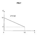
- FIGS. 6 and 7 illustrate a method of revising the output-to-input ratio p.
- FIG. 6 illustrates a relationship between an input value Cmax of a color difference signal and a revision coefficient k for revising the output-to-input ratio p.
- the color difference is represented as a positive value or a negative value through a value, which ranges from ⁇ 128 to +127, obtained by subtracting 128 from the input values Cb and Cr.
- the revision coefficient k is set to increase as the absolute value Cmax of the color difference decreases.
- the revision coefficient k is 1.0 when the absolute value Cmax of the color difference is zero (0) and is 0.0 when the absolute value Cmax of the color difference is 128 (or 127).
- ka is a gradient of a straight line in FIG. 6
- Cmax is “max(
- FIG. 7 illustrates a relationship between the revision coefficient k and the revised output-to-input ratio p′.
- a horizontal axis represents the revision coefficient k (0.0 ⁇ k ⁇ 1.0) obtained according to FIG. 6
- a vertical axis represents the output-to-input ratio p′ (p ⁇ p′ ⁇ 1.0) revised by the revision coefficient k.
- the revised output-to-input ratio p′ is p when the absolute value Cmax of the color difference is zero (0) and is 1 when the absolute value Cmax of the color difference is 128 (or 127).
- An upper limit value or a lower limit value of the revision coefficient k may be adjusted so as to adjust influence of color difference correction. That is, in order to decrease influence of color difference correction, the upper limit value may be set to be small, and in order to increase influence of color difference correction, the lower limit value may be set to be large.
- the relationship between the input values Cb and Cr of the color difference signal and the revision coefficient k (the relationship illustrated in FIG. 6 ) may be defined by any other straight line or curve. Further, the relationship between the revision coefficient k and the revised output-to-input ratio p′ (the relationship illustrated in FIG. 7 ) may be defined by any other relationship equation.
- FIG. 8 illustrates an example of a signal processing result by the signal processing apparatus 1 .
- a value of a signal processing result is represented with values after the decimal point omitted.
- [19, 143, 150] is generated from the first input signal S 1 as a first output signal S 1 ′ [Y′, Cb′, Cr′], and [140, 144, 151] is generated from the second input signal S 2 as a second output signal S 2 ′ [Y′, Cb′, Cr′].
- the input signal [Y, Cb, Cr] is normalized, and the normalized input signal is converted into the color signal using a conversion equation that conforms to ITU-R BT. 709 Recommendation (Rec. 709).
- the converted color signal is subjected to gamma correction, and the gamma-corrected color signal is converted into the output signal [Y′, Cb′, Cr′].
- [19, 150, 160] is generated from the first input signal S 1 as the first output signal S 1 ′ [Y′, Cb′, Cr′], and [140, 150, 160] is generated from the second input signal S 2 as the second output signal S 2 ′ [Y′, Cb′, Cr′].
- the color signal is not converted, and gamma correction is performed only on the luminance signal using the characteristic curve for gamma correction similar to the first method.
- color difference correction is further performed on the color signals Cb and Cr using the output-to-input ratio p of the luminance signal.
- the luminance value Y of the first output signal S 1 ′ is corrected from [32] to [19] in any of the methods.
- the color difference values Cb and Cr of the first output signals S 1 ′ are corrected from [150, 160] to [143, 150] in the first method, not corrected in the second method, and corrected to [141, 147] in the third method.
- the luminance value Y of the second output signal S 2 ′ is corrected from [200] to [140] in any of the methods.
- the color difference values Cb and Cr of the second output signals S 2 ′ are corrected from [150, 160] to [144, 151] in the first method, not corrected in the second method, and corrected to [143, 150] in the third method.
- the color difference values have been corrected to the color difference values Cb′ and Cr′ closer to when gamma correction is performed on the color signal (the first method) than when gamma correction is performed only on the luminance signal (the second method).
- the signal processing apparatus 1 and the signal processing method according to the embodiments of the present disclosure by correcting the input color difference signals Cb and Cr using the output-to-input ratio p (or the revised output-to-input ratio p′) of the luminance signal, the output color difference signals Cb′ and Cr′ in which color difference correction has been performed in view of influence of gamma correction can be generated.
- the output color difference signals Cb′ and Cr′ in which color difference correction has been performed in view of influence of gamma correction can be generated.
- deterioration of an image can be further suppressed.
- the above description has been made in connection with the case of implementing the signal processing method according to the present disclosure using the hardware configuration including the gamma correction circuit 13 , the output-to-input ratio calculation circuit 14 , and the color difference correction circuit 15 .
- the signal processing method according to the present disclosure may be implemented using a software configuration instead of the hardware configuration.
- the signal processing method may be implemented by a program executed on a processor such as a central processing unit (CPU) or a digital signal processor (DSP).
- CPU central processing unit
- DSP digital signal processor
Abstract
Description
Y′=a·(Y−xmin)+bmin (1)
p=α(Y−xa)+pa (2),
where α=(pb−pa)/(xb−xa)
Cb′=p·Cb
Cr′=p·Cr (3)
k=ka·Cmax+kb, (4)
p′=1−(1−p)·k (5)
Cb′=p′·Cb
Cr′=p′·Cr (6)
Claims (8)
Applications Claiming Priority (2)
| Application Number | Priority Date | Filing Date | Title |
|---|---|---|---|
| JPP2010-187372 | 2010-08-24 | ||
| JP2010187372A JP2012049627A (en) | 2010-08-24 | 2010-08-24 | Signal processing apparatus, signal processing method and program |
Publications (2)
| Publication Number | Publication Date |
|---|---|
| US20120050618A1 US20120050618A1 (en) | 2012-03-01 |
| US8780273B2 true US8780273B2 (en) | 2014-07-15 |
Family
ID=45696782
Family Applications (1)
| Application Number | Title | Priority Date | Filing Date |
|---|---|---|---|
| US13/210,629 Expired - Fee Related US8780273B2 (en) | 2010-08-24 | 2011-08-16 | Signal processing apparatus, signal processing method, and program |
Country Status (3)
| Country | Link |
|---|---|
| US (1) | US8780273B2 (en) |
| JP (1) | JP2012049627A (en) |
| CN (1) | CN102438155A (en) |
Families Citing this family (2)
| Publication number | Priority date | Publication date | Assignee | Title |
|---|---|---|---|---|
| JP6206757B2 (en) * | 2013-08-02 | 2017-10-04 | パナソニックIpマネジメント株式会社 | Lighting apparatus and lighting device used therefor |
| JP6974156B2 (en) * | 2017-12-19 | 2021-12-01 | オリンパス株式会社 | Image color conversion device, image color conversion program, image color conversion method |
Citations (17)
| Publication number | Priority date | Publication date | Assignee | Title |
|---|---|---|---|---|
| US5296920A (en) * | 1991-09-17 | 1994-03-22 | Matsushita Electric Industrial, Co., Ltd. | Color gradation correction method and apparatus |
| US5345265A (en) * | 1992-12-31 | 1994-09-06 | Samsung Electronics Co., Ltd. | Gamma correction circuit for a video camera |
| US5661575A (en) * | 1990-10-09 | 1997-08-26 | Matsushita Electric Industrial Co., Ltd. | Gradation correction method and device |
| JPH11327496A (en) | 1998-03-12 | 1999-11-26 | Sony Corp | Display device |
| US20040246537A1 (en) * | 2003-04-18 | 2004-12-09 | Hitachi, Ltd. | Video signal processing circuit, video display apparatus, and video display method |
| US20040263637A1 (en) * | 2002-04-08 | 2004-12-30 | Masayuki Serizawa | Video signal processing apparatus and video signal processing method |
| US6950551B2 (en) * | 1998-05-27 | 2005-09-27 | Fujitsu Limited | Terminal and input/output characteristic measurement method and calculation apparatus for display device |
| US20060061842A1 (en) * | 2004-09-21 | 2006-03-23 | Naoya Oka | Image display apparatus |
| US20070024759A1 (en) * | 2005-07-29 | 2007-02-01 | Hirotoshi Miyazawa | Picture signal processor and picture signal processing method |
| US20070103551A1 (en) * | 2005-11-09 | 2007-05-10 | Samsung Electronics Co., Ltd. | Method and system for measuring video quality |
| US20100142847A1 (en) * | 2008-12-05 | 2010-06-10 | Samsung Electronics Co., Ltd. | Apparatus and method for enhancing image base on luminance information of pixel |
| US20100157112A1 (en) * | 2008-12-19 | 2010-06-24 | Ricoh Company, Limited | Image processing apparatus, image processing method, and computer program product |
| US20100303352A1 (en) * | 2009-05-28 | 2010-12-02 | Canon Kabushiki Kaisha | Image processing apparatus, image processing method, and computer-readable medium |
| US20100329553A1 (en) * | 2009-06-30 | 2010-12-30 | Junji Shiokawa | Image signal processing device |
| US20110299773A1 (en) * | 2006-06-08 | 2011-12-08 | Yusuke Monobe | Image processing device, image processing method, image processing program, and integrated circuit |
| US20120013649A1 (en) * | 2010-07-16 | 2012-01-19 | Sony Corporation | Driving method of image display device |
| US20120200589A1 (en) * | 2011-02-09 | 2012-08-09 | Samsung Electronics Co., Ltd. | Method and apparatus for brightness-controlling image conversion |
Family Cites Families (1)
| Publication number | Priority date | Publication date | Assignee | Title |
|---|---|---|---|---|
| CN1980400A (en) * | 2005-12-10 | 2007-06-13 | 三星电子株式会社 | Image capture apparatus and method, recording medium for memorizing program executing the method |
-
2010
- 2010-08-24 JP JP2010187372A patent/JP2012049627A/en not_active Withdrawn
-
2011
- 2011-08-16 US US13/210,629 patent/US8780273B2/en not_active Expired - Fee Related
- 2011-08-17 CN CN2011102356178A patent/CN102438155A/en active Pending
Patent Citations (20)
| Publication number | Priority date | Publication date | Assignee | Title |
|---|---|---|---|---|
| US6654028B1 (en) | 1909-02-03 | 2003-11-25 | Sony Corporation | Display device |
| US5661575A (en) * | 1990-10-09 | 1997-08-26 | Matsushita Electric Industrial Co., Ltd. | Gradation correction method and device |
| US6101271A (en) * | 1990-10-09 | 2000-08-08 | Matsushita Electrial Industrial Co., Ltd | Gradation correction method and device |
| US5296920A (en) * | 1991-09-17 | 1994-03-22 | Matsushita Electric Industrial, Co., Ltd. | Color gradation correction method and apparatus |
| US5345265A (en) * | 1992-12-31 | 1994-09-06 | Samsung Electronics Co., Ltd. | Gamma correction circuit for a video camera |
| JPH11327496A (en) | 1998-03-12 | 1999-11-26 | Sony Corp | Display device |
| US20020033830A1 (en) | 1998-03-12 | 2002-03-21 | Yoshifumi Yamakawa | Display device |
| US6950551B2 (en) * | 1998-05-27 | 2005-09-27 | Fujitsu Limited | Terminal and input/output characteristic measurement method and calculation apparatus for display device |
| US20040263637A1 (en) * | 2002-04-08 | 2004-12-30 | Masayuki Serizawa | Video signal processing apparatus and video signal processing method |
| US20040246537A1 (en) * | 2003-04-18 | 2004-12-09 | Hitachi, Ltd. | Video signal processing circuit, video display apparatus, and video display method |
| US20060061842A1 (en) * | 2004-09-21 | 2006-03-23 | Naoya Oka | Image display apparatus |
| US20070024759A1 (en) * | 2005-07-29 | 2007-02-01 | Hirotoshi Miyazawa | Picture signal processor and picture signal processing method |
| US20070103551A1 (en) * | 2005-11-09 | 2007-05-10 | Samsung Electronics Co., Ltd. | Method and system for measuring video quality |
| US20110299773A1 (en) * | 2006-06-08 | 2011-12-08 | Yusuke Monobe | Image processing device, image processing method, image processing program, and integrated circuit |
| US20100142847A1 (en) * | 2008-12-05 | 2010-06-10 | Samsung Electronics Co., Ltd. | Apparatus and method for enhancing image base on luminance information of pixel |
| US20100157112A1 (en) * | 2008-12-19 | 2010-06-24 | Ricoh Company, Limited | Image processing apparatus, image processing method, and computer program product |
| US20100303352A1 (en) * | 2009-05-28 | 2010-12-02 | Canon Kabushiki Kaisha | Image processing apparatus, image processing method, and computer-readable medium |
| US20100329553A1 (en) * | 2009-06-30 | 2010-12-30 | Junji Shiokawa | Image signal processing device |
| US20120013649A1 (en) * | 2010-07-16 | 2012-01-19 | Sony Corporation | Driving method of image display device |
| US20120200589A1 (en) * | 2011-02-09 | 2012-08-09 | Samsung Electronics Co., Ltd. | Method and apparatus for brightness-controlling image conversion |
Also Published As
| Publication number | Publication date |
|---|---|
| US20120050618A1 (en) | 2012-03-01 |
| CN102438155A (en) | 2012-05-02 |
| JP2012049627A (en) | 2012-03-08 |
Similar Documents
| Publication | Publication Date | Title |
|---|---|---|
| TWI497320B (en) | Automatic tone mapping method and image processing device | |
| JP4189328B2 (en) | Image processing apparatus, image display apparatus, image processing method, and image processing program | |
| JP2001218078A (en) | Device and method for correcting saturation | |
| US7965341B2 (en) | Color correction method, color correction device, and color correction program | |
| JP2008263475A (en) | Image processing device, method, and program | |
| US8064693B2 (en) | Methods of and apparatus for adjusting colour saturation in an input image | |
| KR102401582B1 (en) | Lens shading correction circuit and apparatus having the same | |
| US8648937B2 (en) | Image processing apparatus, image processing method, and camera module | |
| CN101729913A (en) | Method and system for adjusting image saturation | |
| KR101113483B1 (en) | Apparatus for enhancing visibility of color image | |
| JP5102351B2 (en) | Video signal processing circuit, display device, portable terminal, and program | |
| US8780273B2 (en) | Signal processing apparatus, signal processing method, and program | |
| RU2430487C1 (en) | Video converter, video display and video conversion method | |
| US10003720B2 (en) | Image processing apparatus and method, and program and recording medium | |
| CN102752605A (en) | Method and system for regulating image/video color saturation degree | |
| CN102752608A (en) | Method and device for realizing fast color correction | |
| WO2023241339A1 (en) | Color cast correction method and apparatus, device, storage medium and program product | |
| US8305499B2 (en) | Image processing circuit and method for image processing | |
| TWI697873B (en) | Image saturation adjusting method and device | |
| US10354370B2 (en) | Image processor, image processing method, and program | |
| US8630488B2 (en) | Creating a duotone color effect using an ICC profile | |
| JP7005570B2 (en) | Equipment, methods, and programs | |
| JP4404865B2 (en) | Image processing apparatus, image processing program, and video apparatus including image processing apparatus | |
| JP5840335B1 (en) | Image processing apparatus and method, program, and recording medium | |
| JP2019126025A (en) | Color conversion processing apparatus and control method of the same |
Legal Events
| Date | Code | Title | Description |
|---|---|---|---|
| AS | Assignment |
Owner name: SONY CORPORATION, JAPAN Free format text: ASSIGNMENT OF ASSIGNORS INTEREST;ASSIGNORS:IKEDA, KIYOSHI;HAMADA, TOSHIMICHI;HIROTA, YOICHI;REEL/FRAME:026766/0500 Effective date: 20110617 |
|
| FEPP | Fee payment procedure |
Free format text: PAYOR NUMBER ASSIGNED (ORIGINAL EVENT CODE: ASPN); ENTITY STATUS OF PATENT OWNER: LARGE ENTITY |
|
| FEPP | Fee payment procedure |
Free format text: MAINTENANCE FEE REMINDER MAILED (ORIGINAL EVENT CODE: REM.) |
|
| LAPS | Lapse for failure to pay maintenance fees |
Free format text: PATENT EXPIRED FOR FAILURE TO PAY MAINTENANCE FEES (ORIGINAL EVENT CODE: EXP.); ENTITY STATUS OF PATENT OWNER: LARGE ENTITY |
|
| STCH | Information on status: patent discontinuation |
Free format text: PATENT EXPIRED DUE TO NONPAYMENT OF MAINTENANCE FEES UNDER 37 CFR 1.362 |