US8760419B2 - Touch substrate and method of manufacturing the same - Google Patents
Touch substrate and method of manufacturing the same Download PDFInfo
- Publication number
- US8760419B2 US8760419B2 US13/028,283 US201113028283A US8760419B2 US 8760419 B2 US8760419 B2 US 8760419B2 US 201113028283 A US201113028283 A US 201113028283A US 8760419 B2 US8760419 B2 US 8760419B2
- Authority
- US
- United States
- Prior art keywords
- sensing
- electrode
- active pattern
- source electrode
- common
- Prior art date
- Legal status (The legal status is an assumption and is not a legal conclusion. Google has not performed a legal analysis and makes no representation as to the accuracy of the status listed.)
- Active, expires
Links
Images


Classifications
-
- G—PHYSICS
- G06—COMPUTING OR CALCULATING; COUNTING
- G06F—ELECTRIC DIGITAL DATA PROCESSING
- G06F3/00—Input arrangements for transferring data to be processed into a form capable of being handled by the computer; Output arrangements for transferring data from processing unit to output unit, e.g. interface arrangements
- G06F3/01—Input arrangements or combined input and output arrangements for interaction between user and computer
- G06F3/03—Arrangements for converting the position or the displacement of a member into a coded form
- G06F3/041—Digitisers, e.g. for touch screens or touch pads, characterised by the transducing means
- G06F3/042—Digitisers, e.g. for touch screens or touch pads, characterised by the transducing means by opto-electronic means
- G06F3/0421—Digitisers, e.g. for touch screens or touch pads, characterised by the transducing means by opto-electronic means by interrupting or reflecting a light beam, e.g. optical touch-screen
-
- G—PHYSICS
- G06—COMPUTING OR CALCULATING; COUNTING
- G06F—ELECTRIC DIGITAL DATA PROCESSING
- G06F3/00—Input arrangements for transferring data to be processed into a form capable of being handled by the computer; Output arrangements for transferring data from processing unit to output unit, e.g. interface arrangements
- G06F3/01—Input arrangements or combined input and output arrangements for interaction between user and computer
- G06F3/03—Arrangements for converting the position or the displacement of a member into a coded form
- G06F3/0304—Detection arrangements using opto-electronic means
-
- G—PHYSICS
- G06—COMPUTING OR CALCULATING; COUNTING
- G06F—ELECTRIC DIGITAL DATA PROCESSING
- G06F2203/00—Indexing scheme relating to G06F3/00 - G06F3/048
- G06F2203/041—Indexing scheme relating to G06F3/041 - G06F3/045
- G06F2203/04103—Manufacturing, i.e. details related to manufacturing processes specially suited for touch sensitive devices
-
- Y—GENERAL TAGGING OF NEW TECHNOLOGICAL DEVELOPMENTS; GENERAL TAGGING OF CROSS-SECTIONAL TECHNOLOGIES SPANNING OVER SEVERAL SECTIONS OF THE IPC; TECHNICAL SUBJECTS COVERED BY FORMER USPC CROSS-REFERENCE ART COLLECTIONS [XRACs] AND DIGESTS
- Y10—TECHNICAL SUBJECTS COVERED BY FORMER USPC
- Y10T—TECHNICAL SUBJECTS COVERED BY FORMER US CLASSIFICATION
- Y10T29/00—Metal working
- Y10T29/49—Method of mechanical manufacture
- Y10T29/49002—Electrical device making
- Y10T29/49117—Conductor or circuit manufacturing
- Y10T29/49124—On flat or curved insulated base, e.g., printed circuit, etc.
- Y10T29/49155—Manufacturing circuit on or in base
Definitions
- Exemplary embodiments of the present invention relate to a touch substrate and a method of manufacturing the touch substrate. More particularly, exemplary embodiments of the present invention relate to a touch substrate including a sensing element with improved sensitivity and a method of manufacturing the touch substrate.
- a liquid crystal display (“LCD”) panel includes a first substrate on which a thin film transistor is formed to drive a pixel area, a second substrate disposed opposite to the first substrate and a liquid crystal layer disposed between the first substrate and the second substrate.
- LCD liquid crystal display
- the LCD panel may function as a touch panel operated by an external touch.
- the second substrate of the LCD panel may include a sensing element and a switching element that controls the sensing element.
- the sensing element absorbs an incident light having a wavelength within a predetermined wavelength range to generate a photo current.
- a central processing unit connected to the LCD panel may determine a touch position using the photo current and a dark current of the sensing element which is determined before the incident light is absorbed.
- the sensing element generally has electrical characteristics different from the switching element.
- the switching element typically controls turn-on and turn-off using a gate signal.
- the sensing element of the LCD panel generates the photo current, so the sensing element may have a high sensitivity for the incident light.
- a size of an active pattern that receives the incident light may be substantially increased, or a thickness of the active pattern may be substantially increased.
- the size of the active pattern is increased, the number of the sensing element disposed on the touch panel may be substantially decreased.
- processing time may be substantially increased, and a base substrate may be bent due to a high stress.
- Exemplary embodiments of the present invention provide a touch substrate with improved touch sensitivity.
- Exemplary embodiments of the present invention also provide a method of manufacturing the touch substrate.
- a touch substrate includes a base substrate, a first sensing element and a first variable voltage part.
- the first sensing element senses a first light and includes a first active pattern disposed on the base substrate, a first sensing source electrode disposed on the first active pattern, a first sensing drain electrodes disposed on the first active pattern and spaced apart from the first sensing source electrode, and a first sensing gate electrode disposed on the first sensing source electrode and the first sensing drain electrode.
- the first variable part provides at least one of a first sensing gate voltage and a second sensing gate voltage to the first sensing gate electrode based on reception of the first light, where a level of the second sensing gate voltage is higher than a level of the first sensing gate voltage.
- the first variable voltage part may provide the first sensing gate voltage to the first sensing gate electrode when the first light is not received, and the first variable voltage part may provide the second sensing gate voltage to the first sensing gate electrode to increase a photo current of the first sensing element when the first light is received.
- the touch substrate may further include: a first switching element including a first switching gate electrode, a second active pattern disposed on the first switching gate electrode, and a first switching source disposed on the second active pattern, and a first switching drain electrode disposed on the second active pattern and spaced apart from the first switching source electrode; a first sensing gate line electrically connected to the first switching gate electrode to transmit a first sensing gate signal to the first switching gate electrode; a first bias voltage line electrically connected to the first sensing source electrode to transmit a first bias voltage to the first sensing source electrode; and a second bias voltage line electrically connected to the first variable voltage part to transmit a second bias voltage to the first variable voltage part.
- a first switching element including a first switching gate electrode, a second active pattern disposed on the first switching gate electrode, and a first switching source disposed on the second active pattern, and a first switching drain electrode disposed on the second active pattern and spaced apart from the first switching source electrode
- a first sensing gate line electrically connected to the first switching gate electrode to transmit
- the first variable voltage part may include a first light blocking pattern which blocks the first light, a first variable source electrode disposed on the first light blocking pattern and electrically connected to the first bias voltage line, a second variable source electrode electrically connected to the second bias voltage line, a first common drain electrode disposed apart from the first variable source electrode and the second variable source electrode between the first variable source electrode and the second variable source electrode, where the first common drain electrode is electrically connected to the first sensing gate electrode, a first common active pattern disposed under the first viable source electrode, the second variable source electrode and the first common drain electrode, and a first common gate electrode disposed on the first variable source electrode, the second variable source electrode and the first common drain electrode and overlapping the first common active pattern.
- the first common gate electrode may be electrically connected to the second variable source electrode to receive the second bias voltage.
- the first variable voltage part may include a first light blocking pattern which blocks the first light, a first input electrode disposed on the first light blocking pattern and electrically connected to the first bias voltage line, a second input electrode electrically connected to the second bias voltage line, a first common output electrode is disposed apart from the first input electrode and the second input electrode between the first input electrode and the second input electrode, where the first common output electrode is electrically connected to the first sensing gate electrode, and a first common active pattern disposed under the first input electrode, the second input electrode and the first common output electrode.
- the touch substrate may further include: a second switching element including a second switching gate electrode, a third active pattern disposed on the second switching gate electrode, and a second switching source electrode disposed on the third active pattern and a second switching drain electrode disposed on the third active pattern and spaced apart from the second switching source electrode; a second sensing element which senses a second light, where the second sensing element includes a second sensing drain electrode electrically connected to the second switching source electrode, a second sensing source electrode disposed spaced apart from the second sensing drain electrode, a fourth active pattern disposed under the second sensing drain electrode and the second sensing source electrode and a second sensing gate electrode disposed on the second sensing drain electrode and the second sensing source electrode; and a second variable voltage part which provides at least one of a third sensing gate voltage and a fourth sensing gate voltage to the second sensing gate electrode based on reception of the second light, where a level of the fourth sensing gate voltage is higher than a level of the third sensing gate voltage.
- a second switching element including
- the touch substrate may further include a second sensing gate line electrically connected to the second switching gate electrode, a first read out line electrically connected to the first switching drain electrode to output a first signal from the first sensing element, and a second read out line electrically connected to the second switching drain electrode to output a second signal from the second sensing element.
- the touch substrate may further include a second light blocking pattern disposed under the first sensing element, where the first light is an infrared light and the second light is a visible light, and the second light blocking pattern transmits the first light and absorbs the second light.
- the touch substrate may further include a second light blocking pattern disposed under the second sensing element, where the first light is a visible light and the second light is an infrared light, and the second light blocking pattern transmits the second light and absorbs the first light.
- a method of manufacturing a touch substrate includes providing a first light blocking pattern on a base substrate, providing a first active pattern and a first common active pattern on the base substrate on which the first light blocking pattern is disposed, where the first common active pattern is disposed overlapping the first light blocking pattern, providing a first sensing source electrode and a first sensing drain electrode on the first active pattern, where the first sensing source electrode and the first sensing drain electrode are spaced apart from each other, providing a first variable source electrode, a first common drain electrode and a second variable source electrode on the first common active pattern, where the first variable source electrode, the first common drain electrode and the second variable source electrode are spaced apart from one another, and providing a first sensing gate electrode on the first sensing source electrode and the first sensing drain electrode and electrically connected to the first common drain electrode and providing a first common gate electrode on the first variable source electrode, a second variable source electrode and the first common drain electrode.
- the first active pattern and the first common active pattern may include an amorphous silicon germanium
- the method may further include providing a second light blocking pattern on the base substrate before forming the first active pattern and the first common active pattern, where the second light blocking pattern may be disposed overlapping the first active pattern.
- the first light blocking pattern, the second light blocking pattern, the first active pattern and the first common active pattern may include an amorphous silicon.
- the method may further include providing an insulating layer between the first sensing source electrode and the first sensing gate electrode, between the first sensing drain electrode and the first sensing gate electrode, between the first variable source electrode and the first common gate electrode and between the second variable source electrode and the first common gate electrode, forming a contact hole on the insulating layer, where the contact hole exposes the second variable source electrode, and where the first common gate electrode is connected to the second variable source electrode through the contact hole.
- a method of manufacturing a touch substrate includes providing a first light blocking pattern on a base substrate, providing a first active pattern and a first common active pattern on the base substrate on which the first light blocking pattern is disposed, where the first common active pattern is disposed overlapping the first light blocking pattern, providing a first sensing source electrode and a first sensing drain electrode on the first active pattern, where the first sensing source electrode and the first sensing drain electrode are spaced apart from each other, providing a first variable source electrode, a first common drain electrode and a second variable source electrode spaced apart from one another on the first common active pattern, and providing a first sensing gate electrode on the first sensing source electrode and the first sensing drain electrode and electrically connected to the first common drain electrode.
- the first active pattern and the first common active pattern may include an amorphous silicon germanium
- the method may further include providing a second light blocking pattern on the base substrate before providing the first active pattern and the first common active pattern, where the second light blocking pattern is disposed overlapping the first active pattern.
- the first light blocking pattern, the second light blocking pattern, the first active pattern and the first common active pattern may include an amorphous silicon.
- a sensing gate voltage applied to a sensing gate electrode of a sensing element which senses an infrared light and/or a visible light is controlled so that a photo current of the sensing element is substantially increased.
- a sensitivity of the sensing element is substantially improved.
- FIG. 1 is a cross-sectional view of an exemplary embodiment of a display apparatus according to the present invention
- FIG. 2 is a top plan view of an exemplary embodiment of a touch substrate of FIG. 1 ;
- FIG. 3 is an equivalent circuit diagram illustrating the touch substrate of FIG. 2 ;
- FIG. 4 is a cross-sectional view taken along line I-I′ of FIG. 2 ;
- FIG. 5 is a cross-sectional view taken along line II-II′ of FIG. 2 ;
- FIGS. 6A to FIG. 6F are cross-sectional views illustrating an exemplary embodiment of a method of manufacturing the touch substrate of FIG. 4 ;
- FIG. 7 is a top plan view of an alternative exemplary embodiment of the touch substrate according to the present invention.
- FIG. 8 is an equivalent circuit diagram illustrating the touch substrate of FIG. 7 ;
- FIG. 9 is a cross-sectional view taken along line of FIG. 7 ;
- FIG. 10 is a cross-sectional view taken along line IV-IV′ of FIG. 7 ;
- FIG. 11 is a graph illustrating a change of sensing gate voltage of an exemplary embodiment of a first variable voltage part according to a second bias voltage.
- FIGS. 12A and 12B are graphs illustrating a current-voltage characteristic of an exemplary embodiment of the first sensing element.
- first, second, third etc. may be used herein to describe various elements, components, regions, layers and/or sections, these elements, components, regions, layers and/or sections should not be limited by these terms. These terms are only used to distinguish one element, component, region, layer or section from another element, component, region, layer or section. Thus, a first element, component, region, layer or section discussed below could be termed a second element, component, region, layer or section without departing from the teachings of the present invention.
- relative terms such as “lower” or “bottom” and “upper” or “top,” may be used herein to describe one element's relationship to another elements as illustrated in the Figures. It will be understood that relative terms are intended to encompass different orientations of the device in addition to the orientation depicted in the Figures. For example, if the device in one of the figures is turned over, elements described as being on the “lower” side of other elements would then be oriented on “upper” sides of the other elements. The exemplary term “lower”, can therefore, encompasses both an orientation of “lower” and “upper,” depending on the particular orientation of the figure.
- Exemplary embodiments of the present invention are described herein with reference to cross section illustrations that are schematic illustrations of idealized embodiments of the present invention. As such, variations from the shapes of the illustrations as a result, for example, of manufacturing techniques and/or tolerances, are to be expected. Thus, embodiments of the present invention should not be construed as limited to the particular shapes of regions illustrated herein but are to include deviations in shapes that result, for example, from manufacturing. For example, a region illustrated or described as flat may, typically, have rough and/or nonlinear features. Moreover, sharp angles that are illustrated may be rounded. Thus, the regions illustrated in the figures are schematic in nature and their shapes are not intended to illustrate the precise shape of a region and are not intended to limit the scope of the present invention.
- FIG. 1 is a cross-sectional view of an exemplary embodiment of a display apparatus according to the present invention.
- the display apparatus 1000 includes a touch panel 400 and a backlight assembly 500 which provides a light to the touch panel 400 .
- the touch panel 400 includes a display substrate 100 , a touch substrate 200 disposed opposite to the display substrate 100 and a liquid crystal layer 300 disposed between the display substrate 100 and the touch substrate 200 .
- the display substrate 100 may include a pixel switching element 110 disposed on a first base substrate 101 , a pixel electrode PE electrically connected to the pixel switching element 110 and an insulating layer 120 .
- the insulating layer 120 may include a gate insulating layer (not shown) disposed on a gate electrode (not shown) of the pixel switching element 110 and a passivation layer (not shown) disposed on source and drain electrodes (not shown) of the pixel switching element 110 .
- the touch substrate 200 may include a first light sensing part LSP 1 , a second light sensing part LSP 2 , a first variable voltage part (not shown) and a second variable voltage part (not shown).
- the first light sensing part LSP 1 may include a first sensing element (not shown) that senses an infrared light and a first switching element (not shown) that drives the first sensing element.
- the second light sensing part LSP 2 may include a second sensing element (not shown) that senses a visible light and a second switching element (not shown) that drives the second sensing element.
- the first variable voltage part is electrically connected to a sensing gate electrode of the first sensing element and provides a variable gate voltage.
- the second variable voltage part is electrically connected to a sensing gate electrode of the second sensing element and provides the variable gate voltage.
- the touch substrate 200 may further include a black matrix BM, a color filter layer CF, an overcoat layer OC and a common electrode CE.
- the common electrode CE may be disposed facing the pixel electrode PE, and generates an electric field in the liquid crystal layer 300 .
- the backlight assembly 500 is disposed under the display panel 100 .
- the backlight assembly 500 may include a first light source (not shown) that generates the infrared light and a second light source (not shown) that generates the visible light.
- the first and second light sources may be light emitting diodes.
- FIG. 2 is a top plan view of an exemplary embodiment of the touch substrate of FIG. 1 .
- FIG. 3 is an equivalent circuit diagram illustrating the touch substrate of FIG. 2 .
- FIG. 4 is a cross-sectional view taken along line I-I′ of FIG. 2 .
- FIG. 5 is a cross-sectional view taken along line II-II′ of FIG. 2 .
- the touch substrate 200 may include a first sensing gate line SGL 1 , a first bias voltage line BVL 1 , a second bias voltage line BVL 2 , a first read out line ROL 1 , a first light sensing part LSP 1 ( FIG. 1 ), a first light blocking pattern BP 1 , a first variable voltage part 240 and a first capacitor 252 .
- the first sensing gate line SGL 1 extends substantially in a first direction and transmits a first sensing gate signal.
- the first bias voltage line BVL 1 extends substantially in a second direction crossing the first direction and transmits a first bias voltage.
- the second bias voltage line BVL 2 extends substantially in the second direction and transmits a second bias voltage.
- the first read out line ROL 1 extends substantially in the second direction.
- the first read out line ROL 1 applies a reference voltage to a first switching element SWTR 1 of the first light sensing part LSP 1 in a frame, and reads out a sensing signal from the first sensing element STR 1 of the first light sensing part LSP 1 in a subsequent frame.
- the first light sensing part LSP 1 includes the first sensing element STR 1 and the first switching element SWTR 1 .
- the first switching element SWTR 1 may include a first switching gate electrode SWG 1 , a first active pattern An a first switching source electrode SWS 1 and a first switching drain electrode SWD 1 .
- the first switching gate electrode SWG 1 is electrically connected to the first sensing gate line SGL 1 .
- the first active pattern AP 1 is disposed overlapping the first switching gate electrode SWG 1 .
- the gate insulating layer 210 is disposed between the first active pattern AP 1 and the first switching gate electrode SWG 1 .
- the first active pattern AP 1 may include a first semiconductor layer 222 and a first ohmic contact layer 224 .
- the first semiconductor layer 222 may include an amorphous silicon (“a-Si”), and the first ohmic contact layer 224 may include an N+ hydrogenated amorphous silicon (“n+ a-Si”) doped with N type dopants at a high concentration.
- the first switching source and drain electrodes SWS 1 and SWD 1 are disposed apart from each other on the first active pattern AP 1 .
- the first switching drain electrode SWD 1 is electrically connected to the first read out line ROL 1 .
- the first switching element SWTR 1 may further include a first top gate electrode TG 1 .
- the first top gate electrode TG 1 may be electrically connected to the first switching gate electrode SWG 1 through a first contact hole CNT 1 .
- the first top gate electrode TG 1 is electrically connected to the first bias voltage line BVL 1 to receive a first bias voltage.
- the first switching element SWTR 1 may have a double gate structure including the first switching gate electrode SWG 1 and the first top gate electrode TG 1 .
- the first sensing element STR 1 senses a first light, e.g., infrared light.
- the first sensing element STR 1 includes a second active pattern AP 2 , a first sensing source electrode SS 1 , a first sensing drain electrode SD 1 and a first sensing gate electrode SG 1 .
- the second active pattern AP 2 may include a second semiconductor layer 232 and a second ohmic contact layer 234 .
- the second semiconductor layer 232 may include an a-SiGe
- the second ohmic contact layer 234 may include an n+ a-Si doped with N type dopants at a high concentration.
- the first sensing source and drain electrodes SS 1 and SD 1 are disposed apart from each other on the second active pattern AP 2 .
- the first sensing source electrode SS 1 is electrically connected to the second bias voltage line BVL 2 through a second contact hole CNT 2 .
- the first sensing drain electrode SD 1 is electrically connected to the first switching source electrode SWS 1 .
- each of the first sensing source electrode SS 1 and the first sensing drain electrode SD 1 may include a zigzag pattern having a repeating U-shaped pattern to increase a channel region of the first sensing element STR 1 .
- the first sensing gate electrode SG 1 is disposed on the first sensing source and drain electrodes SS 1 and SD 1 .
- the first light blocking pattern BP 1 is disposed under the first sensing element STR 1 .
- the first light blocking pattern BP 1 may include a semiconductor.
- the first light blocking pattern BP 1 may include the a-SiGe.
- the first light blocking pattern BP 1 transmits infrared light, and blocks visible light by absorbing the visible light.
- the first light blocking pattern BP 1 may be electrically connected to the first sensing gate electrode SG 1 through a third contact hole CNT 3 .
- the first sensing element STR 1 may have a double gate structure including the first sensing gate electrode SG 1 and the first light blocking pattern BP 1 .
- the first variable voltage part 240 is electrically connected to the first sensing gate electrode SG 1 .
- the first variable voltage part 240 provides at least one of a first sensing gate voltage and a second sensing gate voltage to the first sensing gate electrode SG 1 based on receiving the first light, e.g., the infrared light.
- a level of the second sensing gate voltage is higher than a level of the first sensing gate voltage.
- the first variable voltage part 240 may provide the first sensing gate voltage to the first sensing gate electrode SG 1 .
- the first variable voltage part 240 may provide the second sensing gate voltage to the first sensing gate electrode SG 1 .
- the first sensing gate voltage may have a negative ( ⁇ ) level.
- the second sensing gate voltage may have a level between about 0V to about 5V.
- the first variable voltage part 240 may include a first common active pattern CAP 1 , a first variable source electrode VS 1 , a first common drain electrode CD 1 , a second variable source electrode VS 2 , a first common gate electrode CG 1 and a second light blocking pattern BP 2 .
- the first common active pattern CAP 1 may include the second semiconductor 232 and the second ohmic contact layer 234 .
- the first variable source electrode VS 1 is disposed on the first common active pattern CAP 1 , and electrically connected to the first bias voltage line BVL 1 through a fourth contact hole CNT 4 .
- the first common drain electrode CD 1 is spaced apart from the first variable source electrode VS 1 , and electrically connected to the first sensing gate electrode SG 1 through a fifth contact hole CNT 5 .
- the second variable source electrode VS 2 is spaced apart from the first common drain electrode CD 1 , and electrically connected to the second bias voltage line BVL 2 through a sixth contact hole CNT 6 .
- the first common gate electrode CG 1 is disposed on the first variable source electrode VS 1 , the first common drain electrode CD 1 and the second variable source electrode VS 2 , and dispose overlapping the first common active pattern CAP 1 .
- the first common gate electrode CG 1 is electrically connected to the second variable source electrode VS 2 through the sixth contact hole CNT 6 .
- the first common gate electrode CG 1 may be electrically connected to an additional signal line to receive a gate signal.
- a first photo resistance switching element LRT 1 (in FIG. 3 ) is collectively defined by the first common active pattern CAP 1 , the first variable source electrode VS 1 , the first common drain electrode CD 1 and the first common gate electrode CG 1 .
- a second photo resistance switching element LRT 2 (in FIG. 3 ) is collectively defined by the first common active pattern CAP 1 , the second variable source electrode VS 2 , the first common drain electrode CD 1 and the first common gate electrode CG 1 .
- the first variable voltage part 240 may have a structure including the first and second photo resistance switching elements LTR 1 and LTR 2 connected to the first sensing gate electrode SG 1 in parallel.
- a sensing gate voltage applied to the first sensing gate electrode SG 1 may be defined as Equation 1 as follows.
- V G R ⁇ ⁇ 2 R ⁇ ⁇ 1 + R ⁇ ⁇ 2 ⁇ ( V B ⁇ ⁇ 1 - V B ⁇ ⁇ 2 ) + V S ⁇ Equation ⁇ ⁇ 1 ⁇
- V G is the sensing gate voltage
- R 1 is a resistance of the first photo resistance switching element LRT 1
- R 2 is a resistance of the second photo resistance switching element LRT 2
- V B1 is a first bias voltage applied to the first variable source electrode VS 1
- V B2 is a second bias voltage applied to the second variable source electrode VS 2
- V S is a source voltage applied to the first sensing source electrode SS 1 of the first sensing element STR 1 .
- the second light blocking pattern BP 2 is disposed under the first photo resistance switching element LTR 1 .
- the second light blocking pattern BP 2 blocks the infrared light irradiated to the first photo resistance switching element LTR 1 .
- the resistance R 1 of the first photo resistance switching element LTR 1 may be substantially uniformly maintained.
- the resistance R 2 of the second photo resistance switching element LRT 2 may be decreased substantially proportionally to the infrared light irradiated to the second photo resistance switching element LTR 2 .
- the resistances R 1 and R 2 of the first and second photo resistance switching elements LTR 1 and LTR 2 may be substantially equal to each other.
- Each of the first and second photo resistance switching elements LTR 1 and LTR 2 may have a ratio of width to length (W/L) relatively less than a ratio of width to length (W/L) of the first sensing element STR 1 .
- the ratio of width to length (W/L) of each of the first and second photo resistance switching elements LTR 1 and LTR 2 may be in a range from about 1 to about 10.
- the first capacitor 252 is collectively defined by a first electrode 252 a electrically connected to the first sensing drain electrode SD 1 , a second electrode 252 b electrically connected to the second bias voltage line BVL 2 , a passivation layer 270 disposed between the first and second electrodes 252 a and 252 b , and a dielectric layer including an organic layer 280 .
- the first capacitor 252 charges an electric charge generated by the infrared light irradiated to the second active pattern AP 2 of the first sensing element STR 1 .
- the first capacitor 252 When the first switching element SWTR 1 is turned on, the first capacitor 252 is charged by a reference voltage applied from the first read out voltage ROL 1 .
- a photo current flows through the first sensing source and drain electrodes SS 1 and SD 1 , and a voltage charged at the first capacitor 252 is thereby discharged.
- the voltage charged at the first capacitor 252 is transmitted to a read out driver (not shown) through the first read out line ROL 1 when the first switching element SWTR 1 is turned on in a subsequent frame.
- the read out driver detects an intensity of the light sensed by the first sensing element STR 1 using the voltage charged at the first capacitor 252 and the reference voltage.
- a touch determining part (not shown) electrically connected to the read out driver determines a touch position based on the intensity of the light sensed by the first sensing element STR 1 .
- the touch substrate 200 may further include a second sensing gate line SGL 2 , a second read out line ROL 2 , a second light sensing part LSP 2 , a second variable voltage part 260 and a second capacitor 254 .
- the second light sensing part LSP 2 includes the second switching element SWTR 2 and the second sensing element STR 2 .
- the second sensing gate line SGL 2 extends substantially in the first direction and substantially parallel to the first sensing gate line SGL 1 .
- the second sensing gate line SGL 2 applies a second sensing gate signal.
- the second read out line ROL 2 extends substantially in the second direction.
- the second read out line ROL 2 applies the reference voltage to a second switching element SWTR 2 in a frame, and reads out a sensing signal sensed by the second sensing element STR 2 in a subsequent frame.
- the second switching element SWTR 2 may include a second switching gate electrode SWG 2 , a third active pattern AP 3 , a second switching source electrode SWS 2 and a second switching drain electrode SWD 2 .
- the second switching gate electrode SWG 2 is electrically connected to the second sensing gate line SGL 2 .
- the third active pattern AP 3 overlaps the second switching gate electrode SWG 2 .
- the gate insulating layer 210 is disposed between the third active pattern AP 3 and the second switching gate electrode SWG 2 .
- the third active pattern AP 3 may include the first semiconductor layer 222 and the first ohmic contact layer 224 .
- the second switching source and drain electrodes SWS 2 and SWD 2 are disposed apart from each other on the third active pattern AP 3 .
- the second switching drain electrode SWD 2 is electrically connected to the second read out line ROL 2 .
- the second switching element SWTR 2 may further include a second top gate electrode TG 2 .
- the second top gate electrode TG 2 may be electrically connected to the second switching gate electrode SWG 2 through a seventh contact hole CNT 7 .
- the second switching element SWTR 2 may have a double gate structure including the second switching gate electrode SWG 2 and the second top gate electrode TG 2 .
- the second sensing element STR 2 senses the visible light.
- the second sensing element STR 2 includes fourth active pattern AP 4 , a second sensing source electrode SS 2 , a second sensing drain electrode SD 2 and a second sensing gate electrode SG 2 .
- the fourth active pattern AP 4 may include the first semiconductor layer 222 and the second ohmic contact layer 224 .
- the second sensing source and drain electrodes SS 2 and SD 2 are disposed apart from each other on the fourth active pattern AP 4 .
- the second sensing source electrode SS 2 is electrically connected to the second bias voltage line BVL 2 through an eighth contact hole CNT 8 .
- the second sensing drain electrode SD 2 is electrically connected to the second switching source electrode SWS 2 .
- Each of the second sensing source electrode SS 2 and the second sensing drain electrode SD 2 may include a zigzag pattern having a repeating U-shaped pattern to increase a channel region of the second sensing element STR 2 .
- the second sensing gate electrode SG 2 is disposed on the second sensing source and drain electrodes SS 2 and SD 2 .
- the second variable voltage part 260 is electrically connected to the second sensing gate electrode SG 2 .
- the second variable voltage part 260 provides a variable sensing gate voltage to the second sensing gate electrode SG 2 based on reception of the visible light.
- the second variable voltage part 260 may provide the first sensing gate voltage to the second sensing gate electrode SG 2 .
- the second variable voltage part 260 may provide the second sensing gate voltage to the second sensing gate electrode SG 2 .
- the second variable voltage part 260 may include a second common active pattern CAP 2 , a third variable source electrode VS 3 , a second common drain electrode CD 2 , a fourth variable source electrode VS 4 , a second common gate electrode CG 2 and a third light blocking pattern BP 3 .
- the second common active pattern CAP 2 may include the first semiconductor 222 and the first ohmic contact layer 224 .
- the third variable source electrode VS 3 is disposed on the second common active pattern CAP 2 , and electrically connected to the first bias voltage line BVL 1 through a ninth contact hole CNT 9 .
- the second common drain electrode CD 2 is spaced apart from the third variable source electrode VS 3 , and electrically connected to the second sensing gate electrode SG 2 through a tenth contact hole CNT 10 .
- the fourth variable source electrode VS 4 is spaced apart from the second common drain electrode CD 2 , and electrically connected to the second bias voltage line BVL 2 through an eleventh contact hole CNT 11 .
- the second common gate electrode CG 2 is disposed on the third variable source electrode VS 3 , the second common drain electrode CD 2 and the fourth variable source electrode VS 4 , and disposed overlapping the second common active pattern CAP 2 .
- the second common gate electrode CG 2 is electrically connected to the fourth variable source electrode VS 4 through the eleventh contact hole CNT 11 .
- the second common gate electrode CG 2 may be electrically connected to an additional signal line to receive a gate signal.
- a third photo resistance switching element LRT 3 (in FIG. 3 ) is collectively defined by the second common active pattern CAP 2 , the third variable source electrode VS 3 , the second common drain electrode CD 2 and the second common gate electrode CG 2 .
- a fourth photo resistance switching element LRT 4 (in FIG. 3 ) is collectively defined by the second common active pattern CAP 2 , the fourth variable source electrode VS 4 , the second common drain electrode CD 2 and the second common gate electrode CG 2 .
- the second variable voltage part 260 may have a structure including the third and fourth photo resistance switching elements LTR 3 and LTR 4 connected to the second sensing gate electrode SG 2 in parallel.
- the third light blocking pattern BP 3 is disposed under the third photo resistance switching element LTR 3 .
- the third light blocking pattern BP 3 blocks the visible light irradiated to the third photo resistance switching element LTR 3 .
- a resistance of the third photo resistance switching element LTR 3 is substantially uniformly maintained.
- a sensing gate voltage divided by the third and fourth photo resistance switching elements LTR 3 and LTR 4 is applied to the second sensing gate electrode SG 2 of the second sensing element STR 2 .
- Each of The third and fourth photo resistance switching elements LTR 3 and LTR 4 may have a ratio of width to length (W/L) relatively less than a ratio of width to length (W/L) of the second sensing element STR 2 .
- the ratio of width to length (W/L) of each of the third and fourth photo resistance switching elements LTR 3 and LTR 4 may be in a range from about 1 to about 10.
- the second capacitor 254 is collectively defined by a first electrode 254 a electrically connected to the second sensing drain electrode SD 2 , a second electrode 254 b electrically connected to the second bias voltage line BVL 2 , the passivation layer 270 disposed between the first and second electrodes 254 a and 254 b , and the dielectric layer including the organic layer 280 .
- the second capacitor 254 charges an electric charge generated by the visible light irradiated to the fourth active pattern AP 4 of the second sensing element STR 2 .
- the second capacitor 254 is charged by the reference voltage applied from the second read out voltage ROL 2 .
- the visible light is irradiated to the third active pattern AP 3 of the second sensing element STR 2 , a photo current flows through the second sensing source and drain electrodes SS 2 and SD 2 , and a voltage charged at the second capacitor 254 is thereby discharged.
- the voltage charged at the second capacitor 254 is transmitted to the read out driver (not shown) through the second read out line ROL 2 when the second switching element SWTR 2 is turned on in a subsequent frame.
- the touch determining part electrically connected to the read out driver determines a touch position based on the light intensity sensed by the second sensing element STR 2 .
- the touch substrate 200 may further include a black matrix BM, a color filter layer CF, an overcoat layer OC and a common electrode CE.
- the black matrix BM is disposed in peripheral areas between pixel areas R, G and B defined in the second base substrate 201 , and blocks a light leakage.
- the color filter layer CF is disposed in the pixel areas R, G and B.
- the color filter layer CF may include a red color filter, a green color filter and a blue color filter.
- the overcoat layer OC is disposed on the second base substrate 201 on which the color filter layer is disposed.
- the common electrode CE is disposed on the overcoat layer OC.
- the common electrode CE is disposed substantially in an entire surface of the touch substrate 200 .
- FIGS. 6A to FIG. 6F are cross-sectional views illustrating an exemplary embodiment of a method of manufacturing the touch substrate of FIG. 4 .
- the first light blocking pattern BP 1 and the second light blocking pattern BP 2 are provided, e.g., formed, on the second base substrate 201 .
- a semiconductor layer including an a-SiGe may be formed on the second base substrate 201 .
- the semiconductor layer may be patterned to form the first and second light blocking patterns BP 1 and BP 2 .
- a first gate metal pattern including the first switching gate electrode SWG 1 is provided, e.g., formed, on the second base substrate 201 .
- the first gate metal layer may be formed on the second base substrate 201 , and then patterned to form the first gate metal pattern.
- the gate insulating layer 210 is provided, e.g., formed, on the second base substrate 201 on which the first and second light blocking patterns BP 1 and BP 2 and the gate metal pattern are disposed.
- the first active pattern AP 1 is provided, e.g., formed, on the second base substrate 201 on which the gate insulating layer 210 is disposed.
- the first semiconductor layer 222 and the first ohmic contact layer 224 may be formed on the second base substrate 201 .
- the first semiconductor layer 222 and the first ohmic contact layer 224 may be patterned to form the first active pattern AP 1 .
- the first active pattern AP 1 is disposed overlapping the first switching gate electrode SWG 1 .
- the second active pattern AP 2 and the first common active pattern CAP 1 are provided, e.g., formed, on the second base substrate 201 on which the gate insulating layer 210 is disposed.
- the second semiconductor layer 232 and the second ohmic contact layer 234 may be formed on the second base substrate 201 .
- the second semiconductor layer 232 and the second ohmic contact layer 234 may be patterned to form the second active pattern AP 2 and the first common active pattern CAP 1 .
- the second active pattern AP 2 is disposed overlapping the first light blocking pattern BP 1
- the first common active pattern CAP 1 is disposed overlapping the second light blocking pattern BP 2 .
- a source metal layer is provided, e.g., formed, on the second base substrate 201 on which the first and second active patterns AP 1 and AP 2 and the first common active pattern CAP 1 are disposed.
- the source metal layer is patterned to form a source metal pattern.
- the source metal pattern includes the first switching source and drain electrodes SWS 1 and SWD 1 , the first sensing source and drain electrodes SS 1 and SD 1 , the first and second variable source electrodes VS 1 and VS 2 , and the first common drain electrode CD 1 .
- the passivation layer 270 and the organic layer 280 are sequentially provided, e.g., formed, on the second base substrate on which the source metal pattern is disposed. Then, portions of the gate insulating layer, the passivation layer 270 and the organic layer 280 on the first switching gate electrode SWG 1 are removed to form the first contact hole CNT 1 . Portions of the passivation layer 270 and the organic layer 280 on the second variable source electrode VS 2 are removed to form the fourth contact hole CNT 4 . Portions of The passivation layer 270 and the organic layer 280 on the first common drain electrode CD 1 are removed to form the fifth contact hole CNT 5 . Portions of the passivation layer 270 and the organic layer 280 on the second variable source electrode VS 2 are removed to form the sixth contact hole CNT 6 .
- a second gate metal layer is provided, e.g., formed, on the second base substrate 201 on which the first, fourth, fifth and sixth contact holes CNT 1 , CNT 4 , CNT 5 and CNT 6 are formed.
- the second gate metal layer is patterned to form a second gate metal pattern.
- the second gate metal pattern may include the first top gate electrode TG 1 , the first sensing gate electrode SG 1 and the first common gate electrode CG 1 .
- the black matrix BM, the color filter layer CF, the overcoat layer OC and the common electrode CE are provided, e.g., formed, on the base substrate 201 on which the second gate metal pattern is disposed. As described above, an exemplary embodiment of the touch substrate 200 may be manufactured.
- Processes to provide the second switching element SWTR 2 , the second sensing element STR 2 and the second variable voltage part 260 are substantially the same as the processes described referring to FIGS. 6A to 6F except for a material of the semiconductor layer of the third and fourth active patterns AP 3 and AP 4 . Thus, any repetitive detailed description thereof will be omitted or simplified.
- the third and fourth active patterns AP 3 and AP 4 and the second common active pattern CAP 2 which are parts of the second switching element SWTR 2 , the second sensing element STR 2 and the second variable voltage part 260 include the same semiconductor material.
- the third and fourth active patterns AP 3 and AP 4 and the second common active pattern CAP 2 may be formed using a single mask.
- the sensing gate voltage applied to the first or second sensing gate electrodes SG 1 or SG 2 may be controlled using the first and second variable voltage part 240 and 260 .
- the sensing gate voltage may be increased so that the photo currents of the first and second sensing elements STR 1 and STR 2 are increased. Therefore, the sensitivity of the first and second sensing elements STR 1 and STR 2 is substantially improved.
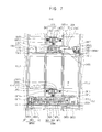
- FIG. 7 is a top plan view of an alternative exemplary embodiment of the touch substrate according to the present invention.
- FIG. 8 is an equivalent circuit diagram illustrating the touch substrate of FIG. 7 .
- FIG. 9 is a cross-sectional view taken along line III-III′ of FIG. 7 .
- FIG. 10 is a cross-sectional view taken along line IV-IV′ of FIG. 7 .
- FIG. 7 An alternative exemplary embodiment of the display apparatus including the touch substrate in FIG. 7 is substantially the same as the display apparatus 1000 shown in FIG. 1 except for the touch substrate 600 .
- the touch substrate 600 in FIG. 7 is substantially the same as the touch substrate 200 shown in FIG. 2 except for a first variable voltage part 610 and a second variable touch substrate 620 .
- the same or like elements shown in FIG. 7 have been labeled with the same reference characters as used above to describe the exemplary embodiment of the touch substrate 200 in FIG. 2 , and any repetitive detailed description thereof will hereinafter be omitted or simplified.
- an exemplary embodiment of the touch substrate 600 includes a first switching element SWTR 1 , a first sensing element STR 1 , the first variable voltage part 610 , a second switching element SWTR 2 , a second sensing element STR 2 and the second variable voltage part 620 .
- the first variable voltage part 610 is electrically connected to a first sensing gate electrode SG 1 of the first sensing element STR 1 to provide a variable gate voltage.
- the first variable voltage part 610 may include a first common active pattern CAP 1 , a first input electrode 612 , a first common output electrode 614 , a second input electrode 616 and a second light blocking pattern BP 2 .
- the first common active pattern CAP 1 may be disposed under the first input electrode 612 , the first common output electrode 614 and the second input electrode 616 .
- the first common active pattern CAP 1 includes a second semiconductor layer 232 and a second ohmic contact layer 234 .
- the second semiconductor layer 232 may include the a-SiGe, and the second ohmic contact layer 234 may include the n+ a-Si.
- the first input electrode 612 is electrically connected to a first bias voltage line BVL 1 through a fourth contact hole CNT 4 to receive a first bias voltage.
- the first common output electrode 614 is disposed apart from the first and second input electrodes 612 and 616 between the first and second input electrodes 612 and 616 .
- the first common output electrode is electrically connected to the first sensing gate electrode SG 1 through a fifth contact hole CNT 5 .
- the second input electrode 616 is electrically connected to the second bias voltage line BVL 2 through a sixth contact hole CNT 6 to receive a second bias voltage.
- a first photo conductor PC 1 (in FIG. 8 ) is collectively defined by the first common active pattern CAP 1 , the first input electrode 612 , and the first common output electrode 614 .
- a second photo conductor PC 2 (in FIG. 8 ) is collectively defined by the first common active pattern CAP 1 , the second input electrode 616 and the first common output electrode 614 .
- the first variable voltage part 610 may have a structure including the first and second photo conductors PC 1 and PC 2 connected to the first sensing gate electrode SG 1 in parallel.
- the second light blocking pattern BP 2 is disposed under the first photo conductor PC 1 .
- the second light blocking pattern BP 2 blocks the infrared light irradiated to the first photo conductor PC 1 .
- a resistance of the first photo conductor PC 1 is substantially uniformly maintained.
- a resistance of the second photo conductor PC 2 is decreased substantially in proportion to an amount of the infrared light irradiated to the second photo conductor PC 2 .
- the second variable voltage part 620 is electrically connected to a second sensing gate electrode SG 2 of the second sensing element STR 2 to provide a variable sensing gate voltage.
- the second variable voltage part 620 may include a second common active pattern CAP 2 , a third input electrode 622 , a second common output electrode 624 , a fourth input electrode 626 and a third light blocking pattern BP 3 .
- the second common active pattern CAP 2 may be disposed under the third input electrode 622 , the second common output electrode 624 and the fourth input electrode 626 .
- the second common active pattern CAP 2 includes a first semiconductor layer 222 and a first ohmic contact layer 224 .
- the first semiconductor layer 222 may include the a-Si
- the first ohmic contact layer 224 may include the n+ a-Si.
- the third input electrode 622 is electrically connected to the first bias voltage line BVL 1 through a ninth contact hole CNT 9 to receive the first bias voltage.
- the second common output electrode 624 is disposed apart from the third and fourth input electrodes 622 and 626 between the third and fourth input electrodes 622 and 626 .
- the second common output electrode is electrically connected to the first sensing gate electrode SG 1 through a tenth contact hole CNT 10 .
- the fourth input electrode 616 is electrically connected to the second bias voltage line BVL 2 through an eleventh contact hole CNT 11 to receive the second bias voltage.
- a third photo conductor PC 3 (in FIG. 8 ) is collectively defined by the second common active pattern CAP 2 , the third input electrode 622 , and the second common output electrode 624 .
- a fourth photo conductor PC 2 (in FIG. 8 ) is collectively defined by the second common active pattern CAP 2 , the fourth input electrode 626 and the second common output electrode 624 .
- the second variable voltage part 620 may have a structure including the third and fourth photo conductors PC 3 and PC 4 connected to the second sensing gate electrode SG 2 in parallel.
- the third light blocking pattern BP 3 is disposed under the third photo conductor PC 3 .
- the third light blocking pattern BP 3 blocks the visible light irradiated to the third photo conductor PC 3 .
- a resistance of the third photo conductor PC 3 may be substantially uniformly maintained.
- a resistance of the fourth photo conductor PC 4 is decreased substantially in proportion to an amount of the visible light irradiated to the fourth photo conductor PC 4 .
- An exemplary embodiment of a method of manufacturing the touch substrate 600 in FIG. 7 is substantially the same as the exemplary embodiment of the method of manufacturing the touch substrate 200 shown in FIGS. 6A to 6F except for the first and second variable voltage parts 610 and 620 . Thus, any repetitive explanation thereof will hereinafter be omitted or simplified.
- a second gate metal pattern is provided, e.g., formed, on the second base substrate 201 after forming the first, fourth, fifth and sixth contact holes CNT 1 , CNT 4 , CNT 5 and CNT 6 on the second base substrate 201 .
- a second gate metal layer is provided, e.g., formed, on the second base substrate on which the first, fourth, fifth and sixth contact holes CNT 1 , CNT 4 , CNT 5 and CNT 6 are formed.
- the second gate metal layer may be patterned to form the second gate metal pattern.
- the second gate metal pattern may include the first top gate electrode TG 1 and the first sensing gate electrode SG 1 .
- the black matrix BM, the color filter layer CF, the overcoat layer OC and the common electrode CE are provided on the base substrate 201 on which the second gate metal pattern is disposed. Therefore, the touch substrate 600 in FIG. 7 may be manufactured as described above.
- a structure of the first and second variable voltage parts 610 and 620 of touch substrate in FIG. 7 may be more simplified than a structure of the first and second variable voltage parts 240 and 260 of the touch substrate 200 in FIG. 2 .
- a sample display apparatus including a first variable voltage part of FIG. 2 was prepared.
- a first bias voltage applied to a first variable source electrode of the first variable voltage part was fixed at 5 volt (V) and a second bias voltage applied to a second variable source electrode of the first variable voltage part was varied from ⁇ 20 V to 20 V, a sensing gate voltage applied to a first sensing gate electrode was measured.
- FIG. 11 is a graph illustrating a change of the sensing gate voltage (V) of an exemplary embodiment of the first variable voltage part according to the second bias voltage.
- X axis represents the second bias voltage
- Y axis represents the sensing gate voltage
- the sensing gate voltage was about ⁇ 8.2 V when an infrared light was not received (Hereinafter, it is referred as a “dark status”), and about 3.8 V when the infrared light was received (Hereinafter, it is referred as a “photo status”).
- the sensing gate voltage was about 3.6 V in the dark status, and about 5 V in the photo status. Accordingly, the first variable voltage part may increase when the infrared light is received.
- FIGS. 12A and 12B are graphs illustrating a current-voltage characteristic of an exemplary embodiment of the first sensing element.
- X axis represents the sensing gate voltage
- Y axis represents a drain current of the first sensing element
- the sensing gate voltage of about ⁇ 6 V is applied to the first sensing gate electrode.
- the sensing gate voltage of about 4 V is applied to the first sensing gate electrode.
- a dark current of the first sensing element is about 7.88 ⁇ 10 ⁇ 12 ampere (A) in the dark status.
- the sensing gate voltage of about ⁇ 6 V is applied to the first sensing gate electrode
- a photo current of the first sensing element is about 4.43 ⁇ 10 ⁇ 8 A in the photo status.
- the sensing gate voltage of about 4 V is applied to the first sensing gate electrode
- a photo current of the first sensing element is about 1.24 ⁇ 10 ⁇ 7 A in the photo status.
- a ratio of the photo current to the dark current was about 5,617.
- a ratio of the photo current to the dark current was about 15,706.
- the ratio of the photo current to the dark current of the first sensing element having the voltage-current characteristic of FIG. 12A is increased by about 2.7 times as the sensing gate voltage increases from about ⁇ 6 V to about 4 V.
- a dark current of the first sensing element is about 3.00 ⁇ 10 ⁇ 13 A in the dark status.
- a photo current of the first sensing element is about 3.22 ⁇ 10 ⁇ 10 A in the photo status.
- a photo current of the first sensing element was about 1.82 ⁇ 10 ⁇ 8 A in the photo status.
- a ratio of the photo current to the dark current was about 1,072.
- a ratio of the photo current to the dark current is about 60,830.
- the ratio between the photo current and the dark current of the first sensing element having the voltage-current characteristic of FIG. 12B is increased about 56 times as the sensing gate voltage increase from ⁇ 6 V to 4 V.
- the sensing gate voltage applied to the first and second sensing elements of the illustrated exemplary embodiments may be adjusted to substantially increase a ratio between the dark current in the dark status and the photo current in the photo status.
- the sensitivity of the first and second sensing elements may be substantially improved.
Landscapes
- Engineering & Computer Science (AREA)
- General Engineering & Computer Science (AREA)
- Theoretical Computer Science (AREA)
- Human Computer Interaction (AREA)
- Physics & Mathematics (AREA)
- General Physics & Mathematics (AREA)
- Solid State Image Pick-Up Elements (AREA)
- Position Input By Displaying (AREA)
- Thin Film Transistor (AREA)
- Liquid Crystal (AREA)
Abstract
Description
Claims (19)
Applications Claiming Priority (3)
| Application Number | Priority Date | Filing Date | Title |
|---|---|---|---|
| KR10-2010-0075968 | 2010-08-06 | ||
| KR1020100075968A KR101699470B1 (en) | 2010-08-06 | 2010-08-06 | Touch substrate and method of manufacturing the same |
| KR2010-0075968 | 2010-08-06 |
Publications (2)
| Publication Number | Publication Date |
|---|---|
| US20120032912A1 US20120032912A1 (en) | 2012-02-09 |
| US8760419B2 true US8760419B2 (en) | 2014-06-24 |
Family
ID=45555790
Family Applications (1)
| Application Number | Title | Priority Date | Filing Date |
|---|---|---|---|
| US13/028,283 Active 2033-02-24 US8760419B2 (en) | 2010-08-06 | 2011-02-16 | Touch substrate and method of manufacturing the same |
Country Status (3)
| Country | Link |
|---|---|
| US (1) | US8760419B2 (en) |
| JP (1) | JP5855384B2 (en) |
| KR (1) | KR101699470B1 (en) |
Cited By (1)
| Publication number | Priority date | Publication date | Assignee | Title |
|---|---|---|---|---|
| US20230284490A1 (en) * | 2022-03-04 | 2023-09-07 | Samsung Display Co., Ltd. | Display device |
Families Citing this family (2)
| Publication number | Priority date | Publication date | Assignee | Title |
|---|---|---|---|---|
| JP6241537B2 (en) * | 2014-03-14 | 2017-12-06 | 株式会社島津製作所 | Magnetic particle operation method and magnetic particle operation device |
| KR102562896B1 (en) * | 2016-03-18 | 2023-08-04 | 삼성디스플레이 주식회사 | Display apparatus |
Citations (6)
| Publication number | Priority date | Publication date | Assignee | Title |
|---|---|---|---|---|
| JP2002278504A (en) | 2001-03-19 | 2002-09-27 | Mitsubishi Electric Corp | Self-luminous display |
| US20050116937A1 (en) * | 2003-12-01 | 2005-06-02 | Choi Joon-Hoo | Photosensitive display panel |
| JP2006330649A (en) | 2005-05-30 | 2006-12-07 | Nec Lcd Technologies Ltd | Liquid crystal display device with tablet function |
| JP2008191822A (en) | 2007-02-02 | 2008-08-21 | Hannstar Display Corp | Light receiving element and liquid crystal display device |
| US20080246739A1 (en) * | 2007-04-06 | 2008-10-09 | Uk Chul Choi | Touch Sensitive Display Device, Apparatus and Method for Driving the Same |
| US20100225617A1 (en) * | 2009-03-06 | 2010-09-09 | Yoshimoto Yoshiharu | Position detection device |
Family Cites Families (3)
| Publication number | Priority date | Publication date | Assignee | Title |
|---|---|---|---|---|
| JP4613689B2 (en) * | 2005-05-20 | 2011-01-19 | 三菱電機株式会社 | Display device with built-in optical sensor |
| KR101143007B1 (en) * | 2005-10-26 | 2012-05-08 | 삼성전자주식회사 | Display device |
| JP5043204B2 (en) * | 2009-01-20 | 2012-10-10 | シャープ株式会社 | Liquid crystal display with light intensity sensor |
-
2010
- 2010-08-06 KR KR1020100075968A patent/KR101699470B1/en not_active Expired - Fee Related
-
2011
- 2011-02-16 US US13/028,283 patent/US8760419B2/en active Active
- 2011-08-05 JP JP2011171798A patent/JP5855384B2/en not_active Expired - Fee Related
Patent Citations (6)
| Publication number | Priority date | Publication date | Assignee | Title |
|---|---|---|---|---|
| JP2002278504A (en) | 2001-03-19 | 2002-09-27 | Mitsubishi Electric Corp | Self-luminous display |
| US20050116937A1 (en) * | 2003-12-01 | 2005-06-02 | Choi Joon-Hoo | Photosensitive display panel |
| JP2006330649A (en) | 2005-05-30 | 2006-12-07 | Nec Lcd Technologies Ltd | Liquid crystal display device with tablet function |
| JP2008191822A (en) | 2007-02-02 | 2008-08-21 | Hannstar Display Corp | Light receiving element and liquid crystal display device |
| US20080246739A1 (en) * | 2007-04-06 | 2008-10-09 | Uk Chul Choi | Touch Sensitive Display Device, Apparatus and Method for Driving the Same |
| US20100225617A1 (en) * | 2009-03-06 | 2010-09-09 | Yoshimoto Yoshiharu | Position detection device |
Cited By (1)
| Publication number | Priority date | Publication date | Assignee | Title |
|---|---|---|---|---|
| US20230284490A1 (en) * | 2022-03-04 | 2023-09-07 | Samsung Display Co., Ltd. | Display device |
Also Published As
| Publication number | Publication date |
|---|---|
| JP5855384B2 (en) | 2016-02-09 |
| KR20120013761A (en) | 2012-02-15 |
| KR101699470B1 (en) | 2017-01-24 |
| CN102375600A (en) | 2012-03-14 |
| US20120032912A1 (en) | 2012-02-09 |
| JP2012038314A (en) | 2012-02-23 |
Similar Documents
| Publication | Publication Date | Title |
|---|---|---|
| US10718968B2 (en) | Display device and method for manufacturing the same | |
| US8345207B2 (en) | Thin film transistor array substrate and liquid crystal display device | |
| EP2657975B1 (en) | Liquid crystal display device and method for manufacturing the same | |
| US7682883B2 (en) | Manufacturing method of thin film transistor array substrate and liquid crystal display panel | |
| CN108595041B (en) | touch display panel | |
| US8901691B2 (en) | Touch sensing substrate and method of manufacturing the same | |
| US20090134398A1 (en) | Array substrate for liquid crystal display device | |
| KR101790161B1 (en) | Optical sensor, manufacturing method thereof, and liquid crystal display device comprising optical sensor | |
| US20110234536A1 (en) | Touch screen substrate and method of manufacturing the same | |
| US9128563B2 (en) | Display device and manufacturing method thereof | |
| US9389452B2 (en) | Electrostatic member in forming touch display apparatus and method of manufacturing the same | |
| US9087750B2 (en) | Touch screen substrate, method of manufacturing the same, and display panel including the touch screen substrate | |
| US8581253B2 (en) | Display substrate and method of manufacturing the same | |
| US8760419B2 (en) | Touch substrate and method of manufacturing the same | |
| CN106057841A (en) | Optical sensor and method of manufacture | |
| US20160300867A1 (en) | Array substrate and liquid crystal display module including tft having improved mobility and method of fabricating the same | |
| KR20080059022A (en) | Liquid crystal display device provided with optical sensor and manufacturing method thereof | |
| US20240395828A1 (en) | Display device | |
| CN102789099A (en) | Liquid crystal display pixel structure, array substrate and liquid crystal display device | |
| JP2012137753A (en) | Display device | |
| KR101087242B1 (en) | Thin film transistor element for liquid crystal display device and manufacturing method thereof | |
| CN102375600B (en) | Touch substrate and the method manufacturing this touch substrate | |
| US20080106690A1 (en) | Method for manufacturing a liquid crystal display device | |
| KR20120073863A (en) | Optical sensor, display device including the same and manufacturing method thereof | |
| US8928054B2 (en) | Touch substrate and method of manufacturing the same |
Legal Events
| Date | Code | Title | Description |
|---|---|---|---|
| AS | Assignment |
Owner name: SAMSUNG ELECTRONICS CO., LTD., KOREA, REPUBLIC OF Free format text: ASSIGNMENT OF ASSIGNORS INTEREST;ASSIGNOR:KIM, HEE-JOON;REEL/FRAME:025815/0372 Effective date: 20110119 |
|
| AS | Assignment |
Owner name: SAMSUNG DISPLAY CO., LTD., KOREA, REPUBLIC OF Free format text: ASSIGNMENT OF ASSIGNORS INTEREST;ASSIGNOR:SAMSUNG ELECTRONICS CO., LTD.;REEL/FRAME:029151/0055 Effective date: 20120904 |
|
| STCF | Information on status: patent grant |
Free format text: PATENTED CASE |
|
| FEPP | Fee payment procedure |
Free format text: PAYOR NUMBER ASSIGNED (ORIGINAL EVENT CODE: ASPN); ENTITY STATUS OF PATENT OWNER: LARGE ENTITY |
|
| MAFP | Maintenance fee payment |
Free format text: PAYMENT OF MAINTENANCE FEE, 4TH YEAR, LARGE ENTITY (ORIGINAL EVENT CODE: M1551) Year of fee payment: 4 |
|
| FEPP | Fee payment procedure |
Free format text: MAINTENANCE FEE REMINDER MAILED (ORIGINAL EVENT CODE: REM.); ENTITY STATUS OF PATENT OWNER: LARGE ENTITY |
|
| FEPP | Fee payment procedure |
Free format text: 7.5 YR SURCHARGE - LATE PMT W/IN 6 MO, LARGE ENTITY (ORIGINAL EVENT CODE: M1555); ENTITY STATUS OF PATENT OWNER: LARGE ENTITY |
|
| MAFP | Maintenance fee payment |
Free format text: PAYMENT OF MAINTENANCE FEE, 8TH YEAR, LARGE ENTITY (ORIGINAL EVENT CODE: M1552); ENTITY STATUS OF PATENT OWNER: LARGE ENTITY Year of fee payment: 8 |
|
| FEPP | Fee payment procedure |
Free format text: MAINTENANCE FEE REMINDER MAILED (ORIGINAL EVENT CODE: REM.); ENTITY STATUS OF PATENT OWNER: LARGE ENTITY |