US8745547B1 - Method for making photomask layout - Google Patents
Method for making photomask layout Download PDFInfo
- Publication number
- US8745547B1 US8745547B1 US13/940,096 US201313940096A US8745547B1 US 8745547 B1 US8745547 B1 US 8745547B1 US 201313940096 A US201313940096 A US 201313940096A US 8745547 B1 US8745547 B1 US 8745547B1
- Authority
- US
- United States
- Prior art keywords
- verification step
- correction step
- correction
- buffer region
- verification
- Prior art date
- Legal status (The legal status is an assumption and is not a legal conclusion. Google has not performed a legal analysis and makes no representation as to the accuracy of the status listed.)
- Active
Links
Images


Classifications
-
- G—PHYSICS
- G03—PHOTOGRAPHY; CINEMATOGRAPHY; ANALOGOUS TECHNIQUES USING WAVES OTHER THAN OPTICAL WAVES; ELECTROGRAPHY; HOLOGRAPHY
- G03F—PHOTOMECHANICAL PRODUCTION OF TEXTURED OR PATTERNED SURFACES, e.g. FOR PRINTING, FOR PROCESSING OF SEMICONDUCTOR DEVICES; MATERIALS THEREFOR; ORIGINALS THEREFOR; APPARATUS SPECIALLY ADAPTED THEREFOR
- G03F1/00—Originals for photomechanical production of textured or patterned surfaces, e.g., masks, photo-masks, reticles; Mask blanks or pellicles therefor; Containers specially adapted therefor; Preparation thereof
- G03F1/68—Preparation processes not covered by groups G03F1/20 - G03F1/50
- G03F1/70—Adapting basic layout or design of masks to lithographic process requirements, e.g., second iteration correction of mask patterns for imaging
Definitions
- the present invention relates to the design and manufacture of an integrated circuit (IC), and particularly to a method for making a photomask layout.
- the level of integration of integrated circuits is increased, the demand for increasing the feature density or reducing the pitch size becomes the mainstream in the semiconductor industry, and the key technology is in photolithography.
- the accuracy in the pattern transferring process from a photomask to a wafer is quite important.
- the present invention provides a method for making a photomask layout, with which the CPU run time can be greatly reduced.
- the present invention provides a method for making a photomask layout.
- a graphic data of a photomask is provided.
- a first correction step is performed to the graphic data.
- a first verification step is performed to all of the graphic data which has been subjected to the first correction step, wherein at least one failed pattern not passing the first verification step is found.
- a second correction step is performed to the at least one failed pattern, so as to obtain at least one modified pattern.
- a second verification step is performed only to at least one buffer region covering the at least one modified pattern, wherein the buffer region has an area less than a whole area of the photomask.
- each of the first correction step, the first verification step, the second correction step and the second verification step is executed by a computer.
- the buffer region further covers a region optically affected by the at least one modified pattern.
- each of the at least one buffer region is set to have the same shape and size.
- each of the at least one buffer region is set to have a different shape and size.
- the at least one buffer region is set to have an area about 500% larger than an area of the at least one modified pattern.
- the at least one buffer region is determined by an optical model.
- the first verification step includes a design rule check, a lithography rule check or a combination thereof.
- the second verification step includes a design rule check, a lithography rule check or a combination thereof.
- the first verification step and the second verification step include the same type of rule check.
- the first correction step includes an optical proximity correction (OPC).
- OPC optical proximity correction
- the second correction step includes an OPC.
- the first correction step is executed by a first electronic design automation (EDA) tool
- the second correction step is executed by a second EDA tool different from the first EDA tool.
- EDA electronic design automation
- the first correction step, the first verification step, the second correction step and the second verification step form a close loop.
- FIG. 1 illustrates a process flow for making a photomask layout according to an embodiment of the present invention.
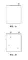
- FIG. 2A to FIG. 2D schematically illustrate a method for making a photomask layout according to an embodiment of the present invention.
- FIG. 1 illustrates a process flow for making a photomask layout according to an embodiment of the present invention.
- FIG. 2A to FIG. 2D schematically illustrate a method for making a photomask layout according to an embodiment of the present invention.
- a graphic data of a photomask is provided in the step S 100 .
- the graphic data is possibly made by an IC designer and stored in a GDS file.
- the photomask is used in an IC process for defining a patterned layer of the IC device.
- the first correction step is performed to the graphic data.
- the graphic data which has been subjected to the first correction step is shown as reference numeral 100 in FIG. 2A .
- the first correction step can be an optical proximity correction (OPC), which may include adding serifs at four corners of a contact hole pattern or adding a hammerhead at an end of a conductive line pattern.
- OPC optical proximity correction
- a first verification step is performed to all of the graphic data 100 which has been subjected to the first correction step, wherein at least one failed pattern 102 not passing the first verification step is found.
- three failed patterns 102 are provided for illustration purposes, but are not construed as limiting the present invention. It is appreciated by people having ordinary skill in the art that only one failed pattern or tens of failed patterns may be possible. Besides, the failed patterns 102 can be the same or different with one another.
- the first verification step may be a process rule check, which includes a lithography rule check (LRC), a design rule check (DRC), or a combination thereof.
- LRC usually includes using numerical integration of a convolution formula to derive the contours of the photomask patterns projected onto the photoresist layer, so as to check if there is any location beyond the lithographic resolution where adjacent patterns are merged in mistake or a single pattern is broken.
- DLC usually includes predicting whether the patterns transferred onto the wafer can meet the requirements of the circuit design or not, according to the above calculated projection contours of the patterns and the variables in etching and alignment.
- the requirements include, for example, sufficient widths for conductive lines, sufficient cross-sectional areas for contact plugs, sufficient overlap areas between conductive lines and contact plugs, prevention of erroneous connection between adjacent patterns due to insufficient etching margin, and so forth.
- the requirements may also include prevention of erroneous connection between the patterns defined by the different photomasks due to insufficient alignment/etching margin.
- a second correction step is performed to the at least one failed pattern 102 , so as to obtain at least one modified pattern 104 .
- the second correction step can be an OPC, which may include adding serifs at four corners of a contact hole pattern or adding a hammerhead at an end of a conductive line pattern.
- the OPC used in the second correction step is different from the OPC used in the first correction step.
- the OPC used in the first correction step can be executed by a first electronic design automation (EDA) tool
- the OPC used in the second correction step can be executed by a second EDA tool
- the first EDA tool is different from the second EDA tool.
- a second verification step is performed only to at least one buffer region 106 covering the at least one modified pattern 104 , wherein the at least one buffer region 106 has an area less than a whole area of the photomask.
- the buffer region 106 can further cover a region optically affected by the at least one modified pattern 104 .
- the buffer region 106 can be determined based on an optical model and marked by an EDA tool the same as or different from the EDA tool of the second verification step.
- each of the at least one buffer region 106 can be set to have the same shape and size, as shown in FIG. 2D .
- each buffer region 106 can be set as a square (1 ⁇ m ⁇ 1 ⁇ m) for ensuring all the patterns adjacent to the corresponding modified pattern 104 are checked and verified.
- each of the at least one buffer region 106 can be set to have a different shape and size as long as the region optically affected by the corresponding modified pattern is covered.
- each of the at one buffer region 106 can be set to have an area about 500% larger than the area of the at least one modified pattern 104 . For example, if the error pattern pitch is 100 nm, the buffer region 106 can be set to be larger than 500 nm at least in one direction, such as having an area of greater than 500 ⁇ 500 nm 2 .
- the second verification step may be a process rule check, which includes a lithography rule check (LRC), a design rule check (DRC), or a combination thereof.
- LRC lithography rule check
- DRC design rule check
- the first verification step and the second verification step include the same type of rule check.
- the first and second verification steps are verified by the LRC.
- the first and second verification steps are verified by the DRC.
- the first and second verification steps are verified by both the LRC and DRC.
- the method of the invention performs the second verification step only to the local buffer regions including and around the modified patterns. Therefore, the CPU run time for performing the second verification step can be improved by about 50% or more.
- each of the first correction step, the first verification step, the second correction step and the second verification step is executed by a computer.
- the first correction step, the first verification step, the second correction step and the second verification step form a close loop, as shown in FIG. 1 .
- the step S 110 to the step S 140 can be performed as many times as needed until the photomask layout meets the customers' requirements.
- a verification step (e.g. the second verification step) is performed only to the patterns which fail to pass the process rule check (e.g. LRC) and are therefore modified, rather than to the whole graphic data including modified and unmodified patterns. Therefore, the CPU run time for the said verification step can be greatly saved and the process cost can be significantly decreased. Accordingly, the design flow of the photomask layout can be simplified to shorten the period needed for manufacturing the photomask.
- the process rule check e.g. LRC
Landscapes
- Physics & Mathematics (AREA)
- General Physics & Mathematics (AREA)
- Preparing Plates And Mask In Photomechanical Process (AREA)
Abstract
Description
Claims (13)
Priority Applications (1)
| Application Number | Priority Date | Filing Date | Title |
|---|---|---|---|
| US13/940,096 US8745547B1 (en) | 2013-07-11 | 2013-07-11 | Method for making photomask layout |
Applications Claiming Priority (1)
| Application Number | Priority Date | Filing Date | Title |
|---|---|---|---|
| US13/940,096 US8745547B1 (en) | 2013-07-11 | 2013-07-11 | Method for making photomask layout |
Publications (1)
| Publication Number | Publication Date |
|---|---|
| US8745547B1 true US8745547B1 (en) | 2014-06-03 |
Family
ID=50781428
Family Applications (1)
| Application Number | Title | Priority Date | Filing Date |
|---|---|---|---|
| US13/940,096 Active US8745547B1 (en) | 2013-07-11 | 2013-07-11 | Method for making photomask layout |
Country Status (1)
| Country | Link |
|---|---|
| US (1) | US8745547B1 (en) |
Citations (25)
| Publication number | Priority date | Publication date | Assignee | Title |
|---|---|---|---|---|
| US6033811A (en) | 1998-01-21 | 2000-03-07 | Lg Semicon Co., Ltd. | Optical proximity correction mask for semiconductor device fabrication |
| US6395438B1 (en) | 2001-01-08 | 2002-05-28 | International Business Machines Corporation | Method of etch bias proximity correction |
| US6470489B1 (en) | 1997-09-17 | 2002-10-22 | Numerical Technologies, Inc. | Design rule checking system and method |
| US6684382B2 (en) | 2001-08-31 | 2004-01-27 | Numerical Technologies, Inc. | Microloading effect correction |
| US6753115B2 (en) | 2001-12-20 | 2004-06-22 | Numerical Technologies, Inc. | Facilitating minimum spacing and/or width control optical proximity correction |
| US6763514B2 (en) | 2001-12-12 | 2004-07-13 | Numerical Technologies, Inc. | Method and apparatus for controlling rippling during optical proximity correction |
| US6852453B2 (en) | 2002-06-06 | 2005-02-08 | Macronix International Co., Ltd. | Fabrication method for semiconductor hole |
| US6961920B2 (en) | 2003-09-18 | 2005-11-01 | International Business Machines Corporation | Method for interlayer and yield based optical proximity correction |
| US20060066339A1 (en) * | 2004-09-06 | 2006-03-30 | Janusz Rajski | Determining and analyzing integrated circuit yield and quality |
| US20060085772A1 (en) * | 2004-10-15 | 2006-04-20 | Youping Zhang | Model-based pattern characterization to generate rules for rule-model-based hybrid optical proximity correction |
| US20060161452A1 (en) | 2004-01-29 | 2006-07-20 | Kla-Tencor Technologies Corp. | Computer-implemented methods, processors, and systems for creating a wafer fabrication process |
| US7213226B2 (en) | 2003-08-20 | 2007-05-01 | Kabushiki Kaisha Toshiba | Pattern dimension correction method and verification method using OPC, mask and semiconductor device fabricated by using the correction method, and system and software product for executing the correction method |
| US7386829B2 (en) | 2003-12-31 | 2008-06-10 | Dongbu Electronics Co., Ltd. | Method of fabricating a photomask |
| US7412676B2 (en) | 2000-06-13 | 2008-08-12 | Nicolas B Cobb | Integrated OPC verification tool |
| US20090193385A1 (en) | 2008-01-25 | 2009-07-30 | Yu-Shiang Yang | Method of checking and correcting mask pattern |
| US20090278569A1 (en) | 2005-04-26 | 2009-11-12 | Hironobu Taoka | Semiconductor Device and its Manufacturing Method, Semiconductor Manufacturing Mask, and Optical Proximity Processing Method |
| US7624369B2 (en) | 2006-10-31 | 2009-11-24 | International Business Machines Corporation | Closed-loop design for manufacturability process |
| US20090300576A1 (en) | 2008-05-27 | 2009-12-03 | Chia-Wei Huang | Method for amending layout patterns |
| US20100036644A1 (en) | 2008-08-07 | 2010-02-11 | Yu-Shiang Yang | Method for selectively amending layout patterns |
| US20100070944A1 (en) | 2008-09-16 | 2010-03-18 | United Microelectronics Corp. | Method for constructing opc model |
| US20100086862A1 (en) | 2008-10-07 | 2010-04-08 | United Microelectronics Corp. | Mask pattern correction and layout method |
| US20100131914A1 (en) * | 2008-11-27 | 2010-05-27 | Te-Hung Wu | Method to determine process window |
| US20100175041A1 (en) | 2009-01-05 | 2010-07-08 | International Business Machines Corporation | Adjustment of mask shapes for improving printability of dense integrated circuit layout |
| US20110029939A1 (en) * | 2009-07-30 | 2011-02-03 | Yu-Shiang Yang | Method for correcting layout pattern |
| US7945871B2 (en) | 2000-06-13 | 2011-05-17 | Cobb Nicolas B | Integrated OPC verification tool |
-
2013
- 2013-07-11 US US13/940,096 patent/US8745547B1/en active Active
Patent Citations (25)
| Publication number | Priority date | Publication date | Assignee | Title |
|---|---|---|---|---|
| US6470489B1 (en) | 1997-09-17 | 2002-10-22 | Numerical Technologies, Inc. | Design rule checking system and method |
| US6033811A (en) | 1998-01-21 | 2000-03-07 | Lg Semicon Co., Ltd. | Optical proximity correction mask for semiconductor device fabrication |
| US7945871B2 (en) | 2000-06-13 | 2011-05-17 | Cobb Nicolas B | Integrated OPC verification tool |
| US7412676B2 (en) | 2000-06-13 | 2008-08-12 | Nicolas B Cobb | Integrated OPC verification tool |
| US6395438B1 (en) | 2001-01-08 | 2002-05-28 | International Business Machines Corporation | Method of etch bias proximity correction |
| US6684382B2 (en) | 2001-08-31 | 2004-01-27 | Numerical Technologies, Inc. | Microloading effect correction |
| US6763514B2 (en) | 2001-12-12 | 2004-07-13 | Numerical Technologies, Inc. | Method and apparatus for controlling rippling during optical proximity correction |
| US6753115B2 (en) | 2001-12-20 | 2004-06-22 | Numerical Technologies, Inc. | Facilitating minimum spacing and/or width control optical proximity correction |
| US6852453B2 (en) | 2002-06-06 | 2005-02-08 | Macronix International Co., Ltd. | Fabrication method for semiconductor hole |
| US7213226B2 (en) | 2003-08-20 | 2007-05-01 | Kabushiki Kaisha Toshiba | Pattern dimension correction method and verification method using OPC, mask and semiconductor device fabricated by using the correction method, and system and software product for executing the correction method |
| US6961920B2 (en) | 2003-09-18 | 2005-11-01 | International Business Machines Corporation | Method for interlayer and yield based optical proximity correction |
| US7386829B2 (en) | 2003-12-31 | 2008-06-10 | Dongbu Electronics Co., Ltd. | Method of fabricating a photomask |
| US20060161452A1 (en) | 2004-01-29 | 2006-07-20 | Kla-Tencor Technologies Corp. | Computer-implemented methods, processors, and systems for creating a wafer fabrication process |
| US20060066339A1 (en) * | 2004-09-06 | 2006-03-30 | Janusz Rajski | Determining and analyzing integrated circuit yield and quality |
| US20060085772A1 (en) * | 2004-10-15 | 2006-04-20 | Youping Zhang | Model-based pattern characterization to generate rules for rule-model-based hybrid optical proximity correction |
| US20090278569A1 (en) | 2005-04-26 | 2009-11-12 | Hironobu Taoka | Semiconductor Device and its Manufacturing Method, Semiconductor Manufacturing Mask, and Optical Proximity Processing Method |
| US7624369B2 (en) | 2006-10-31 | 2009-11-24 | International Business Machines Corporation | Closed-loop design for manufacturability process |
| US20090193385A1 (en) | 2008-01-25 | 2009-07-30 | Yu-Shiang Yang | Method of checking and correcting mask pattern |
| US20090300576A1 (en) | 2008-05-27 | 2009-12-03 | Chia-Wei Huang | Method for amending layout patterns |
| US20100036644A1 (en) | 2008-08-07 | 2010-02-11 | Yu-Shiang Yang | Method for selectively amending layout patterns |
| US20100070944A1 (en) | 2008-09-16 | 2010-03-18 | United Microelectronics Corp. | Method for constructing opc model |
| US20100086862A1 (en) | 2008-10-07 | 2010-04-08 | United Microelectronics Corp. | Mask pattern correction and layout method |
| US20100131914A1 (en) * | 2008-11-27 | 2010-05-27 | Te-Hung Wu | Method to determine process window |
| US20100175041A1 (en) | 2009-01-05 | 2010-07-08 | International Business Machines Corporation | Adjustment of mask shapes for improving printability of dense integrated circuit layout |
| US20110029939A1 (en) * | 2009-07-30 | 2011-02-03 | Yu-Shiang Yang | Method for correcting layout pattern |
Similar Documents
| Publication | Publication Date | Title |
|---|---|---|
| US8278762B2 (en) | Method of manufacturing photomask and method of repairing optical proximity correction | |
| US8788983B2 (en) | Method for correcting layout pattern and mask thereof | |
| US8307310B2 (en) | Pattern generating method, method of manufacturing semiconductor device, computer program product, and pattern-shape-determination-parameter generating method | |
| US20130232456A1 (en) | Optical proximity correction methods for masks to be used in multiple patterning processes | |
| US7730445B2 (en) | Pattern data verification method for semiconductor device, computer-readable recording medium having pattern data verification program for semiconductor device recorded, and semiconductor device manufacturing method | |
| CN106338883B (en) | Optical proximity correction method | |
| US8782572B1 (en) | Method of optical proximity correction | |
| JP2004302263A (en) | Mask pattern correction method and photomask | |
| US8443309B2 (en) | Multifeature test pattern for optical proximity correction model verification | |
| US20090119635A1 (en) | Mask pattern correction method for manufacture of semiconductor integrated circuit device | |
| TWI588595B (en) | Method of optical proximity correction | |
| TWI575308B (en) | Method of correcting assist features | |
| US20110179391A1 (en) | Leakage aware design post-processing | |
| CN104166304B (en) | Method for correcting auxiliary pattern | |
| US12510819B2 (en) | Optical proximity correction system and operating method | |
| US7765518B2 (en) | System and method for implementing optical rule checking to identify and quantify corner rounding errors | |
| US8910090B2 (en) | Methods involving pattern matching to identify and resolve potential non-double-patterning-compliant patterns in double patterning applications | |
| US8701052B1 (en) | Method of optical proximity correction in combination with double patterning technique | |
| US9524362B2 (en) | Method of decomposing layout for generating patterns on photomasks | |
| CN101989309A (en) | How to correct the layout pattern | |
| US8745547B1 (en) | Method for making photomask layout | |
| US8627242B1 (en) | Method for making photomask layout | |
| KR100944332B1 (en) | Method of manufacturing mask of semiconductor device and method of manufacturing semiconductor device | |
| CN101241301A (en) | Method for correcting photomask pattern | |
| US9747404B2 (en) | Method for optimizing an integrated circuit layout design |
Legal Events
| Date | Code | Title | Description |
|---|---|---|---|
| AS | Assignment |
Owner name: UNITED MICROELECTRONICS CORP., TAIWAN Free format text: ASSIGNMENT OF ASSIGNORS INTEREST;ASSIGNORS:KUO, SHIH-MING;CHEN, MING-JUI;HSIEH, TE-HSIEN;AND OTHERS;REEL/FRAME:030823/0773 Effective date: 20130708 |
|
| STCF | Information on status: patent grant |
Free format text: PATENTED CASE |
|
| MAFP | Maintenance fee payment |
Free format text: PAYMENT OF MAINTENANCE FEE, 4TH YEAR, LARGE ENTITY (ORIGINAL EVENT CODE: M1551) Year of fee payment: 4 |
|
| MAFP | Maintenance fee payment |
Free format text: PAYMENT OF MAINTENANCE FEE, 8TH YEAR, LARGE ENTITY (ORIGINAL EVENT CODE: M1552); ENTITY STATUS OF PATENT OWNER: LARGE ENTITY Year of fee payment: 8 |
|
| MAFP | Maintenance fee payment |
Free format text: PAYMENT OF MAINTENANCE FEE, 12TH YEAR, LARGE ENTITY (ORIGINAL EVENT CODE: M1553); ENTITY STATUS OF PATENT OWNER: LARGE ENTITY Year of fee payment: 12 |