US8745337B2 - Apparatus and method for controlling memory overrun - Google Patents
Apparatus and method for controlling memory overrun Download PDFInfo
- Publication number
- US8745337B2 US8745337B2 US12/340,198 US34019808A US8745337B2 US 8745337 B2 US8745337 B2 US 8745337B2 US 34019808 A US34019808 A US 34019808A US 8745337 B2 US8745337 B2 US 8745337B2
- Authority
- US
- United States
- Prior art keywords
- memory
- legacy
- address value
- ate
- address
- Prior art date
- Legal status (The legal status is an assumption and is not a legal conclusion. Google has not performed a legal analysis and makes no representation as to the accuracy of the status listed.)
- Active, expires
Links
Images


Classifications
-
- G—PHYSICS
- G06—COMPUTING OR CALCULATING; COUNTING
- G06F—ELECTRIC DIGITAL DATA PROCESSING
- G06F12/00—Accessing, addressing or allocating within memory systems or architectures
- G06F12/02—Addressing or allocation; Relocation
-
- G—PHYSICS
- G06—COMPUTING OR CALCULATING; COUNTING
- G06F—ELECTRIC DIGITAL DATA PROCESSING
- G06F11/00—Error detection; Error correction; Monitoring
- G06F11/22—Detection or location of defective computer hardware by testing during standby operation or during idle time, e.g. start-up testing
- G06F11/26—Functional testing
- G06F11/261—Functional testing by simulating additional hardware, e.g. fault simulation
Definitions
- the present invention relates generally to memory control and more specifically to memory control for emulating overrun behavior of another memory having equal or lesser capacity.
- ATE Automatic test equipment plays a role in the manufacture of semiconductor devices and circuit board assemblies.
- Manufacturers generally use automatic test equipment, or “testers,” to verify the operation of devices during the manufacturing process. Such devices are referred to as a “device under test” (DUT) or a “unit under test” (UUT).
- DUT device under test
- UUT unit under test
- Early detection of faults eliminates costs that would otherwise be incurred by processing defective devices, and thus reduces the overall cost of manufacturing.
- Manufacturers also use ATE to grade various specifications. Devices can be tested and binned according to different levels of performance in areas, such as speed. Devices can be labeled and sold according to their actual levels of performance.
- legacy ATEs have been replaced with newer, higher-performance ATEs.
- newer testers have many new features
- many of the test programs that run on these newer testers have already been written, and depend on the performance characteristics of legacy ATEs.
- a newer ATE may not necessarily have the same performance characteristics as the legacy ATE. This can affect how existing programs are used with newer, or successor, ATE.
- memory was scarce. Older bus standards also made filling and retrieving memory time-consuming. So, while some test engineers would inadvertently overrun available memory, others would intentionally use undocumented features to loop around, overwrite, or otherwise re-use memory locations.
- the present invention includes methods and apparatus for emulating behavior of a legacy test system.
- provisions are disclosed for newer, higher-performance ATEs to allow legacy programs running on the newer ATE to handle memory overrun situations according to a particular legacy system.
- legacy ATE programs can be used to write to electronic memories of newer, or successor, ATE that would tend to be larger than electronic memories of legacy ATE as if the memory were the size of the legacy memory and with a selectable memory overrun feature that mimics the legacy memory.
- the process described herein relates to a process for transacting data with an addressable memory.
- the process includes receiving a target-address of a requested memory transaction. Whether the received target-address value is greater than a maximum legacy-address value is determined.
- a legacy-memory transaction is emulated in response to a determination that the received target-address value is greater than the maximum legacy-address value.
- a standard memory transaction is performed in response to a determination that the target-address value is not greater than the maximum legacy-address value.
- legacy memory emulation is inhibits the requested memory transaction.
- the legacy memory allows the requested memory transaction at the maximum-legacy address value.
- the legacy memory also allows the requested memory transaction at an overrun-adjusted address value determined by a wrapping of the target address with respect to the maximum-legacy address value.
- the legacy memory emulation is selectable from one or more of the above.
- the device described herein relates to a memory-address filter including an input adapted to receive a target-address of a requested memory transaction and an output in communication with an addressable memory.
- the memory-address filter also includes a legacy-memory emulator in communication with the input and the output.
- the legacy-memory emulator emulates a legacy memory transaction in response to the received target-address value being greater than a maximum legacy-address value. Otherwise, the legacy-memory emulator performs a standard memory transaction.
- the legacy-memory emulator comprises an inhibitor, inhibiting the requested memory transaction.
- the legacy-memory emulator comprises circuitry allowing the requested memory transaction at the maximum-legacy address value.
- the legacy-memory emulator comprises circuitry determining an overrun-adjusted address value according to a wrapping of the target address with respect to the maximum-legacy address value.
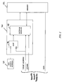
- FIG. 1 is a block diagram of ATE components that may be used to produce a memory overrun handler that emulates memory overrun handling of a desired legacy memory.
- FIG. 2 is a functional block diagram of exemplary memory overrun device according to the present invention.
- FIG. 3 is a flow diagram of an exemplary process for emulating a legacy overrun response according to the present invention.
- FIG. 4 is a schematic diagram of one embodiment of memory overrun circuitry according to the present invention.
- FIG. 5 is a flow diagram of an exemplary process for selectively controlling memory overrun according to the present invention.
- FIG. 6 is a schematic diagram of an alternative embodiment of memory overrun circuitry according to the present invention.
- the tester 10 may be a successor to legacy ATE, such as a newer model of existing ATE, or a completely new model of ATE. These components may be used in the tester 10 to emulate the memory access conditions of legacy ATE. These memory access conditions may include an assignable maximum legacy-address value, or memory depth, that can be equal to or lesser than the available memory capacity.
- the tester 10 may include a test program 12 that may, in turn, be designed for use with the legacy ATE (not shown). In the tester 10 , the test program 12 is used to perform tests on signals received from a DUT 14 over a communication channel 16 .
- a test instrument, such as the stored pattern test instrument 18 shown may be executed through a combination of software, firmware, and or hardware. Alternatively or in addition, the test instrument 18 may be used for controlling the programming of test parameters on the tester 10 .
- test signals may be output from the tester 10 to the DUT 14 over the communications channel 16 .
- the DUT 14 may respond by providing response signals over the communication channel 16 .
- the response signals may be, e.g., produced by the DUT 14 in response to the test signals provided by the tester 10 .
- the signals may be provided from the DUT 14 to the communication channel 16 that are independent of the test signals.
- Such activity over the communication channel 16 can be accomplished by one or more channel cards 20 .
- Each channel card 20 may include one or more of a driver 22 A with associated drive control logic 24 A and receiver, or detector 22 B associated with detector control logic 24 B. There may be one or more detectors 22 B per channel 16 (only one channel 16 is shown in FIG. 1 ).
- the detector 22 B may include one or more comparators and/or other types of hardware to implement a measurement function. At least part of the detector control logic 24 B may also be implemented in software.
- the detector 22 B is in electrical communication with the communications channel 16 , and is configured to receive signals from the communication channel 16 , to compare those signals to one or more thresholds, and to provide comparison results to the test program 12 . There, the comparison results are evaluated in order to determine, e.g., if the DUT 14 has passed or failed a particular test.
- One or more of the channel cards 20 are in communication with a memory 26 .
- the memory 26 includes one or more of a test instruction memory 28 A and a test result memory 28 B.
- One or more of the memories 28 A, 28 B may be a random access memory (RAM).
- the address filter 30 receives a maximum legacy-address value 32 , a target address value associated with a requested memory transaction.
- the transaction may include a write operation in which DATA is written into the addressable memory 34 at a respective address. The writing may be controlled by the STROBE.
- the transaction may include a read operation in which DATA is readable from the addressable memory 34 , from a respective ADDRESS.
- the address filter 30 also receives a strobe.
- the address filter 30 is in further communication with an addressable memory 34 . Transactions with the memory 34 are accomplished according to a filtered address provided by the address filter 30 .
- the address filter 30 includes a comparison element 36 configured to determine whether the target address value is greater than the maximum legacy-address value 32 .
- the comparison element 36 provides an output indicative of the comparison. For example, the comparison element 36 may provide a logical true or false value (e.g., a ‘1’ or a ‘0’) according to the comparison test.
- the address filter 30 further includes a memory overrun handler 38 .
- the overrun handler 38 receives the output of the comparison element 36 .
- the overrun handler 38 emulates a response of a legacy memory.
- the capacity of the addressable memory 34 is greater than or equal to the capacity of the legacy memory.
- such emulation includes inhibiting the requested memory transaction. Such inhibition can be accomplished by inhibiting the strobe signal. Alternatively or in addition, such emulation includes transacting with a memory address equivalent to the maximum legacy-address value.
- the overrun handler 38 filters or otherwise alters the memory address to a value equivalent to a memory address determined by wrapping the target address value according to the maximum legacy-address value. For example, a transaction with the next address after the maximum legacy-address value would be accomplished at a filtered address equivalent to the first memory address.
- the respective address may be subject to alteration by the memory overrun handler 38 .
- the STROBE may also be subject to alteration by the memory overrun handler 38 .
- FIG. 3 illustrates an exemplary flow diagram of a high level memory emulation process 40 according to the present invention.
- a target address is first received at 42 .
- the target address may be intercepted between circuitry requesting a memory transaction and the addressable memory 34 ( FIG. 2 ).
- a determination is made whether the received target address is greater than the maximum legacy-address value at 44 .
- a comparison can be determined whether the received target address is less than or equal to the maximum legacy-address value.
- a legacy response with respect to the requested memory transaction is accomplished at 46 .
- a standard memory transaction at the requested target address value is accomplished at 48 .
- the memory transaction may include a read operation during which data is read from the addressable memory, a write operation during which date is written into the addressable memory, and a combination or read and write operations.
- FIG. 4 An example of a circuit that may be used to emulate memory overrun of legacy ATE, which may be incorporated into the ATE, is shown in the schematic of FIG. 4 .
- the circuit may be part of the ATE 10 ( FIG. 1 ) described above.
- an exemplary memory overrun control circuit 50 is illustrated.
- the memory overrun control circuit 50 is configurable, allowing an addressable electronic memory 52 having storage capacity not less than a legacy electronic memory to emulate the legacy memory in its capacity and its handling of overrun scenarios in which data is written into the memory 52 after the last valid address has been written to.
- the particular example related to an application in which data is written to memory in a sequential manner, as may be the case in a data logger.
- the memory 52 includes a data port 54 .
- the data port 54 may receive data to be written into the memory during a write transaction, or provide data to be read from the memory during a read transaction.
- the memory 52 also receives a data strobe and an address value indicative of a memory address into which the received data should be written upon receipt of the data strobe.
- a resettable address counter 56 is configured to maintain a count value indicative of sequential memory addresses when incremented.
- the address counter 56 can be reset to an initial value indicative of a first memory location (e.g., 0000 0000).
- the address of the first memory location in this example corresponds to zero, the sequential memory addresses need not start or otherwise include zero.
- the sequential memory addresses may start at a non-zero, minimum address and extend to a maximum address, without any restriction as to where in physical memory the span of sequential memory addresses actually resides.
- the circuit 50 includes a first register 58 storing a maximum writable address (DEPTH) of the memory.
- the DEPTH register 58 is configured to store an n-bit memory address word value.
- the circuit includes a second register 60 storing a value (OVEN) indicative of whether a value written to the maximum writable address is overwritten upon subsequent data strobes.
- the circuit 50 also includes a third register 62 storing a value (STOP) indicative of whether further memory writes are disabled after the maximum writable address has been written to.
- values stored in these three registers: DEPTH 58 , OVEN 60 , and STOP 62 determine memory overrun performance of the electronic memory 52 , the performance being configurable by the particular values chosen to emulate a particular legacy memory device.
- the circuit 50 includes a coincidence detector 64 receiving at its inputs output from the address counter 56 and the value stored in the DEPTH register 58 .
- the coincidence detector 64 provides a TRUE value upon the two input values being equal, indicating that the addressed memory location is the last available memory location, as would be the case for an actual legacy memory.
- the coincidence detector 64 can be provided using multiple exclusive OR (XOR) gates, one for each address line, combined through additional gates to provide a single output value according to the logic just described.
- An output of the coincidence detector 64 is fed into a reset terminal 66 of the address counter 56 , causing the counter 56 to be reset to the initial value (e.g., 0000 0000).
- the output of the coincidence detector 64 is also input to one input of a first AND gate 68 .
- the other input of the first AND gate 68 is driven by the value stored in the STOP register 62 .
- An output of the first AND gate 68 drives a D input of a D-type flip-flop 70 .
- a second AND gate 72 is driven by an inverted output of the D-type flip-flop 70 and the data strobe.
- An output of the second AND gate 72 is coupled to a clock input of the address counter 56 .
- the data strobe input drives one input of each of third and fourth AND gates 74 , 76 , the outputs of which are combined in an OR gate 78 .
- the output of the OR gate 78 is coupled to a data strobe input of the electronic memory 52 .
- a second input of the third AND gate 74 is driven by the inverted output of the D-type flip-flop 70 .
- a second input of the fourth AND gate 76 is driven by a value stored in the OVEN register 60 .
- the input to the D-type flip-flop 70 is FALSE, regardless of the value stored in the STOP register 62 .
- the inverted output of the D-type flip-flop 70 is TRUE.
- the output of the second AND gate 72 is thus controlled by the data strobe, allowing the data strobe to clock the address counter 56 , incrementing the address value upon each data strobe.
- the current address value output of the address counter 56 is coupled to the address input of the electronic memory 52 .
- the TRUE output of the D-type flip-flop 70 is also provided to the third AND gate 74 , such that the output of the third AND gate 74 is also controlled by the data strobe.
- the data strobe is applied to the data strobe input of the electronic memory 52 , writing data provided at the data port 54 into the specified addressed location of the electronic memory 52 .
- the address is incremented, and data written into the next memory location, until the memory address coincides with the maximum address value stored in the DEPTH register 58 .
- the coincidence detector 64 provides a TRUE output that resets the address counter 56 and applies the value stored in the STOP register 62 to the input of the D-type flip-flop 70 .
- the STOP value is clocked to the inverted output of the D-type flip-flop 70 , which controls application of the data strobe to the clock input of the address counter 56 and to the data strobe input of the electronic memory 52 .
- the inverted output will be FALSE.
- a STOP value of TRUE disables the clock input to the address counter 56 , and the data strobe input to the electronic memory 52 , unless the overwrite control value stored in the OVEN register 60 is TRUE. If the overwrite control value (OVEN) is TRUE, the data strobe will be applied to the data strobe input of the electronic memory 52 causing data at the data port to be overwritten into the last memory location (i.e., memory location stored in the DEPTH register indicative of a maximum storage location of the legacy memory).
- the data strobe will not be applied to the data strobe input of the electronic memory 52 prohibiting data at the data port from being written into the electronic memory 52 .
- data is read from the same last address for all read addresses above the last address.
- an attempted read from a memory address above the last address is prohibited (e.g., resulting in an error message), the particular performance selected dependent upon the particular legacy memory being emulated.
- the inverted output of the D-type flip-flop 70 will be TRUE regardless of detection of a coincidence by the coincidence detector 64 .
- a STOP value of FALSE enables the clock input to the address counter 56 , and the data strobe into the electronic memory 52 , regardless of any overwrite control value stored in the OVEN register.
- a STOP value of FALSE emulates legacy overrun control referred to as “wrap around.”
- the address counter is reset to the beginning and the data strobe controls the writing of data into the addressed memory location by the electronic memory, incrementing again and overwriting previously written memory values in an incremental fashion.
- the table below summarizes the different emulations of memory overrun control possible with the exemplary circuit providing DEPTH, STOP, and OVEN.
- the tabulated results apply after the address counter output exceeds DEPTH value. While the address is less than DEPTH, data is simply written to the address location upon the next data strobe.
- the memory write control circuitry may be implemented using one or more processing devices.
- processing devices include, but are not limited to, a microprocessor, a microcontroller, programmable logic (e.g., a field-programmable gate array), actual gates, and/or combination(s) thereof.
- programmable logic e.g., a field-programmable gate array
- actual gates e.g., a field-programmable gate array
- combination(s) thereof e.g., a field-programmable gate array
- one or more features of the memory write control functionality of the exemplary memory write control circuitry can be accomplished using instructions executed in a computer program.
- an address is received at step 82 and a data word is received at step 84 .
- the address is compared to a depth value at step 86 , indicative of a maximum legacy memory storage location. If the address is less than the depth value, the data word is written into electronic memory at step 88 and the address counter incremented at step 90 .
- the process flow returns to step 84 for a subsequently received data word.
- a logical value of a STOP value is determined at step 92 . If the logical STOP value is false, indicating wrap-around emulation, the address counter is reset at step 94 , data is written to the reset address value at step 88 , the address counter is incremented at step 90 , and process flow returns to step 84 for another subsequently received data word. If, however, the logical STOP value is true, a logical overwrite enable value (OVEN) is determined at step 96 .
- USN logical overwrite enable value
- step 98 This emulates performance of a legacy memory that terminates further writes upon reaching a maximum storage location. If, however, the logical OVEN value is true, the data is written to the memory address indicative of the maximum storage location at step 100 . Process flow returns to step 84 , with the maximum storage location being overwritten with each received data word. The address depth remains greater than the maximum storage location, and the logical STOP and OVEN values have not changed. This emulates performance of a legacy memory that overwrites the maximum storage location for all data writes addressed to memory address values above the maximum address.
- a memory controller storing such configuration parameters is able to emulate a preferred legacy memory overrun performance.
- Such legacy performance includes wraparound, in which memory addresses above the maximum legacy address are sequentially overwritten into the same memory space, beginning with a first memory location.
- the memory controller is also able to emulate a legacy memory controller that overwrites a maximum memory address for addresses greater than the maximum address, and a legacy memory controller that simply inhibits further memory writes for addresses greater than the maximum address.
- an exemplary address filter circuit 101 is provided to emulate at least three different behaviors.
- the circuit includes an addressable electronic memory 104 , receiving data at a data input 106 .
- the circuit 101 also includes a comparator 108 receiving a target address value of a requested memory transaction.
- the comparator 108 also receives a “last address” value from a last address storage register 109 .
- the last value is indicative of a maximum last address value.
- the comparator 108 compares the two input values, providing an output indicative of the target address being greater than the last address value.
- the output value is input at one leg of each of a first and second AND gates 110 , 112 .
- a first mode control input value (i.e., STOP) can be stored in a STOP value register 111 .
- the STOP value can be applied to a second input of the first AND gate 110 , such that when the stop value is enabled (e.g., a logical 1), and the output of the comparator is also a true value (e.g., a logical 1), the output of the first AND gate 110 is also a true value (e.g., a logical 1).
- the output of the first AND gate 110 is input to a D-type latch 114 .
- An inverted “Q” latch output is false (e.g., a logical 0) for a true input value.
- a memory access strobe associated with data write request is provided together with the inverted Q output at respective inputs to a third AND gate 116 .
- the strobe is active, as usual, unless the STOP value is enabled and the target address is greater than the last address value. In that instance, the STROBE input is essentially blocked, emulating a legacy memory that blocks memory writes in an overrun situation.
- a second mode control input value (i.e., OVEN) is stored in an overwrite-enabled register 118 .
- the OVEN value is provided at a second input of the second AND gate 112 .
- the output of the second AND gate 112 is a true value (e.g., a logical 1).
- the second AND gate 112 output is input to a selection input of a two-channel multiplexer 120 .
- a true value input selects a second channel of the two-channel multiplexer 120 , coupling the memory address input 121 to the second channel, providing the last address value obtained from the last address value register 109 .
- the first multiplexer channel will be selected, regardless as to whether the target address value is greater than the last address value or not.
- the address value provided at the first multiplexer input is obtained from a modulo-combiner 122 , forming a modulo operation of the target address and the last address value. The effect will be to effectively wrap the target address value about the last address.
- the next highest address after the last address value is the first address—wrapped.
- test program designed for legacy ATE may expect a certain memory capacity, with special provisions for handling memory overrun (i.e., writes to memory beyond the available capacity of a memory.)
- the present invention is by no means limited to legacy memory devices.
- the systems and procedures described herein can be used to emulate any memory, not necessary a so-called legacy memory.
- the system and procedures described herein can be used more generally to control overrun handling of a memory without regard to any other memory device.
Landscapes
- Engineering & Computer Science (AREA)
- Theoretical Computer Science (AREA)
- General Engineering & Computer Science (AREA)
- Physics & Mathematics (AREA)
- General Physics & Mathematics (AREA)
- Computer Hardware Design (AREA)
- Quality & Reliability (AREA)
- Storage Device Security (AREA)
Abstract
Description
| TABLE |
| Memory Overrun Control Configurations. |
| STOP | OVEN | Result | ||
| FALSE | FALSE | Wrap around | ||
| FALSE | TRUE | Wrap around | ||
| TRUE | FALSE | Stop writes at last memory location | ||
| TRUE | TRUE | Last memory location overwritten | ||
Claims (16)
Priority Applications (1)
| Application Number | Priority Date | Filing Date | Title |
|---|---|---|---|
| US12/340,198 US8745337B2 (en) | 2007-12-31 | 2008-12-19 | Apparatus and method for controlling memory overrun |
Applications Claiming Priority (2)
| Application Number | Priority Date | Filing Date | Title |
|---|---|---|---|
| US1840907P | 2007-12-31 | 2007-12-31 | |
| US12/340,198 US8745337B2 (en) | 2007-12-31 | 2008-12-19 | Apparatus and method for controlling memory overrun |
Publications (2)
| Publication Number | Publication Date |
|---|---|
| US20090172310A1 US20090172310A1 (en) | 2009-07-02 |
| US8745337B2 true US8745337B2 (en) | 2014-06-03 |
Family
ID=40800030
Family Applications (1)
| Application Number | Title | Priority Date | Filing Date |
|---|---|---|---|
| US12/340,198 Active 2032-03-05 US8745337B2 (en) | 2007-12-31 | 2008-12-19 | Apparatus and method for controlling memory overrun |
Country Status (1)
| Country | Link |
|---|---|
| US (1) | US8745337B2 (en) |
Cited By (2)
| Publication number | Priority date | Publication date | Assignee | Title |
|---|---|---|---|---|
| US20150070370A1 (en) * | 2011-09-12 | 2015-03-12 | Microsoft Corporation | Memory management techniques |
| US10387356B1 (en) | 2018-10-02 | 2019-08-20 | Teradyne, Inc. | Generating timestamps on a packet-oriented bus |
Families Citing this family (2)
| Publication number | Priority date | Publication date | Assignee | Title |
|---|---|---|---|---|
| JP2014199591A (en) * | 2013-03-29 | 2014-10-23 | 株式会社東芝 | Storage control system, storage control device, and program |
| DE102021203225A1 (en) * | 2021-03-30 | 2022-10-06 | Robert Bosch Gesellschaft mit beschränkter Haftung | Device and method for determining address values |
Citations (22)
| Publication number | Priority date | Publication date | Assignee | Title |
|---|---|---|---|---|
| US4926322A (en) * | 1987-08-03 | 1990-05-15 | Compag Computer Corporation | Software emulation of bank-switched memory using a virtual DOS monitor and paged memory management |
| US5727021A (en) | 1996-04-03 | 1998-03-10 | Teradyne, Inc. | Apparatus and method for providing a programmable delay with low fixed delay |
| US5786825A (en) * | 1995-12-13 | 1998-07-28 | National Semiconductor | Virtual display subsystem in a computer |
| US5887146A (en) | 1995-08-14 | 1999-03-23 | Data General Corporation | Symmetric multiprocessing computer with non-uniform memory access architecture |
| US5946247A (en) * | 1994-05-26 | 1999-08-31 | Mitsubishi Denki Kabushiki Kaisha | Semiconductor memory testing device |
| US6363507B1 (en) | 1998-10-19 | 2002-03-26 | Teradyne, Inc. | Integrated multi-channel analog test instrument architecture providing flexible triggering |
| US20020124039A1 (en) * | 2000-12-29 | 2002-09-05 | Ryo Inoue | Modulo addressing |
| US20020144077A1 (en) * | 2001-03-30 | 2002-10-03 | Andersson Peter Kock | Mechanism to extend computer memory protection schemes |
| US6507920B1 (en) | 1999-07-15 | 2003-01-14 | Teradyne, Inc. | Extending synchronous busses by arbitrary lengths using native bus protocol |
| US6519690B1 (en) * | 1999-08-23 | 2003-02-11 | Advanced Micro Devices, Inc. | Flexible address programming with wrap blocking |
| US20030033499A1 (en) * | 2001-08-10 | 2003-02-13 | Hong-Chi Chou | Method and system for circular addressing with efficient memory usage |
| US20030061497A1 (en) * | 2001-09-27 | 2003-03-27 | Zimmer Vincent J. | Method for providing system integrity and legacy environment emulation |
| US6563352B1 (en) | 2002-03-29 | 2003-05-13 | Teradyne, Inc. | Driver circuit employing high-speed tri-state for automatic test equipment |
| US6807616B1 (en) * | 2001-08-09 | 2004-10-19 | Advanced Micro Devices, Inc. | Memory address checking in a proccesor that support both a segmented and a unsegmented address space |
| US20040268200A1 (en) * | 2003-06-26 | 2004-12-30 | Intel Corporation | Pseudo bus agent to support functional testing |
| US6894505B2 (en) | 2002-08-01 | 2005-05-17 | Teradyne, Inc. | Flexible interface for universal bus test instrument |
| US20060123279A1 (en) * | 2004-11-15 | 2006-06-08 | Cardinell Charles S | Apparatus, system, and method for identifying fixed memory address errors in source code at build time |
| US20070118713A1 (en) * | 2005-11-22 | 2007-05-24 | Guterman Daniel C | Memory system for legacy hosts |
| US20070220241A1 (en) * | 2006-03-20 | 2007-09-20 | Rothman Michael A | Efficient resource mapping beyond installed memory space |
| US7343279B2 (en) | 2002-08-01 | 2008-03-11 | Teradyne, Inc. | Universal approach for simulating, emulating, and testing a variety of serial bus types |
| US20080098272A1 (en) | 2006-09-29 | 2008-04-24 | Teradyne, Inc. | Networked test system |
| US7836219B1 (en) * | 2004-02-10 | 2010-11-16 | Pmc-Sierra Us, Inc. | System and method for authentication of embedded RAID on a host RAID card |
-
2008
- 2008-12-19 US US12/340,198 patent/US8745337B2/en active Active
Patent Citations (24)
| Publication number | Priority date | Publication date | Assignee | Title |
|---|---|---|---|---|
| US4926322A (en) * | 1987-08-03 | 1990-05-15 | Compag Computer Corporation | Software emulation of bank-switched memory using a virtual DOS monitor and paged memory management |
| US5946247A (en) * | 1994-05-26 | 1999-08-31 | Mitsubishi Denki Kabushiki Kaisha | Semiconductor memory testing device |
| US6122756A (en) | 1995-08-14 | 2000-09-19 | Data General Corporation | High availability computer system and methods related thereto |
| US5887146A (en) | 1995-08-14 | 1999-03-23 | Data General Corporation | Symmetric multiprocessing computer with non-uniform memory access architecture |
| US6026461A (en) | 1995-08-14 | 2000-02-15 | Data General Corporation | Bus arbitration system for multiprocessor architecture |
| US5786825A (en) * | 1995-12-13 | 1998-07-28 | National Semiconductor | Virtual display subsystem in a computer |
| US5727021A (en) | 1996-04-03 | 1998-03-10 | Teradyne, Inc. | Apparatus and method for providing a programmable delay with low fixed delay |
| US6363507B1 (en) | 1998-10-19 | 2002-03-26 | Teradyne, Inc. | Integrated multi-channel analog test instrument architecture providing flexible triggering |
| US6507920B1 (en) | 1999-07-15 | 2003-01-14 | Teradyne, Inc. | Extending synchronous busses by arbitrary lengths using native bus protocol |
| US6519690B1 (en) * | 1999-08-23 | 2003-02-11 | Advanced Micro Devices, Inc. | Flexible address programming with wrap blocking |
| US20020124039A1 (en) * | 2000-12-29 | 2002-09-05 | Ryo Inoue | Modulo addressing |
| US20020144077A1 (en) * | 2001-03-30 | 2002-10-03 | Andersson Peter Kock | Mechanism to extend computer memory protection schemes |
| US6807616B1 (en) * | 2001-08-09 | 2004-10-19 | Advanced Micro Devices, Inc. | Memory address checking in a proccesor that support both a segmented and a unsegmented address space |
| US20030033499A1 (en) * | 2001-08-10 | 2003-02-13 | Hong-Chi Chou | Method and system for circular addressing with efficient memory usage |
| US20030061497A1 (en) * | 2001-09-27 | 2003-03-27 | Zimmer Vincent J. | Method for providing system integrity and legacy environment emulation |
| US6563352B1 (en) | 2002-03-29 | 2003-05-13 | Teradyne, Inc. | Driver circuit employing high-speed tri-state for automatic test equipment |
| US6894505B2 (en) | 2002-08-01 | 2005-05-17 | Teradyne, Inc. | Flexible interface for universal bus test instrument |
| US7343279B2 (en) | 2002-08-01 | 2008-03-11 | Teradyne, Inc. | Universal approach for simulating, emulating, and testing a variety of serial bus types |
| US20040268200A1 (en) * | 2003-06-26 | 2004-12-30 | Intel Corporation | Pseudo bus agent to support functional testing |
| US7836219B1 (en) * | 2004-02-10 | 2010-11-16 | Pmc-Sierra Us, Inc. | System and method for authentication of embedded RAID on a host RAID card |
| US20060123279A1 (en) * | 2004-11-15 | 2006-06-08 | Cardinell Charles S | Apparatus, system, and method for identifying fixed memory address errors in source code at build time |
| US20070118713A1 (en) * | 2005-11-22 | 2007-05-24 | Guterman Daniel C | Memory system for legacy hosts |
| US20070220241A1 (en) * | 2006-03-20 | 2007-09-20 | Rothman Michael A | Efficient resource mapping beyond installed memory space |
| US20080098272A1 (en) | 2006-09-29 | 2008-04-24 | Teradyne, Inc. | Networked test system |
Cited By (4)
| Publication number | Priority date | Publication date | Assignee | Title |
|---|---|---|---|---|
| US20150070370A1 (en) * | 2011-09-12 | 2015-03-12 | Microsoft Corporation | Memory management techniques |
| US9158699B2 (en) * | 2011-09-12 | 2015-10-13 | Microsoft Technology Licensing, Llc | Memory management techniques |
| US10114740B2 (en) | 2011-09-12 | 2018-10-30 | Microsoft Technology Licensing, Llc | Memory management techniques |
| US10387356B1 (en) | 2018-10-02 | 2019-08-20 | Teradyne, Inc. | Generating timestamps on a packet-oriented bus |
Also Published As
| Publication number | Publication date |
|---|---|
| US20090172310A1 (en) | 2009-07-02 |
Similar Documents
| Publication | Publication Date | Title |
|---|---|---|
| CN112331253A (en) | Chip testing method, terminal and storage medium | |
| US8170828B2 (en) | Test method using memory programmed with tests and protocol to communicate between device under test and tester | |
| JPH10283274A (en) | Method and device for testing memory | |
| US9711241B2 (en) | Method and apparatus for optimized memory test status detection and debug | |
| US20080016415A1 (en) | Evaluation system and method | |
| US5813043A (en) | Method and system including memory patching utilizing a transmission control signal and circuit | |
| US20080010567A1 (en) | Memory testing | |
| US8745337B2 (en) | Apparatus and method for controlling memory overrun | |
| US8006146B2 (en) | Test apparatus and test method for testing a plurality of devices under test | |
| CN115756984A (en) | Memory test method, device, equipment and storage medium | |
| EP0446534A2 (en) | Method of functionally testing cache tag rams in limited-access processor systems | |
| KR940001146B1 (en) | System for checking comparison check function of information processing device | |
| US4989207A (en) | Automatic verification of kernel circuitry based on analysis of memory accesses | |
| US20030070121A1 (en) | Semiconductor test apparatus and method | |
| US9443615B2 (en) | Methods and apparatuses for memory testing with data compression | |
| CN112506820B (en) | USB port hardware parameter analysis method, device, equipment and storage medium | |
| US7185247B2 (en) | Pseudo bus agent to support functional testing | |
| US7523367B2 (en) | Method and apparatus to verify non-deterministic results in an efficient random manner | |
| CN100446129C (en) | Method and system for memory fault testing | |
| US10916322B2 (en) | Testing memory cells by allocating an access value to a memory access and granting an access credit | |
| CN118016139A (en) | Performance testing method, device, equipment and storage medium | |
| US20030120973A1 (en) | Microprocessor and processing method of microprocessor | |
| US7484147B2 (en) | Semiconductor integrated circuit | |
| US10593419B1 (en) | Failing read count diagnostics for memory built-in self-test | |
| US20090300439A1 (en) | Method and Apparatus for Testing Write-Only Registers |
Legal Events
| Date | Code | Title | Description |
|---|---|---|---|
| AS | Assignment |
Owner name: TERADYNE, INC., MASSACHUSETTS Free format text: ASSIGNMENT OF ASSIGNORS INTEREST;ASSIGNORS:FRICK, LLOYD K.;TRUEBENBACH, ERIC;REEL/FRAME:022304/0686 Effective date: 20090210 |
|
| STCF | Information on status: patent grant |
Free format text: PATENTED CASE |
|
| AS | Assignment |
Owner name: BARCLAYS BANK PLC, NEW YORK Free format text: PATENT SECURITY AGREEMENT;ASSIGNORS:TERADYNE, INC.;LITEPOINT CORPORATION;REEL/FRAME:035507/0116 Effective date: 20150427 |
|
| MAFP | Maintenance fee payment |
Free format text: PAYMENT OF MAINTENANCE FEE, 4TH YEAR, LARGE ENTITY (ORIGINAL EVENT CODE: M1551) Year of fee payment: 4 |
|
| AS | Assignment |
Owner name: EAGLE TEST SYSTEMS, INC., ILLINOIS Free format text: RELEASE OF SECURITY INTEREST IN INTELLECTUAL PROPERTY;ASSIGNOR:BARCLAYS BANK PLC, AS COLLATERAL AGENT;REEL/FRAME:049632/0940 Effective date: 20190627 Owner name: TERADYNE, INC., MASSACHUSETTS Free format text: RELEASE OF SECURITY INTEREST IN INTELLECTUAL PROPERTY;ASSIGNOR:BARCLAYS BANK PLC, AS COLLATERAL AGENT;REEL/FRAME:049632/0940 Effective date: 20190627 Owner name: GENRAD, LLC, MASSACHUSETTS Free format text: RELEASE OF SECURITY INTEREST IN INTELLECTUAL PROPERTY;ASSIGNOR:BARCLAYS BANK PLC, AS COLLATERAL AGENT;REEL/FRAME:049632/0940 Effective date: 20190627 Owner name: NEXTEST SYSTEMS CORPORATION, CALIFORNIA Free format text: RELEASE OF SECURITY INTEREST IN INTELLECTUAL PROPERTY;ASSIGNOR:BARCLAYS BANK PLC, AS COLLATERAL AGENT;REEL/FRAME:049632/0940 Effective date: 20190627 Owner name: ENERGID TECHNOLOGIES CORPORATION, MASSACHUSETTS Free format text: RELEASE OF SECURITY INTEREST IN INTELLECTUAL PROPERTY;ASSIGNOR:BARCLAYS BANK PLC, AS COLLATERAL AGENT;REEL/FRAME:049632/0940 Effective date: 20190627 Owner name: LITEPOINT CORPORATION, CALIFORNIA Free format text: RELEASE OF SECURITY INTEREST IN INTELLECTUAL PROPERTY;ASSIGNOR:BARCLAYS BANK PLC, AS COLLATERAL AGENT;REEL/FRAME:049632/0940 Effective date: 20190627 |
|
| AS | Assignment |
Owner name: TRUIST BANK, GEORGIA Free format text: SECURITY INTEREST;ASSIGNOR:TERADYNE, INC.;REEL/FRAME:052595/0632 Effective date: 20200501 |
|
| MAFP | Maintenance fee payment |
Free format text: PAYMENT OF MAINTENANCE FEE, 8TH YEAR, LARGE ENTITY (ORIGINAL EVENT CODE: M1552); ENTITY STATUS OF PATENT OWNER: LARGE ENTITY Year of fee payment: 8 |
|
| MAFP | Maintenance fee payment |
Free format text: PAYMENT OF MAINTENANCE FEE, 12TH YEAR, LARGE ENTITY (ORIGINAL EVENT CODE: M1553); ENTITY STATUS OF PATENT OWNER: LARGE ENTITY Year of fee payment: 12 |