US8736389B2 - Calibration circuit of a frequency generator, and compensation circuit thereof - Google Patents
Calibration circuit of a frequency generator, and compensation circuit thereof Download PDFInfo
- Publication number
- US8736389B2 US8736389B2 US13/234,108 US201113234108A US8736389B2 US 8736389 B2 US8736389 B2 US 8736389B2 US 201113234108 A US201113234108 A US 201113234108A US 8736389 B2 US8736389 B2 US 8736389B2
- Authority
- US
- United States
- Prior art keywords
- signal
- compensation
- outputting
- coupled
- order
- Prior art date
- Legal status (The legal status is an assumption and is not a legal conclusion. Google has not performed a legal analysis and makes no representation as to the accuracy of the status listed.)
- Active, expires
Links
- 239000013078 crystal Substances 0.000 claims abstract description 30
- 230000010355 oscillation Effects 0.000 claims abstract description 16
- 238000001514 detection method Methods 0.000 claims description 13
- 238000010586 diagram Methods 0.000 description 14
- 239000010453 quartz Substances 0.000 description 8
- VYPSYNLAJGMNEJ-UHFFFAOYSA-N silicon dioxide Inorganic materials O=[Si]=O VYPSYNLAJGMNEJ-UHFFFAOYSA-N 0.000 description 8
- 238000013461 design Methods 0.000 description 2
- 230000004075 alteration Effects 0.000 description 1
- 230000008901 benefit Effects 0.000 description 1
- 230000008859 change Effects 0.000 description 1
- 230000001808 coupling effect Effects 0.000 description 1
- 239000000463 material Substances 0.000 description 1
- 238000005259 measurement Methods 0.000 description 1
- 238000000034 method Methods 0.000 description 1
- 238000012986 modification Methods 0.000 description 1
- 230000004048 modification Effects 0.000 description 1
- 230000000737 periodic effect Effects 0.000 description 1
Images

Classifications
-
- H—ELECTRICITY
- H03—ELECTRONIC CIRCUITRY
- H03L—AUTOMATIC CONTROL, STARTING, SYNCHRONISATION OR STABILISATION OF GENERATORS OF ELECTRONIC OSCILLATIONS OR PULSES
- H03L1/00—Stabilisation of generator output against variations of physical values, e.g. power supply
- H03L1/02—Stabilisation of generator output against variations of physical values, e.g. power supply against variations of temperature only
- H03L1/022—Stabilisation of generator output against variations of physical values, e.g. power supply against variations of temperature only by indirect stabilisation, i.e. by generating an electrical correction signal which is a function of the temperature
- H03L1/023—Stabilisation of generator output against variations of physical values, e.g. power supply against variations of temperature only by indirect stabilisation, i.e. by generating an electrical correction signal which is a function of the temperature by using voltage variable capacitance diodes
-
- H—ELECTRICITY
- H03—ELECTRONIC CIRCUITRY
- H03L—AUTOMATIC CONTROL, STARTING, SYNCHRONISATION OR STABILISATION OF GENERATORS OF ELECTRONIC OSCILLATIONS OR PULSES
- H03L1/00—Stabilisation of generator output against variations of physical values, e.g. power supply
- H03L1/02—Stabilisation of generator output against variations of physical values, e.g. power supply against variations of temperature only
- H03L1/028—Stabilisation of generator output against variations of physical values, e.g. power supply against variations of temperature only of generators comprising piezoelectric resonators
Definitions
- the present invention is related to a calibration circuit and a frequency generator, and particularly to a calibration circuit that can calibrate an oscillation frequency of a crystal oscillator according to a temperature, and a frequency generator that can stably output a frequency not influenced by the temperature.
- Quartz is a naturally piezoelectric material.
- the quartz When an external voltage is applied to upper and lower sides of the quartz, the quartz generates mechanical deformation due to a coupling effect between mechanical and electrical characteristics of the quartz, resulting in a voltage drop being generated across the upper and lower sides of the quartz. If an alternating voltage is applied to the upper and lower sides of the quartz, the quartz can generate periodic oscillations.
- a crystal oscillator composed of quartz has an advantage of high frequency stability, so the crystal oscillator can act as a standard frequency source in various applications, including remote communications, mobile telephone systems, global positioning systems, navigation, remote controls, aerospace industries, high-speed computers, precision measurement instruments, consumer electronics, and other fields for providing accurate frequencies.
- FIG. 1 is a diagram illustrating a frequency f generated by the crystal oscillator varying with a temperature.
- the frequency f generated by the crystal oscillator shifts slightly from a target frequency f 0 with the temperature, where a vertical axis in FIG. 1 is a ratio of a difference ⁇ f between the frequency f and the target frequency f 0 to the target frequency f 0 . Therefore, the crystal oscillator needs a calibration circuit to compensate for a frequency error of the crystal oscillator that varies with the temperature.
- An embodiment provides a calibration circuit of a frequency generator.
- the calibration circuit includes at least two compensation circuits and a comparator.
- the at least two compensation circuits is coupled to an input signal for outputting at least a first compensation signal and a second compensation signal.
- the comparator is coupled to the first compensation signal and the second compensation signal for outputting a calibration signal, where the calibration signal is used for determining an oscillation frequency of a crystal oscillator of the frequency generator.
- the frequency generator includes a crystal oscillator, a temperature detection circuit, and a calibration circuit.
- the crystal oscillator is used for generating an oscillation frequency.
- the temperature detection circuit is used for detecting a temperature to generate an input signal.
- the calibration circuit is coupled to the temperature detection circuit.
- the calibration circuit includes at least two compensation circuits and a comparator.
- the at least two compensation circuits is coupled to the input signal for outputting at least a first compensation signal and a second compensation signal.
- the comparator is coupled to the first compensation signal and the second compensation signal for outputting a calibration signal, where the calibration signal is used for determining the oscillation frequency.
- the multi-order compensation unit includes a first multiplier, a second multiplier, and a first amplifier.
- the first multiplier is coupled to an input signal and an adjustment parameter signal for outputting a first signal.
- the second multiplier is coupled to the input signal, the first signal, and the adjustment parameter signal for outputting a second signal.
- the first amplifier is coupled to the second signal for outputting a compensation signal.
- the multi-order compensation unit includes a first multiplier, a second multiplier, a first amplifier, a third multiplier, and a second amplifier.
- the first multiplier is coupled to an input signal and a adjustment parameter signal for outputting a first signal.
- the second multiplier is coupled to the input signal, the first signal, and the adjustment parameter signal for outputting a second signal.
- the first amplifier is coupled to the second signal for outputting a first compensation signal.
- the third multiplier is coupled to the input signal, the second signal, and the adjustment parameter signal for outputting a third signal.
- the second amplifier is coupled to the third signal for outputting a second compensation signal.
- the multi-order compensation unit includes a first multiplier, a second multiplier, a first amplifier, a third multiplier, a second amplifier, a fourth multiplier, and a third amplifier.
- the first multiplier is coupled to an input signal and a adjustment parameter signal for outputting a first signal.
- the second multiplier is coupled to the input signal, the first signal, and the adjustment parameter signal for outputting a second signal.
- the first amplifier is coupled to the second signal for outputting a first compensation signal.
- the third multiplier is coupled to the input signal, the second signal, and the adjustment parameter signal for outputting a third signal.
- the second amplifier is coupled to the third signal for outputting a second compensation signal.
- the fourth multiplier is coupled to the input signal, the third signal, and the adjustment parameter signal for outputting a fourth signal.
- the third amplifier is coupled to the fourth signal for outputting a third compensation signal.
- the multi-order compensation unit includes a first multiplier, a second multiplier, a first amplifier, a third multiplier, a second amplifier, a fourth multiplier, a third amplifier, a fifth multiplier, and a fourth amplifier.
- the first multiplier is coupled to an input signal and a adjustment parameter signal for outputting a first signal.
- the second multiplier is coupled to the input signal, the first signal, and the adjustment parameter signal for outputting a second signal.
- the first amplifier is coupled to the second signal for outputting a first compensation signal.
- the third multiplier is coupled to the input signal, the second signal, and the adjustment parameter signal for outputting a third signal.
- the second amplifier is coupled to the third signal for outputting a second compensation signal.
- the fourth multiplier is coupled to the input signal, the third signal, and the adjustment parameter signal for outputting a fourth signal.
- the third amplifier is coupled to the fourth signal for outputting a third compensation signal.
- the fifth multiplier is coupled to the input signal, the fourth signal, and the adjustment parameter signal for outputting a fifth signal.
- the fourth amplifier is coupled to the fifth signal for outputting a fourth compensation signal.
- the present invention provides a calibration circuit of a frequency generator and a frequency generator.
- the calibration circuit and the frequency generator utilize at least two compensation circuits to generate at least two compensation signals for compensating a frequency error of a crystal oscillator that varies with a temperature.
- a plurality of compensation units included by each compensation circuit of the at least two compensation circuits can be combinations of compensation units of any order. But, the at least two compensation circuits do not include a second-order compensation unit.
- a third-order compensation unit or a higher than third-order compensation unit of the at least two compensation circuits are realized by a plurality of multipliers and at least one amplifier. Because the plurality of compensation units included by each compensation circuit of the at least two compensation circuits can be combinations of compensation units of any order, the present invention can easily adjust the at least two compensation circuits to reduce design complexity of the at least two compensation circuits and increase compensation accuracy.
- FIG. 1 is a diagram illustrating a frequency generated by the crystal oscillator varying with a temperature.
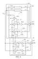
- FIG. 2 is a diagram illustrating a calibration circuit of a frequency generator according to an embodiment.
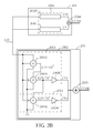
- FIG. 3A , FIG. 3B , and FIG. 3C are diagrams illustrating the first compensation unit group and the second compensation unit group according to different embodiments.
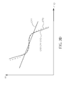
- FIG. 3D is a diagram illustrating the second compensation signal, the third-order compensation signal, and the first-order compensation signal in FIG. 3C versus temperature.
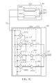
- FIG. 4 is a diagram illustrating a first compensation unit group and a second compensation unit group according to another embodiment.
- FIG. 5 is a diagram illustrating a frequency generator according to another embodiment.
- FIG. 6 is a diagram illustrating a Gilbert-cell type multiplier.
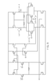
- FIG. 2 is a diagram illustrating a calibration circuit 200 of a frequency generator according to an embodiment.
- the calibration circuit 200 includes two compensation circuits 204 , 206 and a comparator VR.
- the two compensation circuits 204 , 206 are used for describing the present invention, and the present invention is not limited to only the two compensation circuits 204 , 206 .
- a temperature detection circuit 202 is coupled to the two compensation circuits 204 , 206 for detecting a temperature T to generate an input signal LIV, where a linear relationship exists between the input signal LIV and the temperature T.
- the two compensation circuits 204 , 206 are coupled to the input signal LIV, and output a first compensation signal CV 204 and a second compensation signal CV 206 to the comparator VR, respectively, according to the input signal LIV.
- the comparator VR is coupled to the first compensation signal CV 204 and the second compensation signal CV 206 , and outputs a calibration signal CS according to the first compensation signal CV 204 and the second compensation signal CV 206 .
- the calibration signal CS is used for determining an oscillation frequency of a crystal oscillator VCXO, and the crystal oscillator VCXO is a crystal oscillator.
- the comparator VR is a varactor diode, and the comparator VR can change the calibration signal CS according to the first compensation signal CV 204 and the second compensation signal CV 206 . Therefore, the calibration circuit 200 can fine tune a frequency error of the crystal oscillator VCXO that varies with the temperature according to the calibration signal CS that varies with the temperature.
- the calibration circuit 200 can include the temperature detection circuit 202 according to another embodiment.
- the compensation circuit 204 includes a first compensation unit group 2042 and a first adder 2044 .
- the first compensation unit group 2042 includes n compensation units, and the first compensation unit group 2042 is coupled to the input signal LIV for outputting a first compensation unit signal group, where n ⁇ 1.
- the first adder 2044 is coupled to the first compensation unit signal group for generating the first compensation signal CV 204 .
- the compensation circuit 206 includes a second compensation unit group 2062 and a second adder 2070 .
- the second compensation unit group 2062 includes m compensation units for outputting a second compensation unit signal group, where m ⁇ 1.
- the second adder 2070 is coupled to the second compensation unit signal group for generating the second compensation signal CV 206 .
- the n compensation units of the first compensation unit group 2042 and the m compensation units of the second compensation unit group 2062 can be combinations of compensation units of any order. But, the first compensation unit group 2042 and the second compensation unit group 2062 do not include a second-order compensation unit.
- FIG. 3A , FIG. 3B , and FIG. 3C are diagrams illustrating the first compensation unit group 2042 and the second compensation unit group 2062 according to different embodiments.
- the first compensation unit group 2042 includes a zeroth-order compensation unit 20420 , a first-order compensation unit 20421 , and a first adder 2044 , where the zeroth-order compensation unit 20420 is coupled to the input signal LIV for outputting a zeroth-order compensation signal CV 0 according to the input signal LIV.
- the first-order compensation unit 20421 is coupled to the input signal LIV for outputting a first-order compensation signal CV 1 according to the input signal LIV.
- the first adder 2044 is coupled to the zeroth-order compensation signal CV 0 and the first-order compensation signal CV 1 for generating the first compensation signal CV 204 .
- the second compensation unit group 2062 includes a third-order compensation unit 2063 .
- the third-order compensation unit 2063 includes a first multiplier 20632 , a second multiplier 20634 , and a first amplifier 20636 , where the third-order compensation unit 2063 is coupled to the input signal LIV for outputting a third-order compensation signal CV 3 acting as the second compensation signal CV 206 .
- the first multiplier 20632 has a first terminal for receiving the input signal LIV, a second terminal for receiving the input signal LIV, a third terminal for receiving an adjustment parameter signal T 0 , and an output terminal for outputting a first signal (LIV ⁇ T 0 ) 2 .
- the second multiplier 20634 has a first terminal for receiving the input signal LIV, a second terminal for receiving the first signal (LIV ⁇ T 0 ) 2 , a third terminal for receiving the adjustment parameter signal T 0 , and an output terminal for outputting a second signal (LIV ⁇ T 0 ) 3 .
- the first amplifier 20636 has a first terminal coupled to the second multiplier 20634 for receiving the second signal (LIV ⁇ T 0 ) 3 , and an output terminal for outputting a third-order compensation signal CV 3 .
- a (j ⁇ 2)th coefficient COEF (j ⁇ 2) is provided by a (j ⁇ 2)th amplifier, where j ⁇ 3, and j is a positive integer.
- a first coefficient COEF 1 is provided by the first amplifier 20636 , and the first coefficient COEF 1 is a constant value.
- the first multiplier 20632 and the second multiplier 20634 are Gilbert-cell type multipliers (as shown in FIG. 6 ).
- the third-order compensation signal CV 3 is the second compensation signal CV 206 .
- the first compensation unit group 2042 includes the zeroth-order compensation unit 20420 , the first-order compensation unit 20421 , and the first adder 2044 .
- the first compensation unit group 2042 is described in FIG. 3A , so further descriptions thereof are omitted for simplicity.
- the second compensation unit group 2062 includes the third-order compensation unit 2063 and a fourth-order compensation unit 2064 , where the third-order compensation unit 2063 is described in FIG. 3A , so further descriptions thereof are omitted for simplicity.
- the fourth-order compensation unit 2064 includes a third multiplier 20642 and a second amplifier 20644 .
- a second adder 2070 is coupled to the third-order compensation signal CV 3 and a fourth-order compensation signal CV 4 for generating a second compensation signal CV 206 .
- the third multiplier 20642 has a first terminal for receiving the input signal LIV, a second terminal for receiving the second signal (LIV ⁇ T 0 ) 3 , a third terminal for receiving the adjustment parameter signal T 0 , and an output terminal for outputting a third signal (LIV ⁇ T 0 ) 4 .
- the second amplifier 20644 has a first terminal coupled to the third multiplier 20642 for receiving the third signal (LIV ⁇ T 0 ) 4 , and an output terminal for outputting the fourth-order compensation signal CV 4 .
- the fourth-order compensation signal CV 4 is generated according to equation (1), the third signal (LIV ⁇ T 0 ) 4 , and a second coefficient COEF 2 , where the second coefficient COEF 2 is a variable coefficient.
- the third multiplier 20642 is a Gilbert-cell type multiplier (as shown in FIG. 6 ).
- the second compensation signal CV 206 is generated by the second adder 2070 according to equation (3), the third-order compensation signal CV 3 , and the fourth-order compensation signal CV 4 :
- the first compensation unit group 2042 includes the zeroth-order compensation unit 20420 , the first-order compensation unit 20421 , and the first adder 2044 .
- the first compensation unit group 2042 is described in FIG. 3A , so further description thereof is omitted for simplicity.
- the second compensation unit group 2062 includes the third-order compensation unit 2063 , the fourth-order compensation unit 2064 , a fifth-order compensation unit 2065 , and the second adder 2070 , where the second adder 2070 is coupled to the third-order compensation signal CV 3 , the fourth-order compensation signal CV 4 , and a fifth-order compensation signal CV 5 for generating a second compensation signal CV 206 .
- the third-order compensation unit 2063 and the fourth-order compensation unit 2064 are described in FIG. 3B , so further description thereof is omitted for simplicity.
- the fifth-order compensation unit 2065 includes a fourth multiplier 20652 and a third amplifier 20654 .
- the fourth multiplier 20652 has a first terminal for receiving the input signal LIV, a second terminal for receiving the third signal (LIV ⁇ T 0 ) 4 , a third terminal for receiving the adjustment parameter signal T 0 , and an output terminal for outputting a fourth signal (LIV ⁇ T 0 ) 5 .
- the third amplifier 20654 has a first terminal coupled to the fourth multiplier 20652 for receiving the fourth signal (LIV ⁇ T 0 ) 5 , and an output terminal for outputting the fifth-order compensation signal CV 5 .
- the fifth-order compensation signal CV 5 is generated according to equation (1), the fourth signal (LIV ⁇ T 0 ) 5 , and a third coefficient COEF 3 , where the third coefficient COEF 3 is a variable coefficient.
- the fourth multiplier 20652 is a Gilbert-cell type multiplier (as shown in FIG. 6 ).
- the second compensation signal CV 206 is generated by the second adder 2070 according to equation (4), the third-order compensation signal CV 3 , the fourth-order compensation signal CV 4 , and the fifth-order compensation signal CV 5 :
- FIG. 3D is a diagram illustrating the second compensation signal CV 206 (CV 3 +CV 4 +CV 5 ), the third-order compensation signal CV 3 , and the first-order compensation signal CV 1 in FIG. 3C versus the temperature.
- the second compensation signal CV 206 , the third-order compensation signal CV 3 , and the first-order compensation signal CV 1 vary with the temperature. Therefore, a user can flexibly adjust a plurality of compensation units included by the two compensation circuits 204 , 206 to calibrate the frequency error of the crystal oscillator VCXO to vary exactly with the temperature according to the frequency error of the crystal oscillator VCXO that varies with the temperature.
- the first compensation unit group 2042 includes the zeroth-order compensation unit 20420 and the first-order compensation unit 20421 .
- the second compensation unit group 2062 includes the third-order compensation unit 2063 to a kth-order compensation unit 206 k , where k ⁇ 6.
- subsequent operational principles of the kth-order compensation unit 206 k are the same as those of the fourth-order compensation unit 2064 and the fifth-order compensation unit 2065 , so further description thereof is omitted for simplicity.
- FIG. 4 is a diagram illustrating a first compensation unit group 2042 and a second compensation unit group 2062 according to another embodiment.
- the first compensation unit group 2042 includes the zeroth-order compensation unit 20420 , the first-order compensation unit 20421 , the third-order compensation unit 20623 , and the fourth-order compensation unit 20624 .
- the second compensation unit group 2042 includes the fifth-order compensation unit 2065 and a sixth-order compensation unit 2066 , where the sixth-order compensation unit 2066 includes a fifth multiplier 20662 and a fourth amplifier 20664 . Therefore, a first compensation signal CV 204 in FIG.
- CV 204 CV 0 +CV 1+COEF1 ⁇ ( LIV ⁇ T 0) 3 +COEF2 ⁇ ( LIV ⁇ T 0) 4
- CV 206 COEF3 ⁇ ( LIV ⁇ T 0) 5 +COEF4 ⁇ ( LIV ⁇ T 0) 6 (6)
- FIG. 3A , FIG. 3B , FIG. 3C , and FIG. 4 are only used for describing that the first compensation unit group 2042 and the second compensation unit group 2062 can be combinations of compensation units of any order. But, the first compensation unit group 2042 and the second compensation unit group 2062 do not include a second-order compensation unit. Therefore, the present invention is not limited to the embodiments in FIG. 3A , FIG. 3B , FIG. 3C , and FIG. 4 .
- FIG. 5 is a diagram illustrating a frequency generator 500 according to another embodiment.
- the frequency generator 500 includes the temperature detection circuit 202 , the two compensation circuits 204 , 206 , and a crystal oscillator 502 .
- the crystal oscillator 502 is used for outputting an oscillation frequency F not influenced by a temperature. Further, subsequent operational principles of the crystal oscillator 502 of the frequency generator 500 are the same as those of the crystal oscillator VCXO in FIG. 2 , so further descriptions thereof are omitted for simplicity.
- FIG. 6 is a diagram illustrating a Gilbert-cell type multiplier.
- the ith Gilbert-cell type multiplier receives the adjustment parameter signal T 0 , the input signal LIV, and an (i ⁇ 1)th signal (LIV ⁇ T 0 )'
- the ith Gilbert-cell type multiplier outputs an ith signal (LIV ⁇ T 0 ) i ⁇ 1 , where the (i ⁇ 1)th signal (LIV ⁇ T 0 ) i and the ith signal (LIV ⁇ T 0 ) i+1 are determined by equation (7) and equation (8), respectively:
- ( LIV ⁇ T 0) i ( LIV ⁇ T 0) i — P ⁇ ( LIV ⁇ T 0) i — N (7)
- ( LIV ⁇ T 0) i+1 ( LIV ⁇ T 0) i+1 — P ⁇ ( LIV ⁇ T 0) i+1 — N (8)
- (LIV ⁇ T 0 ) i _P and (LIV ⁇ T 0 ) i _N are differential signals of the (i ⁇ 1)th signal (LIV ⁇ T 0 ) i
- (LIV ⁇ T 0 ) i+1 _P and (LIV ⁇ T 0 ) i+1 _N are differential signals of the ith signal (LIV ⁇ T 0 ) i+1 .
- the calibration circuit of the frequency generator and the frequency generator utilize the at least two compensation circuits to generate the at least two compensation signals for compensating the frequency error of the crystal oscillator that varies with the temperature.
- the plurality of compensation units included by each compensation circuit of the at least two compensation circuits can be combinations of compensation units of any order. But, the at least two compensation circuits do not include the second-order compensation unit.
- the third-order compensation unit or the higher than third-order compensation unit of the at least two compensation circuits are realized by a plurality of multipliers and at least one amplifier. Because the plurality of compensation units included by each compensation circuit of the at least two compensation circuits can be combinations of compensation units of any order, the present invention can easily adjust the at least two compensation circuits to reduce design complexity of the at least two compensation circuits and increase compensation accuracy.
Landscapes
- Oscillators With Electromechanical Resonators (AREA)
- Amplifiers (AREA)
- Stabilization Of Oscillater, Synchronisation, Frequency Synthesizers (AREA)
Abstract
Description
CVj=COEF(j−2)×(LIV−T0)j (1)
CV3=COEF1×(LIV−T0)3 (2)
CV206=CV3+CV4=COEF1×(LIV−T0)3+COEF2×(LIV−T0)4 (3)
CV204=CV0+CV1+COEF1×(LIV−T0)3+COEF2×(LIV−T0)4 (5)
CV206=COEF3×(LIV−T0)5+COEF4×(LIV−T0)6 (6)
(LIV−T0)i=(LIV−T0)i — P−(LIV−T0)i — N (7)
(LIV−T0)i+1=(LIV−T0)i+1 — P−(LIV−T0)i+1 — N (8)
Claims (33)
Applications Claiming Priority (3)
| Application Number | Priority Date | Filing Date | Title |
|---|---|---|---|
| TW100110808A | 2011-03-29 | ||
| TW100110808 | 2011-03-29 | ||
| TW100110808A TWI449323B (en) | 2011-03-29 | 2011-03-29 | Calibration circuit of a frequency generator and compensation circuit thereof |
Publications (2)
| Publication Number | Publication Date |
|---|---|
| US20120249256A1 US20120249256A1 (en) | 2012-10-04 |
| US8736389B2 true US8736389B2 (en) | 2014-05-27 |
Family
ID=45655682
Family Applications (1)
| Application Number | Title | Priority Date | Filing Date |
|---|---|---|---|
| US13/234,108 Active 2031-11-03 US8736389B2 (en) | 2011-03-29 | 2011-09-15 | Calibration circuit of a frequency generator, and compensation circuit thereof |
Country Status (4)
| Country | Link |
|---|---|
| US (1) | US8736389B2 (en) |
| EP (1) | EP2506439B1 (en) |
| CN (1) | CN102739155B (en) |
| TW (1) | TWI449323B (en) |
Cited By (2)
| Publication number | Priority date | Publication date | Assignee | Title |
|---|---|---|---|---|
| US20120303307A1 (en) * | 2011-05-25 | 2012-11-29 | Ming-Chung Huang | Circuit and method for detecting oscillating frequency drift |
| US20200059197A1 (en) * | 2016-03-15 | 2020-02-20 | Texas Instruments Incorporated | Temperature compensated oscillator driver |
Families Citing this family (1)
| Publication number | Priority date | Publication date | Assignee | Title |
|---|---|---|---|---|
| CN110212911B (en) * | 2019-06-24 | 2023-04-07 | Oppo广东移动通信有限公司 | Frequency calibration method and device and storage medium |
Citations (7)
| Publication number | Priority date | Publication date | Assignee | Title |
|---|---|---|---|---|
| US4079280A (en) * | 1976-06-02 | 1978-03-14 | Hewlett-Packard Company | Quartz resonator cut to compensate for static and dynamic thermal transients |
| GB2121629A (en) | 1982-05-18 | 1983-12-21 | Standard Telephones Cables Ltd | Temperature controlled crystal oscillator |
| US5481229A (en) | 1994-11-29 | 1996-01-02 | Motorola, Inc. | Low power temperature compensated crystal oscillator |
| JPH08116214A (en) | 1994-10-17 | 1996-05-07 | Fujitsu Ltd | Function generator and oscillation circuit with temperature compensation |
| US6292066B1 (en) | 1997-07-11 | 2001-09-18 | Matsushita Electric Industrial Co., Ltd. | Function generator, crystal oscillation device and method of adjusting crystal oscillation device |
| US7205858B2 (en) * | 2003-08-21 | 2007-04-17 | Murata Manufacturing Co., Ltd. | Temperature compensated piezoelectric oscillator and electronic apparatus comprising it |
| US20080007363A1 (en) | 2006-06-01 | 2008-01-10 | Kei Nagatomo | Function generation circuit |
Family Cites Families (2)
| Publication number | Priority date | Publication date | Assignee | Title |
|---|---|---|---|---|
| US7161340B2 (en) * | 2004-07-12 | 2007-01-09 | Realtek Semiconductor Corp. | Method and apparatus for generating N-order compensated temperature independent reference voltage |
| CN101459428B (en) * | 2007-12-14 | 2011-09-28 | 上海华虹Nec电子有限公司 | Temperature compensation method for D/A converter |
-
2011
- 2011-03-29 TW TW100110808A patent/TWI449323B/en active
- 2011-05-26 CN CN201110140720.4A patent/CN102739155B/en active Active
- 2011-09-15 US US13/234,108 patent/US8736389B2/en active Active
-
2012
- 2012-02-14 EP EP12155265.7A patent/EP2506439B1/en active Active
Patent Citations (7)
| Publication number | Priority date | Publication date | Assignee | Title |
|---|---|---|---|---|
| US4079280A (en) * | 1976-06-02 | 1978-03-14 | Hewlett-Packard Company | Quartz resonator cut to compensate for static and dynamic thermal transients |
| GB2121629A (en) | 1982-05-18 | 1983-12-21 | Standard Telephones Cables Ltd | Temperature controlled crystal oscillator |
| JPH08116214A (en) | 1994-10-17 | 1996-05-07 | Fujitsu Ltd | Function generator and oscillation circuit with temperature compensation |
| US5481229A (en) | 1994-11-29 | 1996-01-02 | Motorola, Inc. | Low power temperature compensated crystal oscillator |
| US6292066B1 (en) | 1997-07-11 | 2001-09-18 | Matsushita Electric Industrial Co., Ltd. | Function generator, crystal oscillation device and method of adjusting crystal oscillation device |
| US7205858B2 (en) * | 2003-08-21 | 2007-04-17 | Murata Manufacturing Co., Ltd. | Temperature compensated piezoelectric oscillator and electronic apparatus comprising it |
| US20080007363A1 (en) | 2006-06-01 | 2008-01-10 | Kei Nagatomo | Function generation circuit |
Cited By (4)
| Publication number | Priority date | Publication date | Assignee | Title |
|---|---|---|---|---|
| US20120303307A1 (en) * | 2011-05-25 | 2012-11-29 | Ming-Chung Huang | Circuit and method for detecting oscillating frequency drift |
| US9000855B2 (en) * | 2011-05-25 | 2015-04-07 | Realtek Semiconductor Corp. | Circuit and method for detecting oscillating frequency drift |
| US20200059197A1 (en) * | 2016-03-15 | 2020-02-20 | Texas Instruments Incorporated | Temperature compensated oscillator driver |
| US11005419B2 (en) * | 2016-03-15 | 2021-05-11 | Texas Instruments Incorporated | Temperature compensated oscillator driver |
Also Published As
| Publication number | Publication date |
|---|---|
| TW201242236A (en) | 2012-10-16 |
| EP2506439B1 (en) | 2021-05-05 |
| CN102739155A (en) | 2012-10-17 |
| TWI449323B (en) | 2014-08-11 |
| CN102739155B (en) | 2016-06-15 |
| EP2506439A1 (en) | 2012-10-03 |
| US20120249256A1 (en) | 2012-10-04 |
Similar Documents
| Publication | Publication Date | Title |
|---|---|---|
| US8536952B2 (en) | Oscillation device | |
| US8686806B2 (en) | Highly accurate temperature stable clock based on differential frequency discrimination of oscillators | |
| US8581671B2 (en) | Oscillation device | |
| US8471619B2 (en) | Circuit and method for generating a clock signal | |
| US7911285B2 (en) | Reference frequency control circuit | |
| JP2017199947A (en) | Circuit device, oscillator, electronic apparatus, and moving body | |
| KR101947611B1 (en) | Electronic oscillation circuit | |
| US8890591B1 (en) | Circuit and method of using time-average-frequency direct period syntheszier for improving crystal-less frequency generator frequency stability | |
| US8736389B2 (en) | Calibration circuit of a frequency generator, and compensation circuit thereof | |
| US11584635B2 (en) | Dual-output microelectromechanical resonator and method of manufacture and operation thereof | |
| US20190035848A1 (en) | Resonator Device, Electronic Apparatus, And Vehicle | |
| CN107733369B (en) | Temperature compensated crystal oscillator | |
| Ahmed et al. | A highly stable CMOS self-compensated oscillator (SCO) based on an LC tank temperature null concept | |
| JP2017212637A (en) | Adjustment device, adjustment method, and oscillation device | |
| US20240171126A1 (en) | Phase locked oscillator and method | |
| Kobayashi et al. | High-performance DSP-TCXO using twin-crystal oscillator | |
| US20190006989A1 (en) | Resonator Device, Electronic Apparatus, And Vehicle | |
| CN115420398A (en) | Temperature sensor and temperature determination method | |
| CN112352143B (en) | Dual output microelectromechanical resonator and methods of manufacturing and operating the same | |
| US9000848B2 (en) | Noise reduction in MEMS oscillators and related apparatus and methods | |
| JP2012216963A (en) | Function generation circuit, control signal generation method, and curve fitting method | |
| US20240223169A1 (en) | Systems and methods for real-time frequency shift detection via a nested-mems architecture | |
| Ishii et al. | A new generation DSP-OCXO using crystal temperature sensor | |
| CN112835285A (en) | Method and device for designing complete passive rubidium atomic clock | |
| JP2011160038A (en) | Method for manufacturing temperature compensation type oscillation circuit, and the temperature compensation type oscillation circuit |
Legal Events
| Date | Code | Title | Description |
|---|---|---|---|
| AS | Assignment |
Owner name: RICHWAVE TECHNOLOGY CORP., TAIWAN Free format text: ASSIGNMENT OF ASSIGNORS INTEREST;ASSIGNORS:WANG, YI-FONG;DENG, WEI-KUNG;REEL/FRAME:026915/0396 Effective date: 20110914 |
|
| STCF | Information on status: patent grant |
Free format text: PATENTED CASE |
|
| MAFP | Maintenance fee payment |
Free format text: PAYMENT OF MAINTENANCE FEE, 4TH YR, SMALL ENTITY (ORIGINAL EVENT CODE: M2551) Year of fee payment: 4 |
|
| MAFP | Maintenance fee payment |
Free format text: PAYMENT OF MAINTENANCE FEE, 8TH YR, SMALL ENTITY (ORIGINAL EVENT CODE: M2552); ENTITY STATUS OF PATENT OWNER: SMALL ENTITY Year of fee payment: 8 |