US8735233B2 - Manufacturing method for thin film semiconductor device, manufacturing method for thin film semiconductor array substrate, method of forming crystalline silicon thin film, and apparatus for forming crystalline silicon thin film - Google Patents
Manufacturing method for thin film semiconductor device, manufacturing method for thin film semiconductor array substrate, method of forming crystalline silicon thin film, and apparatus for forming crystalline silicon thin film Download PDFInfo
- Publication number
- US8735233B2 US8735233B2 US13/451,078 US201213451078A US8735233B2 US 8735233 B2 US8735233 B2 US 8735233B2 US 201213451078 A US201213451078 A US 201213451078A US 8735233 B2 US8735233 B2 US 8735233B2
- Authority
- US
- United States
- Prior art keywords
- thin film
- silicon thin
- laser beam
- intensity distribution
- crystalline silicon
- Prior art date
- Legal status (The legal status is an assumption and is not a legal conclusion. Google has not performed a legal analysis and makes no representation as to the accuracy of the status listed.)
- Expired - Fee Related
Links
Images


Classifications
-
- H—ELECTRICITY
- H10—SEMICONDUCTOR DEVICES; ELECTRIC SOLID-STATE DEVICES NOT OTHERWISE PROVIDED FOR
- H10P—GENERIC PROCESSES OR APPARATUS FOR THE MANUFACTURE OR TREATMENT OF DEVICES COVERED BY CLASS H10
- H10P10/00—Bonding of wafers, substrates or parts of devices
-
- H—ELECTRICITY
- H10—SEMICONDUCTOR DEVICES; ELECTRIC SOLID-STATE DEVICES NOT OTHERWISE PROVIDED FOR
- H10P—GENERIC PROCESSES OR APPARATUS FOR THE MANUFACTURE OR TREATMENT OF DEVICES COVERED BY CLASS H10
- H10P14/00—Formation of materials, e.g. in the shape of layers or pillars
- H10P14/20—Formation of materials, e.g. in the shape of layers or pillars of semiconductor materials
- H10P14/34—Deposited materials, e.g. layers
- H10P14/3402—Deposited materials, e.g. layers characterised by the chemical composition
- H10P14/3404—Deposited materials, e.g. layers characterised by the chemical composition being Group IVA materials
- H10P14/3411—Silicon, silicon germanium or germanium
-
- H—ELECTRICITY
- H10—SEMICONDUCTOR DEVICES; ELECTRIC SOLID-STATE DEVICES NOT OTHERWISE PROVIDED FOR
- H10D—INORGANIC ELECTRIC SEMICONDUCTOR DEVICES
- H10D30/00—Field-effect transistors [FET]
- H10D30/01—Manufacture or treatment
- H10D30/021—Manufacture or treatment of FETs having insulated gates [IGFET]
- H10D30/031—Manufacture or treatment of FETs having insulated gates [IGFET] of thin-film transistors [TFT]
- H10D30/0312—Manufacture or treatment of FETs having insulated gates [IGFET] of thin-film transistors [TFT] characterised by the gate electrodes
- H10D30/0316—Manufacture or treatment of FETs having insulated gates [IGFET] of thin-film transistors [TFT] characterised by the gate electrodes of lateral bottom-gate TFTs comprising only a single gate
-
- H—ELECTRICITY
- H10—SEMICONDUCTOR DEVICES; ELECTRIC SOLID-STATE DEVICES NOT OTHERWISE PROVIDED FOR
- H10D—INORGANIC ELECTRIC SEMICONDUCTOR DEVICES
- H10D30/00—Field-effect transistors [FET]
- H10D30/01—Manufacture or treatment
- H10D30/021—Manufacture or treatment of FETs having insulated gates [IGFET]
- H10D30/031—Manufacture or treatment of FETs having insulated gates [IGFET] of thin-film transistors [TFT]
- H10D30/0321—Manufacture or treatment of FETs having insulated gates [IGFET] of thin-film transistors [TFT] comprising silicon, e.g. amorphous silicon or polysilicon
-
- H—ELECTRICITY
- H10—SEMICONDUCTOR DEVICES; ELECTRIC SOLID-STATE DEVICES NOT OTHERWISE PROVIDED FOR
- H10D—INORGANIC ELECTRIC SEMICONDUCTOR DEVICES
- H10D86/00—Integrated devices formed in or on insulating or conducting substrates, e.g. formed in silicon-on-insulator [SOI] substrates or on stainless steel or glass substrates
- H10D86/01—Manufacture or treatment
- H10D86/021—Manufacture or treatment of multiple TFTs
- H10D86/0221—Manufacture or treatment of multiple TFTs comprising manufacture, treatment or patterning of TFT semiconductor bodies
- H10D86/0223—Manufacture or treatment of multiple TFTs comprising manufacture, treatment or patterning of TFT semiconductor bodies comprising crystallisation of amorphous, microcrystalline or polycrystalline semiconductor materials
- H10D86/0229—Manufacture or treatment of multiple TFTs comprising manufacture, treatment or patterning of TFT semiconductor bodies comprising crystallisation of amorphous, microcrystalline or polycrystalline semiconductor materials characterised by control of the annealing or irradiation parameters
-
- H—ELECTRICITY
- H10—SEMICONDUCTOR DEVICES; ELECTRIC SOLID-STATE DEVICES NOT OTHERWISE PROVIDED FOR
- H10P—GENERIC PROCESSES OR APPARATUS FOR THE MANUFACTURE OR TREATMENT OF DEVICES COVERED BY CLASS H10
- H10P14/00—Formation of materials, e.g. in the shape of layers or pillars
- H10P14/20—Formation of materials, e.g. in the shape of layers or pillars of semiconductor materials
- H10P14/38—Formation of materials, e.g. in the shape of layers or pillars of semiconductor materials characterised by treatments done after the formation of the materials
- H10P14/3802—Crystallisation or recrystallisation of non-monocrystalline semiconductor materials, e.g. regrowth
- H10P14/3808—Crystallisation or recrystallisation of non-monocrystalline semiconductor materials, e.g. regrowth using laser beams
- H10P14/381—Beam shaping, e.g. using a mask
-
- H—ELECTRICITY
- H10—SEMICONDUCTOR DEVICES; ELECTRIC SOLID-STATE DEVICES NOT OTHERWISE PROVIDED FOR
- H10P—GENERIC PROCESSES OR APPARATUS FOR THE MANUFACTURE OR TREATMENT OF DEVICES COVERED BY CLASS H10
- H10P14/00—Formation of materials, e.g. in the shape of layers or pillars
- H10P14/20—Formation of materials, e.g. in the shape of layers or pillars of semiconductor materials
- H10P14/38—Formation of materials, e.g. in the shape of layers or pillars of semiconductor materials characterised by treatments done after the formation of the materials
- H10P14/3802—Crystallisation or recrystallisation of non-monocrystalline semiconductor materials, e.g. regrowth
- H10P14/3808—Crystallisation or recrystallisation of non-monocrystalline semiconductor materials, e.g. regrowth using laser beams
- H10P14/3814—Continuous wave laser beam
-
- H—ELECTRICITY
- H10—SEMICONDUCTOR DEVICES; ELECTRIC SOLID-STATE DEVICES NOT OTHERWISE PROVIDED FOR
- H10P—GENERIC PROCESSES OR APPARATUS FOR THE MANUFACTURE OR TREATMENT OF DEVICES COVERED BY CLASS H10
- H10P14/00—Formation of materials, e.g. in the shape of layers or pillars
- H10P14/20—Formation of materials, e.g. in the shape of layers or pillars of semiconductor materials
- H10P14/38—Formation of materials, e.g. in the shape of layers or pillars of semiconductor materials characterised by treatments done after the formation of the materials
- H10P14/3802—Crystallisation or recrystallisation of non-monocrystalline semiconductor materials, e.g. regrowth
- H10P14/382—Scanning of a beam
-
- H—ELECTRICITY
- H10—SEMICONDUCTOR DEVICES; ELECTRIC SOLID-STATE DEVICES NOT OTHERWISE PROVIDED FOR
- H10P—GENERIC PROCESSES OR APPARATUS FOR THE MANUFACTURE OR TREATMENT OF DEVICES COVERED BY CLASS H10
- H10P58/00—Singulating wafers or substrates into multiple chips, i.e. dicing
Definitions
- TFT thin film transistors
- a thin film transistor includes a gate electrode, a semiconductor layer (channel layer), a source electrode, and a drain electrode that are formed on the substrate, and a silicon thin film is generally used as the channel layer.
- the silicon thin films are roughly classified into non-crystalline silicon thin films (amorphous silicon film) and crystalline silicon thin films.
- the conventional method of forming the crystalline silicon thin film disclosed in Patent Literature 1 is a method for poly-crystallizing the amorphous silicon film formed on the substrate by setting the amorphous silicon film to a predetermined temperature, and irradiating the amorphous silicon film with laser at a predetermined laser energy density.
- One way to improve the turn-on characteristics of the thin film transistors is to increase the crystal grain size of the crystalline silicon thin film. In this case, the maximum intensity of the laser beam for crystallizing the amorphous silicon film may be increased.
- laser irradiation for crystallizing the channel layer using laser beams of different output states for the driving transistor and the switching transistor would cause problems such as variations in characteristics of transistors in different pixels, or making the laser facility more complex.
- the present invention has been conceived in view of the problems described above, and it is an object of the present invention to provide a manufacturing method for a thin film semiconductor device, a manufacturing method for a thin film semiconductor array, a method of forming crystalline silicon thin film, and an apparatus for manufacturing crystalline silicon thin film.
- an aspect of the thin film semiconductor device includes: preparing a substrate; forming a gate electrode above the substrate; forming a gate insulating film above the substrate; forming a source electrode and a drain electrode above the substrate; forming a silicon thin film above the substrate; and forming a crystalline silicon thin film by irradiating the silicon thin film with a laser beam while relatively scanning the silicon thin film with the laser beam in a predetermined relative scanning direction so as to crystallize the silicon thin film; wherein the laser beam is a continuous wave laser beam, an intensity distribution of the laser beam in a first region is symmetric on an anterior side and a posterior side of the relative scanning direction with a maximum intensity as a center, and the intensity distribution of the laser beam in a second region is asymmetric on the anterior side and the posterior side of the relative scanning direction with the maximum intensity as the center, the first region being a region from the maximum intensity of the laser beam to an intensity half of the maximum intensity, and the second region being a
- the manufacturing method for the thin film semiconductor device it is possible to increase the crystal grain size of the crystalline silicon thin film without increasing the laser output energy.
- FIG. 2A illustrates an intensity distribution (beam profile) of CW laser beam used for the silicon thin film crystallizing process in the method of forming the crystalline silicon thin film according to the present invention
- FIG. 2B illustrates the intensity distribution of the CW laser beam in FIG. 2A in the short-axis direction
- FIG. 3 illustrates the configuration of the crystalline silicon thin film forming device according to the embodiment of the present invention
- FIG. 4 is cross-sectional views of processes in the method of manufacturing the bottom-gate thin film semiconductor device according to the embodiment of the present invention.
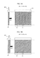
- FIG. 5A illustrates a condition of the surface of the crystalline silicon thin film when crystallized using a laser beam having an intensity distribution BP 1 with a full width at half maximum (FWHM) W 1 smaller than 20 ⁇ m in the manufacturing method for a bottom-gate semiconductor thin film device;
- FIG. 5B illustrates a condition of the surface of the crystalline silicon thin film when crystallized using a laser beam having an intensity distribution BP 1 with an FWHM of 20 ⁇ m or greater in the manufacturing method for a bottom-gate semiconductor thin film device;
- FIG. 6 illustrates cross-sectional views of the processes in the method of manufacturing a top-gate thin film semiconductor device according to the embodiment of the present invention
- FIG. 7 is a plan view schematically illustrating a thin film semiconductor array substrate according to the embodiment of the present invention.
- FIG. 8 is cross-sectional views (along A-A′ in FIG. 7 ) of processes in the manufacturing method for the thin film semiconductor array substrate according to the embodiment of the present invention.
- FIG. 9 illustrates a relationship between a surface temperature of a non-crystalline silicon thin film and time in the first thin film transistor (scanning direction SD 1 ) and the second thin film transistor (scanning direction SD 2 );
- FIG. 10A includes a plan view (a) and a cross-sectional view (b) illustrating the condition of crystals in the crystalline silicon thin film in the second thin film transistor (scanning direction SD 2 );
- FIG. 10B includes a plan view (a) and a cross-sectional view (b) illustrating the condition of crystals in the crystalline silicon thin film in the first thin film transistor (scanning direction SD 1 );
- FIG. 11 illustrates a relationship between a ratio of integral intensity values (S 2 /S 1 ) and a mobility ⁇ of the thin film transistor having the crystalline silicon thin film when the crystalline silicon thin film is formed with varying integral intensity values S 1 and S 2 in the CW laser beam illustrated in FIGS. 2A and 2B ;
- FIG. 12A indicates the intensity distribution BP 1 of the laser beam in the short-axis direction.
- FIG. 12B illustrates a relationship between a bottom-expansion starting value and the cooling time in the intensity distribution BP 1 of laser beam in the short-axis direction.
- An aspect of the manufacturing method for the thin film semiconductor device includes: preparing a substrate; forming a gate electrode above the substrate; forming a gate insulating film above the substrate; forming a source electrode and a drain electrode above the substrate; forming a silicon thin film above the substrate; and forming a crystalline silicon thin film by irradiating the silicon thin film with a laser beam while relatively scanning the silicon thin film with the laser beam in a predetermined relative scanning direction so as to crystallize the silicon thin film; wherein the laser beam is a continuous wave laser beam, an intensity distribution of the laser beam in a first region is symmetric on an anterior side and a posterior side of the relative scanning direction with a maximum intensity as a center, and the intensity distribution of the laser beam in a second region is asymmetric on the anterior side and the posterior side of the relative scanning direction with the maximum intensity as the center, the first region being a region from the maximum intensity of the laser beam to an intensity half of the maximum intensity, and the second region being a region equal to or lower
- the substrate preparation, the gate electrode formation, the gate insulating film formation, the silicon thin film formation, the crystalline silicon thin film formation, and the source and drain electrodes formation may be performed in this order, in the gate insulating film formation, the gate insulating film may be formed above the gate electrode, in the silicon thin film formation, the silicon thin film may be formed above the gate electrode and on the gate insulating film, and in the source and drain electrodes formation, the source electrode and the drain electrode may be formed above the crystalline silicon thin film.
- the substrate preparation, the silicon thin film formation, the crystalline silicon thin film formation, the gate insulating film formation, the gate electrode formation, and the source and drain electrodes formation may be performed in this order, in the gate insulating film formation, the gate insulating film may be formed above the crystalline silicon thin film, in the gate electrode formation, the gate electrode may be formed above the gate insulating film and in a region above the crystalline silicon thin film between the source electrode and the drain electrode, and in the source and drain electrodes formation, the source electrode and the drain electrode may be formed above the crystalline silicon thin film.
- a full width at half maximum (FWHM) of the intensity distribution of the laser beam is preferably between 20 and 50 ⁇ m inclusive.
- the integral intensity value S 1 and the integral intensity value S 2 are preferably calculated within a range from 3% to less than 50% of the maximum intensity of the intensity distribution of the laser beam, in the intensity distribution of the laser beam.
- the integral intensity value S 1 and the integral intensity value S 2 satisfy S 2 >1.5 ⁇ S 1 .
- the intensity distribution of the laser beam may be flat in a direction orthogonal to the relative scanning direction.
- a width of a flat part of the intensity distribution of the laser beam is preferably equal to or wider than a width of the silicon thin film in a direction orthogonal to the relative scanning direction.
- the crystalline silicon thin film may include a silicon crystal grain with a crystal grain size between 30 and 300 nm inclusive.
- the crystalline silicon thin film may be composed of silicon crystal grains each having a crystal grain size between 30 and 300 nm inclusive.
- the manufacturing method for the thin film semiconductor array substrate includes preparing a substrate; forming a gate electrode above the substrate; forming a gate insulating film above the substrate; forming a source electrode and a drain electrode above the substrate; forming a silicon thin film above the substrate; and forming a crystalline silicon thin film by irradiating the silicon thin film with a laser beam while relatively scanning the silicon thin film with the laser beam in a predetermined relative scanning direction so as to crystallize the silicon thin film, in which the laser beam is a continuous wave laser beam, an intensity distribution of the laser beam in a first region is symmetric on one side and the other side of the relative scanning direction with a maximum intensity as a center, and the intensity distribution of the laser beam in a second region is asymmetric on the one side and the other side of the relative scanning direction with the maximum intensity as the center, the first region being a region from the maximum intensity of the laser beam to an intensity half of the maximum intensity, and the second region being a region equal to or
- the substrate preparation, the gate electrode formation, the gate insulating film formation, the silicon thin film formation, the crystalline silicon thin film formation, and the source and drain electrodes formation may be performed in this order, in the gate insulating film formation, the gate insulating film may be formed above the gate electrode, in the silicon thin film formation, the silicon thin film may be formed above the gate electrode and on the gate insulating film, in the source and drain electrodes formation, the source electrode and the drain electrode may be formed above the crystalline silicon thin film.
- the substrate preparation, the silicon thin film formation, the crystalline silicon thin film formation, the gate insulating film formation, the gate electrode formation, and the source and drain electrodes formation may be performed in this order, in the gate insulating film formation, the gate insulating film may be formed above the crystalline silicon thin film, in the gate electrode formation, the gate electrode may be formed above the gate insulating film and in a region above the crystalline silicon thin film between the source electrode and the drain electrode, and in the source and drain electrodes formation, the source electrode and the drain electrode may be formed above the crystalline silicon thin film.
- a full width at half maximum (FWHM) of the intensity distribution of the laser beam is preferably between 20 to 50 ⁇ m inclusive.
- the integral intensity value S 1 and the integral intensity value S 2 preferably satisfy S 2 >1.5 ⁇ S 1 .
- an aspect of the method of forming the crystalline silicon thin film according to the present invention includes: preparing a substrate; forming a silicon thin film above the substrate; and forming a crystalline silicon thin film by irradiating the silicon thin film with a laser beam while relatively scanning the silicon thin film with the laser beam in a predetermined relative scanning direction so as to crystallize the silicon thin film, in which the laser beam is a continuous wave laser beam, an intensity distribution of the laser beam in a first region is symmetric on an anterior side and a posterior side of the relative scanning direction with a maximum intensity as a center, and the intensity distribution of the laser beam in a second region is asymmetric on the anterior side and the posterior side of the relative scanning direction with the maximum intensity as the center, the first region being a region from the maximum intensity of the laser beam to an intensity half of the maximum intensity, and the second region being a region equal to or lower than the half of the maximum intensity of the laser beam, and in the second region, an integral intensity value S 2 of the intensity distribution of the laser beam on the laser
- the crystalline silicon thin film with a large crystal grain size can be formed without changing the input energy.
- an aspect of the apparatus for forming the crystalline silicon thin film according to the present invention includes: a substrate holding unit which holds a substrate on which a silicon thin film is formed; a laser beam oscillating unit which oscillates a laser beam for crystallizing the silicon thin film; an optical system unit for irradiating a predetermined region of the silicon thin film with a laser beam oscillated from the laser beam oscillating unit; a scanning control unit for controlling the substrate holding unit and the optical system unit such that the silicon thin film is relatively scanned with the laser beam irradiated on the silicon thin film in a predetermined relative scanning direction; and a laser beam intensity distribution adjusting unit which shapes the laser beam such that an intensity distribution of the laser beam in a first region is symmetric on an anterior side and a posterior side of the relative scanning direction with a maximum intensity as a center, and the intensity distribution of the laser beam in a second region is asymmetric on the anterior side and the posterior side of the relative scanning direction with the maximum intensity as the center, the first region being a region
- a full width at half maximum (FWHM) of the intensity distribution of the laser beam is preferably between 20 to 50 ⁇ m inclusive.
- the integral intensity value S 1 and the integral intensity value S 2 preferably satisfy S 2 >1.5 ⁇ S 1 .
- an aspect of the apparatus for forming the crystalline silicon thin film according to the present invention may further include a laser beam inverting mechanism for inverting the intensity distribution of the laser beam such that the integral intensity value S 2 is the anterior side of the relative scanning direction, and the integral intensity value S 1 is the posterior side of the relative scanning direction.
- the optical system unit may include the laser beam inverting mechanism, and the optical system unit may invert the intensity distribution of the laser beam by outputting the laser beam in a non-inverted output or an inverted output.
- the substrate holding unit may include the laser beam inverting mechanism, and the substrate holding unit may invert the intensity distribution of the laser beam by rotating the substrate holding unit.
- FIG. 1 includes cross-sectional views of processes in the method of forming the crystalline silicon thin film according to the embodiment of the present invention.
- FIG. 2A illustrates an intensity distribution (beam profile) of CW laser beam used in a silicon thin film crystallizing process in the method of forming the crystalline silicon thin film according to the present invention.
- FIG. 2B illustrates an intensity distribution in the short-axis direction of the CW laser in FIG. 2A . Note that, in FIG. 2B , the intensity of the laser beam is normalized with the maximum intensity of the laser beam as 1.0.
- a substrate 10 is prepared (substrate preparation process).
- a non-crystalline silicon thin film 13 composed of an amorphous silicon film, for example, is formed above the substrate 10 (silicon thin film forming process).
- the silicon thin film 13 is irradiated with a laser beam, thereby crystallizing the silicon thin film 13 to form a crystalline silicon thin film 15 , as illustrated in FIG. 1 ( d ) (silicon thin film crystallizing process).
- the irradiation is performed along with a predetermined relative scanning direction with respect to the silicon thin film 13 , so as to perform relative scanning.
- the laser used in the embodiment is a continuous wave laser (CW laser). Unlike the pulse laser, the laser beam of the CW laser is continuously oscillated.
- the laser beam according to the embodiment has an intensity distribution BP 1 in the short-axis (x axis) direction, and an light intensity distribution BP 2 in the long axis (y axis) direction perpendicular to the short-axis direction.
- the intensity distribution BP 1 is a convex-shaped Gaussian distribution
- the light intensity distribution BP 2 is a top-flat distribution as illustrated in FIG. 2A .
- the intensity distribution BP 1 of the laser beam in the short-axis direction has the following characteristics.
- the intensity distribution is symmetric on the one side and the other side in the short-axis direction with the maximum intensity as the center.
- the intensity distribution is asymmetric with respect to the one side and the other side in the short-axis direction.
- the intensity distribution of the laser beam in the short-axis direction is shaped as follows.
- the integral intensity value S 2 of the intensity distribution of the laser beam on the other side with the maximum intensity as the center (the area indicated by the right-downward diagonal hatching) is formed to be larger than the integral intensity value S 1 of the intensity distribution of the laser beam on one side with the maximum intensity as the center (the area indicated by the right-upward diagonal hatching).
- the relationship between the integral intensity value S 2 and the integral intensity value S 1 is S 2 >S 1 .
- W 1 represents a full width at half maximum (FWHM) of the intensity distribution BP 1 in the short-axis direction of the laser beam.
- W 2 represents a long axis-wise width of the intensity distribution BP 2 in the long-axis direction of the laser beam (flat width).
- the non-crystalline silicon thin film is irradiated with the laser beam with the scanning direction SD 1 on the anterior side (heat input side) and with the scanning direction SD 2 on the posterior side (cooling side). More specifically, the relative scanning of the laser beam is performed with the light intensity distribution forming the integral intensity value S 1 on the anterior side of the relative scanning direction, and with the light intensity distribution forming the integral intensity value S 2 on the posterior side of the relative scanning direction. Note that, in FIGS. 2A and 2B , the scanning direction SD 1 and the scanning direction SD 2 represent scanning directions that are opposite to each other.
- the intensity distribution of the CW laser beam when crystallizing the silicon thin film is configured such that the integral intensity value S 2 in the posterior side of the beam scanning direction (cooling side) is larger than the anterior side of the beam scanning direction (heat input side). More specifically, the intensity distribution of the laser beam in the embodiment is asymmetric on the heat input side and the cooling side, and has an expanded bottom on the cooling side.
- the crystalline silicon thin film with a large crystal grain size can be formed without changing the input energy determined by the FWHM.
- FIG. 3 illustrates the configuration of the crystalline silicon thin film forming apparatus according to the embodiment of the present invention.
- the crystalline silicon thin film forming apparatus 100 is an apparatus using the CW laser beam for crystallizing the silicon thin film, and includes a substrate holding unit 110 , a laser beam oscillating unit 120 , a optical system unit 130 , and a control unit 140 including a scanning control unit 141 and the laser beam intensity distribution adjusting unit 142 .
- the laser beam oscillating unit 120 is an optical source for oscillating the laser beam LB for crystallizing the silicon thin film.
- Four semiconductor laser devices are provided in the laser beam oscillating unit 120 , and each of the semiconductor laser devices oscillates a laser beam having single-peaked bilaterally symmetric light intensity distribution.
- a blue laser beam or a green laser beam with a wavelength range between 405 nm and 632 nm is continuously oscillated in the micro second order of 10 to 100 ⁇ secs, for example.
- the optical system unit 130 includes beam-shaping lenses, and is configured to shape the laser beam LB oscillated by the laser beam oscillating unit 120 into a predetermined intensity distribution, and to irradiate a predetermined region of the silicon thin film with the laser beam LB.
- the optical system unit 130 is configured of a homogenizer 131 , a condenser lens 132 , and a diffractive optical element (DOE) lens 133 .
- DOE diffractive optical element
- the laser beam intensity distribution adjusting unit 142 shapes the laser beam LB to have the predetermined intensity distribution.
- the laser beam intensity distribution adjusting unit 142 shapes the laser beam LB oscillated by the laser beam oscillating unit 120 by adjusting the lenses configuring the optical system unit 130 , and by shaping the laser beam LB to have the light intensity distribution illustrated in FIGS. 2A and 2B .
- the crystalline silicon thin film forming apparatus 100 may further include optical parts such as a mirror and a light-condensing lens, or may also include a beam profiler for measuring the beam profile of the laser beam. Measuring the beam profile by the beam profiler allows adjusting the position of the lenses in the optical system 130 by the laser beam intensity distribution adjusting unit 142 such that the laser beam used for irradiation on the silicon thin film has the desired light intensity distribution, for example.
- the manufacturing method for the thin film semiconductor device includes a process for preparing the substrate (substrate preparation process), a process for forming the gate electrode above the substrate (gate electrode forming process), a process for forming the gate insulating film above the substrate (gate insulating film forming process), a process for forming the source electrode and the drain electrode above the substrate (source/drain electrode forming process), a process for forming a silicon thin film above the substrate (silicon thin film forming process), and a process for forming a crystalline silicon thin film by irradiating the laser beam so as to crystallize the silicon thin film formed above the substrate (silicon thin film crystallizing process).
- the thin film semiconductor device has two types of structures, i.e., the bottom-gate type and the top-gate type.
- the bottom-gate thin film semiconductor device is layered, from the bottom, the gate electrode, the gate insulating film, and the channel layer (silicon semiconductor film).
- the top-gate thin film semiconductor device is layered, from the bottom, the channel layer, the gate insulating film, and the gate electrode. The following shall specifically describe the manufacturing method for the bottom-gate and top-gate thin film semiconductor devices with reference to the drawings.
- a substrate 10 is prepared (substrate preparation process).
- a glass substrate may be used as the substrate 10 , for example.
- an undercoating film composed of an insulating film such as a silicon oxide film or a silicon nitride film may be subsequently formed on the substrate 10 .
- the crystalline silicon thin film 15 is formed by irradiating the predetermined region of the silicon thin film 13 with the laser beam while relatively scanning the silicon thin film 13 with the laser beam so as to crystallize the silicon thin film 13 (silicon thin film crystallizing process). This process is performed in a method similar to the silicon thin film crystallizing process in the method of forming the crystalline silicon thin film described above.
- the relative scanning of the laser beam is performed with the relative scanning direction on the short-axis direction of the intensity distribution of the laser beam, the light intensity distribution composing the integral intensity value S 1 being the anterior side of the relative scanning direction, and the light intensity distribution composing the integral intensity value S 2 being the posterior side of the relative scanning direction.
- the silicon thin film irradiated with the laser beam is heated and crystallized, turning to the crystalline silicon thin film 15 .
- the crystalline silicon thin film 15 is patterned into an island shape by performing photolithography and wet etching so as to selectively pattern the non-crystalline silicon thin film 13 and the crystalline silicon thin film 15 .
- the contact layer 17 is separated, and a pair of opposing contact layers 17 is formed. With this, as illustrated in FIG. 4 ( g ), the bottom-gate thin film semiconductor device is manufactured.
- the intensity distribution of the CW laser beam for crystallizing the silicon thin film to be the channel layer is configured such that the integral intensity value S 2 of the light intensity distribution in the posterior side (cooling side) of the beam scanning direction is larger than the integral intensity value S 1 of the light intensity distribution in the anterior side (heat input side) of the beam scanning direction.
- the intensity distribution of the laser beam in the embodiment is asymmetric on the heat input side and the cooling side, and has an expanded bottom on the cooling side.
- the laser beam with the intensity distribution illustrated in FIGS. 2A and 2B is used. It is preferable that the FWHM W 1 of the intensity distribution BP 1 of the laser beam in the short-axis direction is between 20 and 50 ⁇ m. This point shall be described with reference to FIGS. 5A and 5B .
- FIG. 5A illustrates a condition of the surface of the crystalline silicon thin film when the crystalline silicon thin film is crystallized by the laser beam with the intensity distribution BP 1 with the FWHM W 1 smaller than 20 ⁇ m in the manufacturing method for the bottom-gate semiconductor thin film device.
- FIG. 5B illustrates a condition of the surface of the crystalline silicon thin film when crystallized by the laser beam with the intensity distribution BP 1 with the FWHM equal to or wider than 20 ⁇ m.
- the laser irradiation is performed with the scanning direction SD 1 illustrated in FIGS. 2A and 2B as the scanning direction such that the heat input side is the integral intensity value S 1 and the cooling side is the integral intensity value S 2 .
- the FWHM of the intensity distribution BP 1 of the laser beam exceeds 50 ⁇ m results in a decrease in the energy efficiency of the laser beam.
- the crystalline silicon thin film formed in the silicon thin film crystallizing process includes silicon crystal grains with the crystal grain size between 30 and 300 nm.
- the silicon thin film at the time of crystallization is within a temperature range lower than the melting point of the amorphous silicon film referred to as the solid phase crystallization (SPC) (between 600° C. and 1100° C.) (between 600° C. and 1100° C.)
- the silicon thin film is crystallized by the solid phase growth, changing to the crystalline silicon thin film with a crystal structure having an average crystal grain size approximately between 25 nm and 35 nm.
- the temperature of the silicon thin film at the time of crystallization is a temperature range equal to or higher than the melting point of the amorphous silicon and equal to or less then the melting point of silicon referred to as explosive nucleation (Ex) (between 1100° C. and 1414° C.)
- the silicon thin film is crystallized after going through supercooled liquid state, changing to the crystalline silicon thin film with crystal structure having an average crystal grain size between 40 nm and 60 nm.
- the silicon thin film at the time of crystallization is within a temperature range equal to or higher than the melting point of silicon referred to as the molten range (1414° C. or higher)
- the silicon thin film is crystallized after being melt and cooled, changing to the crystalline silicon thin film composed of polysilicon having the crystal structure with an average grain size between 60 nm and 1 ⁇ m.
- the silicon thin film crystallizing process it is possible to form the crystalline silicon thin film at least with silicon crystal grains with the crystal grain size between 30 and 300 nm. Furthermore, according to the embodiment, it is possible to form the mixed crystal crystalline silicon thin film including silicon crystal grains having a crystal grain size between 30 and 300 nm, or to form the crystalline silicon thin film with all of the silicon crystal grains having the crystal grain size between 30 and 300 nm.
- FIG. 6 includes cross-sectional views illustrating processes of the manufacturing method for the top-gate thin film semiconductor device according to the embodiment of the present invention.
- a substrate 10 is prepared (substrate preparation process).
- a glass substrate may be used as the substrate 10 , for example.
- the undercoating film 21 made of a silicon oxide film or a silicon nitride film is formed on the substrate 10 .
- the non-crystalline silicon thin film 13 is formed above the substrate 10 (silicon thin film forming process).
- the amorphous silicon film is formed by plasma CVD, for example, as the non-crystalline silicon thin film 13 .
- the crystalline silicon thin film 15 is formed by irradiating the predetermined region of the silicon thin film 13 with the laser beam while relatively scanning the silicon thin film 13 with the laser beam so as to crystallize the silicon thin film 13 (silicon thin film crystallizing process).
- This process is performed in the same manner as the silicon thin film crystallizing process in the method of forming the crystalline silicon thin film, that is, in the same manner as the silicon thin film crystallizing process in the manufacturing method for the bottom-gate thin film semiconductor device as illustrated in FIG. 4 ( e ).
- the silicon thin film 13 is irradiated with the CW laser beam with the light intensity distribution illustrated in FIGS. 2A and 2B in a microsecond order. Furthermore, the irradiation with the laser beam is performed such that the laser scanning is performed toward the depth direction of the sheet of FIG. 6 . More specifically, among the scanning direction SD 1 and the scanning direction SD 2 illustrated in FIGS. 2A and 2B , the irradiation is performed with the scanning direction SD 1 on the anterior side (heat input side) and with the scanning direction SD 2 on the posterior side (cooling side).
- the relative scanning of the laser beam is performed with the relative scanning direction on the short-axis direction of the intensity distribution of the laser beam, the light intensity distribution composing the integral intensity value S 1 being the anterior side of the relative scanning direction, and the light intensity distribution composing the integral intensity value S 2 being the posterior side of the relative scanning direction.
- the silicon thin film which is irradiated with the laser beam is heated and crystallized, turning to the crystalline silicon thin film 15 .
- the photolithography and wet etching are performed so as to selectively pattern the non-crystalline silicon thin film 13 and the crystalline silicon thin film 15 and to pattern the crystalline silicon thin film 15 into an island shape.
- the gate insulating film 12 is formed above the substrate 10 (gate insulating film forming process).
- the gate insulating film 12 made of an insulating film such as silicon dioxide is formed on the entire surface above the substrate 10 covering the gate electrode 15 by plasma CVD, for example.
- the gate electrode 11 is formed above the substrate 10 by patterning (gate electrode forming process).
- the gate metal film such as molybdenum-tungsten (MoW) is formed by sputtering on the entire surface above the substrate 10 , and the gate metal film is patterned by performing photolithography and wet etching, and thus the gate electrode 11 of the predetermined shape is formed above the crystalline silicon thin film 15 via the gate insulating film 12 .
- the lightly doped drain (LDD) region 22 is formed by lightly doping impurity at the ends of the crystalline silicon thin film 15 using the gate electrode 11 as a mask.
- the passivation film 23 is formed above the substrate 10 .
- the passivation film 23 composed of an insulating film such as silicon dioxide is formed on the entire surface above the substrate 10 by plasma CVD, for example, covering the gate electrode 11 and the gate insulating film 12 .
- contact holes are formed on the passivation film 23 , exposing the LDD region 22 .
- the intensity distribution of the CW laser beam for crystallizing the silicon thin film to be the channel layer is configured in the same manner as in the manufacturing method for the bottom-gate thin film semiconductor device such that the integral intensity value S 2 of the light intensity distribution on the posterior side (cooling side) of the beam scanning direction is larger than the integral intensity value S 1 of the light intensity distribution on the anterior side (heat input side) of the beam scanning direction.
- the FWHM W 1 of the intensity distribution BP 1 of the laser beam in the short-axis direction is between 20 and 50 ⁇ m, in the same manner as in the bottom-gate thin film semiconductor device.
- the flat width in the intensity distribution BP 2 of the laser beam in the Y-axis direction is equal to or wider than the width of the silicon thin film 13 in a portion of the silicon thin film 13 to be the channel layer (the width of the silicon thin film in a direction orthogonal to the relative scanning direction).
- the top-gate thin film semiconductor device it is possible to form a crystalline silicon thin film at least with silicon crystal grains having crystal grain size between 30 and 300 nm, and to form a crystalline silicon thin film with all of the silicon crystal grains having a crystal grain size between 30 and 300 nm.
- FIG. 7 is a plan view schematically illustrating the thin film semiconductor array substrate according to the embodiment of the present invention.
- FIG. 8 illustrates cross-sectional views of the processes in the manufacturing method for the thin film semiconductor array substrate according to the embodiment of the present invention, and the cross-sectional views are along the line A-A′ in FIG. 7 . Note that, in the manufacturing method of the thin film semiconductor array substrate, formation of the bottom-gate thin film semiconductor device shall be described. The manufacturing method is also applicable to the top-gate thin film semiconductor device.
- the thin film semiconductor array substrate is a TFT array substrate in which thin film transistors (thin film semiconductor devices) are formed, and includes multiple pixels arranged in a matrix. Each of the pixels are partitioned by the gate line arranged in the row direction and the source line arranged in the column direction, and one pixel (unit pixel) includes a driving transistor DTr and a switching transistor STr.
- the organic EL element is formed on the thin film semiconductor array substrate.
- the driving transistor DTr is a thin film transistor for driving the organic EL element
- the switching transistor STr serves as a thin film transistor for supplying a video signal from the source line to the pixel.
- the substrate 10 is prepared as illustrated in FIG. 7 ( a ) (substrate preparation process).
- a glass substrate may be used as the substrate 10 , for example.
- an undercoating film may be formed on the substrate 10 .
- a first gate electrode 11 a of the driving transistor DTr and a second gate electrode 11 b of the switching transistor STr are formed by patterning above the substrate 10 (gate electrode forming process).
- a gate metal film such as molybdenum-tungsten (MoW) is formed by sputtering on the entire surface above the substrate 10 , and photolithography and wet etching are performed on the gate metal film so as to pattern the first gate electrode 11 a and the second gate electrode 11 b in the predetermined shape.
- the gate insulating film 12 is formed above the substrate 10 (gate insulating film forming process).
- the gate insulating film 12 composed of an insulating film such as silicon dioxide is firmed on the entire surface above the substrate 10 by plasma CVD, for example, so as to cover the first gate electrode 11 a and the second gate electrode 11 b.
- the silicon thin film 13 is crystallized by relatively scanning the silicon thin film 13 with the laser beam so as to irradiate the predetermined region of the silicon thin film corresponding to the channel layer of the driving transistor DTr with the laser beam, so as to form the crystalline silicon thin film (the first crystalline silicon thin film) 15 (first silicon thin film crystallizing process).
- the silicon thin film 13 is irradiated with the CW laser beam with the light intensity distribution illustrated in FIGS. 2A and 2B in a microsecond order. Furthermore, the laser beam irradiation is performed toward the depth direction of the sheet of FIG. 7 . More specifically, among the scanning direction SD 1 and the scanning direction SD 2 illustrated in FIGS. 2A and 2B , the irradiation is performed with the scanning direction SD 1 on the anterior side (heat input side) and with the scanning direction SD 2 on the posterior side (cooling side).
- the relative scanning using the laser beam is performed with the relative scanning direction on the short-axis direction of the intensity distribution of the laser beam, the light intensity distribution composing the integral intensity value S 1 being the anterior side of the relative scanning direction, and the light intensity distribution composing the integral intensity value S 2 being the posterior side of the relative scanning direction.
- the laser beam is irradiated along the row direction from a scanning starting end of the laser beam which is one end of the substrate in the row direction to a scanning end which is the other end of the substrate.
- the silicon thin film in a part on which the laser beam is irradiated is sequentially heated and crystallized, forming a band-shaped crystalline silicon thin film 15 .
- the predetermined region of the silicon thin film 13 corresponding to the channel layer of the switching transistor STr is irradiated, thereby crystallizing the silicon thin film 13 so as to form the crystalline silicon thin film (the second crystalline silicon thin film) 16 (second silicon thin film crystallizing process).
- the intensity distribution of the laser beam with respect to the scanning direction is inverted such that the integral intensity value of the intensity distribution of the laser beam on the cooling side of the scanning direction is larger than the integral intensity value of the intensity distribution of the laser beam on the heat input side of the scanning direction.
- the laser irradiation is performed using the CW laser beam having the light intensity distribution illustrated in FIGS. 2A and 2B .
- the laser beam irradiation is performed with the scanning direction SD 2 on the anterior side (heat input side) and the scanning direction SD 1 on the posterior side (cooling side) such that the laser scanning is performed toward the forward direction of the sheet of FIG. 8 .
- the relative scanning of the laser beam is performed with the relative scanning direction on the short-axis direction of the intensity distribution of the laser beam, the light intensity distribution composing the integral intensity value S 2 being the anterior side of the relative scanning direction, and the light intensity distribution composing the integral intensity value S 1 being the posterior side of the relative scanning direction.
- the laser irradiation is performed to the scanning end which is the other end of the substrate in the row direction as described above, and subsequently, another scanning is started with the scanning end as a new scanning starting end, and the laser irradiation is performed along the row direction from the scanning staring end of the laser beam which is the other end of the substrate in the row direction to the scanning end which is the one end of the substrate in the row direction.
- the silicon thin film on which the laser beam is irradiated is sequentially heated and crystallized, forming a band-shaped crystalline silicon thin film 16 .
- the crystalline silicon thin film corresponding to the channel layer for all of the pixels on the substrate is formed by alternately repeating the first silicon thin film crystallizing process and the second thin film crystallizing process in the column direction.
- the first silicon thin film crystallizing process is a laser scanning from the end of the substrate to the other end of the substrate in the row direction
- the second silicon thin film crystallizing process is a laser scanning from the other end of the substrate to the one end of the substrate in the row direction.
- the non-crystalline silicon thin film 13 and the crystalline silicon thin films 15 and 16 are selectively patterned, forming the crystalline silicon thin films 15 and 16 in island pattern in each pixel.
- the amorphous silicon film is formed by plasma CVD, for example, and impurity such as phosphorous is doped on the amorphous silicon film to form an impurity doped n + layer is formed to be the contact layer 17 .
- impurity such as phosphorous
- n + layer is formed to be the contact layer 17 .
- a pair of the first source electrode 19 a and the first drain electrode 20 a , and a pair of the second source electrode 19 b and the second drain electrode 20 b are formed above the substrate 10 (source/drain electrodes forming process). For example, photolithography and wet etching are performed so as to pattern the source/drain metal film 18 such that the first source electrode 19 a and the first drain electrode 20 a , and the second source electrode 19 b and the second drain electrode 20 b are formed.
- the contact layer 17 is separated, and a pair of opposing contact layers 17 is formed.
- the thin film semiconductor array substrate according to the embodiment of the present invention including the driving transistor DTr and the switching transistor STr are manufactured.
- the intensity distribution of the CW laser beam when crystallizing the silicon thin film to be the channel layer of the driving transistor DTr is configured such that the integral intensity distribution value S 2 of the light intensity distribution on the posterior side of the beam scanning direction (cooling side) is larger than the integral intensity value S 1 of the light intensity distribution in the anterior side of the beam scanning direction (heat input side). More specifically, the intensity distribution is asymmetrical on the heat input side and the cooling side, and has an expanded bottom on the cooling side.
- the intensity distribution of the CW laser beam when crystallizing the silicon thin film to be the channel layer of the switching transistor STr has the same light intensity distribution as the CW laser beam when crystallizing the silicon thin film in the driving transistor DTr.
- the beam scanning direction is inverted such that the integral intensity value S 2 of the light intensity distribution on the anterior side of the beam scanning direction (heat input side) is greater than the integral intensity value S 1 in the posterior side of the beam scanning direction (cooling side). More specifically, the intensity distribution is configured such that the heat input side has an expanded bottom.
- the silicon thin film corresponding to the driving transistor DTr is scanned with the laser beam in the direction of the scanning direction SD 1 as illustrated in FIGS. 2A and 2B
- the silicon thin film corresponding to the switching transistor STr is scanned with the laser beam in the direction of the scanning direction SD 2 as illustrated in FIGS. 2A and 2B .
- the cooling speed for the silicon thin film corresponding to the switching transistor STr is not slowed down.
- the manufacturing method for the thin film semiconductor array substrate using different scanning directions of the CW laser beam with the intensity distribution illustrated in FIGS. 2A and 2B , it is possible to easily form the crystalline silicon thin films with different crystal states (crystal grain sizes) without changing the output waveform of the laser. Therefore, the thin film semiconductor array substrate including thin film semiconductor devices with different TFT characteristics can be easily manufactured.
- the beam scanning direction may be inverted using the crystalline silicon thin film forming apparatus 100 illustrated in FIG. 3 .
- the crystalline silicon thin film forming apparatus 100 includes a laser beam inversion mechanism for inverting the beam scanning direction such that the intensity distribution of the laser beam with respect to the silicon thin film is inverted.
- the optical system unit 130 illustrated in FIG. 3 may include the laser beam inversion mechanism.
- the optical system unit 130 is configured to output non-inverted or inverted laser beam, and the intensity distribution of the laser beam can be inverted by outputting non-inverted or inverted laser beam by the optical system unit 130 .
- the substrate holding unit 110 illustrated in FIG. 3 may include the laser beam inversion mechanism.
- a driving mechanism capable of changing the orientation by 180 degrees is included in the substrate holding unit 110 , and the intensity distribution of the laser beam may be inverted by rotating the substrate holding unit 110 by 180 degrees.
- the first and second thin film transistors in a case in which the crystalline silicon thin films are formed by inverting the scanning directions of the laser beam using the CW laser beam having the intensity distribution illustrated in FIGS. 2A and 2B are manufactured.
- the first and second thin film transistors shall be described.
- the first thin film transistor includes the crystalline silicon thin film 15 crystallized by scanning with the laser beam in the scanning direction SD 1 with the expanded bottom (the integral intensity value S 2 ) on the cooling side in FIGS. 2A and 2B .
- the second thin film transistor includes the crystalline silicon thin film 16 crystallized by scanning with the laser beam in the scanning direction SD 2 with the expanded bottom on the heat input side.
- the first thin film transistor and the second thin film transistor correspond to the driving transistor DTr and the switching transistor STr, respectively.
- FIG. 9 illustrates the relationship between surface temperature and time of the non-crystalline silicon thin film in the first thin film transistor (scanning direction SD 1 ) and the second thin film transistor (scanning direction SD 2 ).
- the first thin film transistor with the crystalline silicon thin film crystallized by the scanning with the laser beam having the expanded bottom on the cooling side can slow down the cooling speed, compared to the second thin film transistor with the crystalline silicon thin film crystallized by the scanning with the laser beam in the opposite direction. It is assumed that this makes the crystal grain size of the crystalline silicon thin film for the first thin film transistor greater than the crystal grain size of the crystalline silicon thin film for the second thin film transistor.
- FIG. 10A includes a plan view (a) and a cross-sectional view (b) illustrating the crystal state of the crystalline silicon thin film in the second thin film transistor (the scanning direction SD 2 ).
- FIG. 10B includes a plan view (a) and a cross-sectional view (b) illustrating the crystal state of the crystalline silicon thin film in the first thin film transistor (the scanning direction SD 1 ).
- the crystalline silicon thin film 16 in the second thin film transistor is formed with a plurality of crystal grains (crystal particles) 16 a with a crystal grain size 16 c , and the boundary of the crystal grains 16 a forms a crystal grain boundary 16 b .
- the crystalline silicon thin film 15 in the first thin film transistor is formed with multiple crystal grains (crystal particles) 15 a with a crystal grain size 15 c , and the boundary of the crystal grains 15 a forms a crystal grain boundary 15 b.
- the electron (e) passes multiple crystal grains 15 a ( 16 a )
- the electron passes through the crystal grain boundaries 15 b ( 16 b )
- the number of crystal grain boundaries 15 b ( 16 b ) is in proportion to the number of crystal grains 15 a ( 16 a ). Since the grain boundary 15 b ( 16 b ) is a crystal defect, the electron (e) tends to be trapped at the grain boundary 15 b ( 16 b ). Accordingly, the larger the crystal grain size 15 c ( 16 c ) becomes, the smaller the number of the crystal grain boundaries 15 b ( 16 b ) becomes, decreasing the probability of the electron (e) trapped and increasing the mobility of the electron (e).
- the mechanism of the crystal growth of the amorphous silicon film is as follows: first, a crystal nucleus is formed, and the crystal grows from the crystal nucleus. More specifically, in the solid-phase growth of the silicon thin film, the crystal nuclei are formed in the amorphous silicon film as the activation energy (free energy) increases, and crystals grow from the crystal nuclei.
- the crystal grain size g may be represented by the following equation using the activation energy En for generating the crystal nuclei of silicon and the activation energy Eg of the crystal growth speed. Note that, k denotes the Boltzmann coefficient, and T denotes absolute temperature. g ⁇ exp[( En ⁇ Eg )/3 kT]
- the crystal grain size g increases and the thermal processing time significantly increases as the thermal processing temperature is decreased, and thus, it is assumed that the crystal grain size g increases as the thermal processing time increases. Therefore, it is possible to increase the crystal grain size g by increasing the cooling time for molten silicon, and with this, the crystal grain boundary is decreased, increasing the mobility of the electron.
- the number of crystal grain boundary is smaller and the crystal grain size is smaller in the crystalline silicon thin film 15 in the second thin film transistor than in the crystalline silicon thin film 16 in the first thin film transistor.
- the mobility of the electron (e) is larger in the case where the electron (e) moves in the crystalline silicon thin film 15 in the second thin film transistor as illustrated in FIG. 10B than in the case where the electron (e) moves in the crystalline silicon thin film 16 in the first thin film transistor as illustrated in FIG. 10A .
- the electron mobility of the first thin film transistor and the second thin film transistor that are actually manufactured is measured.
- the mobility ⁇ of the first thin film transistor is 28.7 (cm 2 /V ⁇ sec) and the mobility ⁇ of the second thin film transistor is 23.7 (cm 2 /V ⁇ sec). Accordingly, the mobility in the first thin film transistor is larger than the mobility in the second thin film transistor.
- the output of the laser beam is 80 (kW/cm 2 ), and the scanning speed of the laser is 380 (mm/s).
- FIG. 11 is a graph illustrating a relationship between a ratio of integral intensity values (S 2 /S 1 ) and the mobility g of the thin film transistor having the crystalline silicon thin film when the crystalline silicon thin film is formed with varying the integral intensity values S 1 and S 2 in the CW laser beam illustrated in FIGS. 2A and 2B .
- the bottom expansion starting value X needs to be 3.0% or higher in order to increase the cooling time for crystallizing the silicon thin film by 10%.
- the bottom expansion starting value X in order to maintain the input energy (energy density) determined by the FWHM W 1 at the same level, it is necessary to set the bottom expansion starting value X at 50.0% or lower. Therefore, it is preferable to set the bottom expansion starting value X (%) on the cooling side between 3.0% and 50%.
- the manufacturing method for thin film semiconductor device, the manufacturing method for the thin film semiconductor array substrate, the method of forming crystalline silicon thin film, and the apparatus for forming the crystalline silicon thin film according to the present invention have been described based on the embodiment. However, the present invention is not limited to the embodiment described above.
- the thin film semiconductor device or the thin film semiconductor array substrate manufactured according to the embodiment may be used for a display apparatus such as an organic EL display apparatus or a liquid crystal display.
- the display apparatus may be used as a flat panel display, and may be applicable to an electronic device such as a television set, a personal computer, or a mobile phone.
- the crystalline silicon thin film manufactured based on the embodiment may be used not only for the thin film semiconductor device but also for an electronic device such as a solar cell or a sensor.
Landscapes
- Recrystallisation Techniques (AREA)
- Thin Film Transistor (AREA)
- Metal-Oxide And Bipolar Metal-Oxide Semiconductor Integrated Circuits (AREA)
Abstract
Description
g∝exp[(En−Eg)/3kT]
Claims (17)
Applications Claiming Priority (1)
| Application Number | Priority Date | Filing Date | Title |
|---|---|---|---|
| PCT/JP2011/003109 WO2012164626A1 (en) | 2011-06-02 | 2011-06-02 | Thin film semiconductor device manufacturing method, thin film semiconductor array substrate manufacturing method, crystal silicon thin film forming method, and crystal silicon thin film forming device |
Related Parent Applications (1)
| Application Number | Title | Priority Date | Filing Date |
|---|---|---|---|
| PCT/JP2011/003109 Continuation WO2012164626A1 (en) | 2011-06-02 | 2011-06-02 | Thin film semiconductor device manufacturing method, thin film semiconductor array substrate manufacturing method, crystal silicon thin film forming method, and crystal silicon thin film forming device |
Publications (2)
| Publication Number | Publication Date |
|---|---|
| US20120309140A1 US20120309140A1 (en) | 2012-12-06 |
| US8735233B2 true US8735233B2 (en) | 2014-05-27 |
Family
ID=47258518
Family Applications (1)
| Application Number | Title | Priority Date | Filing Date |
|---|---|---|---|
| US13/451,078 Expired - Fee Related US8735233B2 (en) | 2011-06-02 | 2012-04-19 | Manufacturing method for thin film semiconductor device, manufacturing method for thin film semiconductor array substrate, method of forming crystalline silicon thin film, and apparatus for forming crystalline silicon thin film |
Country Status (5)
| Country | Link |
|---|---|
| US (1) | US8735233B2 (en) |
| JP (1) | JPWO2012164626A1 (en) |
| KR (1) | KR20140018081A (en) |
| CN (1) | CN103003928A (en) |
| WO (1) | WO2012164626A1 (en) |
Cited By (3)
| Publication number | Priority date | Publication date | Assignee | Title |
|---|---|---|---|---|
| US20140231813A1 (en) * | 2011-10-03 | 2014-08-21 | Panasonic Corporation | Thin-film device, thin-film device array, and method of manufacturing thin-film device |
| US9236254B2 (en) | 2011-11-09 | 2016-01-12 | Joled Inc. | Substrate having thin film and method of thin film formation |
| US12176353B2 (en) | 2020-03-02 | 2024-12-24 | Adrc. Co. Kr | Thin film transistor including crystallized semiconductor, display device including the same, manufacturing method of the same, and method for crystallizing semiconductor |
Families Citing this family (6)
| Publication number | Priority date | Publication date | Assignee | Title |
|---|---|---|---|---|
| JP5508535B2 (en) | 2011-03-22 | 2014-06-04 | パナソニック株式会社 | Semiconductor thin film forming method, semiconductor device, semiconductor device manufacturing method, substrate, and thin film substrate |
| WO2013031198A1 (en) | 2011-08-30 | 2013-03-07 | パナソニック株式会社 | Method for manufacturing thin-film-formation substrate, method for manufacturing thin-film-element substrate, thin-film substrate, and thin-film-element substrate |
| KR102235601B1 (en) * | 2014-05-29 | 2021-04-05 | 삼성디스플레이 주식회사 | Active layer of thin film transistor crystallizing apparatus and the crystallizing method using the same |
| WO2017145330A1 (en) * | 2016-02-25 | 2017-08-31 | 株式会社島津製作所 | Laser processing device |
| JP6985711B2 (en) * | 2017-02-28 | 2021-12-22 | 国立大学法人 筑波大学 | Manufacturing method of semiconductor device |
| WO2019075454A1 (en) * | 2017-10-13 | 2019-04-18 | The Trustees Of Columbia University In The City Of New York | Systems and methods for spot beam and line beam crystallization |
Citations (25)
| Publication number | Priority date | Publication date | Assignee | Title |
|---|---|---|---|---|
| US4679184A (en) * | 1984-06-08 | 1987-07-07 | Matsushita Electric Industrial Co., Ltd. | Optical recording and reproducing apparatus having erasing beam spot with asymmetrical intensity distribution |
| JPH07235490A (en) | 1994-02-23 | 1995-09-05 | Sony Corp | Method for forming polycrystalline silicon thin film and method for forming channel of MOS transistor |
| US5529951A (en) | 1993-11-02 | 1996-06-25 | Sony Corporation | Method of forming polycrystalline silicon layer on substrate by large area excimer laser irradiation |
| US20040074881A1 (en) | 2002-10-16 | 2004-04-22 | Semiconductor Energy Laboratory Co., Ltd. | Laser irradiation apparatus and method of manufacturing semiconductor device by using the laser irradiation apparatus |
| JP2004158837A (en) | 2002-10-16 | 2004-06-03 | Semiconductor Energy Lab Co Ltd | Laser irradiation apparatus and method for manufacturing semiconductor device using laser irradiation apparatus |
| JP2004260144A (en) * | 2003-02-06 | 2004-09-16 | Mitsubishi Electric Corp | Laser annealing method and apparatus |
| US6863733B1 (en) * | 1999-07-15 | 2005-03-08 | Nec Corporation | Apparatus for fabricating thin-film semiconductor device |
| US20050236622A1 (en) | 2004-04-08 | 2005-10-27 | Samsung Electronics Co., Ltd. | Electronic device and method of manufacturing the same |
| US20070070283A1 (en) * | 2005-09-26 | 2007-03-29 | Masahiro Maki | Display Device |
| US20070148834A1 (en) * | 2004-06-18 | 2007-06-28 | Semiconductor Energy Laboratory Co., Ltd. | Laser irradiation apparatus and laser irradiation method |
| JP2007221062A (en) | 2006-02-20 | 2007-08-30 | Sharp Corp | Semiconductor device manufacturing method and manufacturing apparatus |
| US20080035926A1 (en) * | 2006-08-08 | 2008-02-14 | Sony Corporation | Display device and display device manufacturing method |
| JP2008091811A (en) | 2006-10-05 | 2008-04-17 | Ihi Corp | Laser annealing method and laser annealer |
| US20080171410A1 (en) * | 2006-08-31 | 2008-07-17 | Semiconductor Energy Laboratory Co., Ltd. | Method for manufacturing crystalline semiconductor film and semiconductor device |
| JP2008305866A (en) | 2007-06-05 | 2008-12-18 | Hitachi Displays Ltd | Manufacturing method of image display device |
| US20090046757A1 (en) * | 2007-08-16 | 2009-02-19 | Semiconductor Energy Laboratory Co., Ltd. | Laser irradiation apparatus, laser irradiation method, and manufacturing method of semiconductor device |
| US7502107B2 (en) * | 2003-08-22 | 2009-03-10 | Secretary, Department Of Atomic Energy, Government Of India | Apparatus and method for transport of microscopic object(s) |
| US20090269893A1 (en) * | 2001-07-05 | 2009-10-29 | Fujitsu Limited | Semiconductor integrated circuit device and method of producing the same |
| JP2010153876A (en) | 2010-01-08 | 2010-07-08 | Hitachi Displays Ltd | Method for reforming semiconductor thin film, reformed semiconductor thin film, method for evaluating reformed semiconductor thin film, thin film transistor formed of the semiconductor thin film, and image display device with circuit constituted using the thin film transistor |
| US20100207040A1 (en) * | 2004-12-24 | 2010-08-19 | Semiconductor Energy Laboratory Co., Ltd. | Light exposure apparatus and manufacturing method of semiconductor device using the same |
| US20110297950A1 (en) | 2010-05-10 | 2011-12-08 | Panasonic Liquid Crystal Display Co., Ltd. | Crystalline semiconductor film manufacturing method, substrate coated with crystalline semiconductor film, and thin-film transistor |
| US20110318891A1 (en) | 2010-06-21 | 2011-12-29 | Panasonic Corporation | Method of crystallizing silicon thin film and method of manufacturing silicon thin-film transistor device |
| US20120032179A1 (en) | 2010-06-21 | 2012-02-09 | Panasonic Liquid Crystal Display Co., Ltd. | Thin-film transistor array device, organic el display device, and method of manufacturing thin-film transistor array device |
| US20120064701A1 (en) | 2010-07-16 | 2012-03-15 | Panasonic Liquid Crystal Display Co., Ltd. | Crystalline semiconductor film manufacturing method and crystalline semiconductor film manufacturing apparatus |
| US8284369B2 (en) * | 2008-08-20 | 2012-10-09 | Semiconductor Energy Laboratory Co., Ltd. | Flexible light-emitting device, and method for fabricating the same |
-
2011
- 2011-06-02 WO PCT/JP2011/003109 patent/WO2012164626A1/en not_active Ceased
- 2011-06-02 CN CN2011800041275A patent/CN103003928A/en active Pending
- 2011-06-02 JP JP2011548709A patent/JPWO2012164626A1/en not_active Withdrawn
- 2011-06-02 KR KR1020127007968A patent/KR20140018081A/en not_active Withdrawn
-
2012
- 2012-04-19 US US13/451,078 patent/US8735233B2/en not_active Expired - Fee Related
Patent Citations (33)
| Publication number | Priority date | Publication date | Assignee | Title |
|---|---|---|---|---|
| US4679184A (en) * | 1984-06-08 | 1987-07-07 | Matsushita Electric Industrial Co., Ltd. | Optical recording and reproducing apparatus having erasing beam spot with asymmetrical intensity distribution |
| US5529951A (en) | 1993-11-02 | 1996-06-25 | Sony Corporation | Method of forming polycrystalline silicon layer on substrate by large area excimer laser irradiation |
| US5869803A (en) | 1993-11-02 | 1999-02-09 | Sony Corporation | Method of forming polycrystalline silicon layer on substrate and surface treatment apparatus thereof |
| US6071765A (en) | 1993-11-02 | 2000-06-06 | Sony Corporation | Method of forming polycrystalline silicon layer on substrate and surface treatment apparatus thereof |
| JPH07235490A (en) | 1994-02-23 | 1995-09-05 | Sony Corp | Method for forming polycrystalline silicon thin film and method for forming channel of MOS transistor |
| US6863733B1 (en) * | 1999-07-15 | 2005-03-08 | Nec Corporation | Apparatus for fabricating thin-film semiconductor device |
| US20090269893A1 (en) * | 2001-07-05 | 2009-10-29 | Fujitsu Limited | Semiconductor integrated circuit device and method of producing the same |
| JP2004158837A (en) | 2002-10-16 | 2004-06-03 | Semiconductor Energy Lab Co Ltd | Laser irradiation apparatus and method for manufacturing semiconductor device using laser irradiation apparatus |
| US20040074881A1 (en) | 2002-10-16 | 2004-04-22 | Semiconductor Energy Laboratory Co., Ltd. | Laser irradiation apparatus and method of manufacturing semiconductor device by using the laser irradiation apparatus |
| US7405114B2 (en) | 2002-10-16 | 2008-07-29 | Semiconductor Energy Laboratory Co., Ltd. | Laser irradiation apparatus and method of manufacturing semiconductor device |
| JP2004260144A (en) * | 2003-02-06 | 2004-09-16 | Mitsubishi Electric Corp | Laser annealing method and apparatus |
| US7502107B2 (en) * | 2003-08-22 | 2009-03-10 | Secretary, Department Of Atomic Energy, Government Of India | Apparatus and method for transport of microscopic object(s) |
| US20050236622A1 (en) | 2004-04-08 | 2005-10-27 | Samsung Electronics Co., Ltd. | Electronic device and method of manufacturing the same |
| JP2005303299A (en) | 2004-04-08 | 2005-10-27 | Samsung Electronics Co Ltd | Electronic device and manufacturing method thereof |
| US20090149007A1 (en) | 2004-04-08 | 2009-06-11 | Samsung Electronics Co., Ltd | Electronic device and method of manufacturing the same |
| US20070148834A1 (en) * | 2004-06-18 | 2007-06-28 | Semiconductor Energy Laboratory Co., Ltd. | Laser irradiation apparatus and laser irradiation method |
| US7566669B2 (en) * | 2004-06-18 | 2009-07-28 | Semiconductor Energy Laboratory Co., Ltd. | Laser irradiation apparatus and laser irradiation method |
| US20100207040A1 (en) * | 2004-12-24 | 2010-08-19 | Semiconductor Energy Laboratory Co., Ltd. | Light exposure apparatus and manufacturing method of semiconductor device using the same |
| US20070070283A1 (en) * | 2005-09-26 | 2007-03-29 | Masahiro Maki | Display Device |
| JP2007221062A (en) | 2006-02-20 | 2007-08-30 | Sharp Corp | Semiconductor device manufacturing method and manufacturing apparatus |
| US20080035926A1 (en) * | 2006-08-08 | 2008-02-14 | Sony Corporation | Display device and display device manufacturing method |
| US20080171410A1 (en) * | 2006-08-31 | 2008-07-17 | Semiconductor Energy Laboratory Co., Ltd. | Method for manufacturing crystalline semiconductor film and semiconductor device |
| US20110201183A1 (en) * | 2006-08-31 | 2011-08-18 | Semiconductor Energy Laboratory Co., Ltd. | Method for manufacturing crystalline semiconductor film and semiconductor device |
| JP2008091811A (en) | 2006-10-05 | 2008-04-17 | Ihi Corp | Laser annealing method and laser annealer |
| JP2008305866A (en) | 2007-06-05 | 2008-12-18 | Hitachi Displays Ltd | Manufacturing method of image display device |
| US20090046757A1 (en) * | 2007-08-16 | 2009-02-19 | Semiconductor Energy Laboratory Co., Ltd. | Laser irradiation apparatus, laser irradiation method, and manufacturing method of semiconductor device |
| JP2009065138A (en) | 2007-08-16 | 2009-03-26 | Semiconductor Energy Lab Co Ltd | Laser irradiation apparatus, laser irradiation method, and semiconductor device manufacturing method |
| US8284369B2 (en) * | 2008-08-20 | 2012-10-09 | Semiconductor Energy Laboratory Co., Ltd. | Flexible light-emitting device, and method for fabricating the same |
| JP2010153876A (en) | 2010-01-08 | 2010-07-08 | Hitachi Displays Ltd | Method for reforming semiconductor thin film, reformed semiconductor thin film, method for evaluating reformed semiconductor thin film, thin film transistor formed of the semiconductor thin film, and image display device with circuit constituted using the thin film transistor |
| US20110297950A1 (en) | 2010-05-10 | 2011-12-08 | Panasonic Liquid Crystal Display Co., Ltd. | Crystalline semiconductor film manufacturing method, substrate coated with crystalline semiconductor film, and thin-film transistor |
| US20110318891A1 (en) | 2010-06-21 | 2011-12-29 | Panasonic Corporation | Method of crystallizing silicon thin film and method of manufacturing silicon thin-film transistor device |
| US20120032179A1 (en) | 2010-06-21 | 2012-02-09 | Panasonic Liquid Crystal Display Co., Ltd. | Thin-film transistor array device, organic el display device, and method of manufacturing thin-film transistor array device |
| US20120064701A1 (en) | 2010-07-16 | 2012-03-15 | Panasonic Liquid Crystal Display Co., Ltd. | Crystalline semiconductor film manufacturing method and crystalline semiconductor film manufacturing apparatus |
Non-Patent Citations (1)
| Title |
|---|
| International Search Report in PCT/JP2011/003109, dated Sep. 6, 2011. |
Cited By (4)
| Publication number | Priority date | Publication date | Assignee | Title |
|---|---|---|---|---|
| US20140231813A1 (en) * | 2011-10-03 | 2014-08-21 | Panasonic Corporation | Thin-film device, thin-film device array, and method of manufacturing thin-film device |
| US9111803B2 (en) * | 2011-10-03 | 2015-08-18 | Joled Inc. | Thin-film device, thin-film device array, and method of manufacturing thin-film device |
| US9236254B2 (en) | 2011-11-09 | 2016-01-12 | Joled Inc. | Substrate having thin film and method of thin film formation |
| US12176353B2 (en) | 2020-03-02 | 2024-12-24 | Adrc. Co. Kr | Thin film transistor including crystallized semiconductor, display device including the same, manufacturing method of the same, and method for crystallizing semiconductor |
Also Published As
| Publication number | Publication date |
|---|---|
| WO2012164626A1 (en) | 2012-12-06 |
| US20120309140A1 (en) | 2012-12-06 |
| JPWO2012164626A1 (en) | 2014-07-31 |
| CN103003928A (en) | 2013-03-27 |
| KR20140018081A (en) | 2014-02-12 |
Similar Documents
| Publication | Publication Date | Title |
|---|---|---|
| US8735233B2 (en) | Manufacturing method for thin film semiconductor device, manufacturing method for thin film semiconductor array substrate, method of forming crystalline silicon thin film, and apparatus for forming crystalline silicon thin film | |
| JP5789011B2 (en) | Linear scanning continuous transverse solidification of thin films. | |
| US8421080B2 (en) | Thin-film transistor array device, organic EL display device, and method of manufacturing thin-film transistor array device | |
| JP2003332346A (en) | Thin film transistor and method of manufacturing the same | |
| US7723167B2 (en) | Process and system for laser annealing and laser-annealed semiconductor film | |
| WO2013031198A1 (en) | Method for manufacturing thin-film-formation substrate, method for manufacturing thin-film-element substrate, thin-film substrate, and thin-film-element substrate | |
| JP4691331B2 (en) | Method for crystallizing amorphous silicon film | |
| JP2010034366A (en) | Semiconductor processing apparatus, and semiconductor processing method | |
| KR100753432B1 (en) | Polycrystalline Silicon and its Crystallization Method | |
| CN100490072C (en) | A method of making a polycrystalline thin film, a mask pattern used in the same and a method for manufacturing a display device | |
| JP3671011B2 (en) | Laser annealing method for semiconductor film | |
| US7838397B2 (en) | Process and system for laser annealing and laser-annealed semiconductor film | |
| US20080237724A1 (en) | Semiconductor thin film manufacturing method, semiconductor thin film and thin film transistor | |
| JP4365757B2 (en) | Method for forming polycrystalline silicon film of polycrystalline silicon thin film transistor | |
| US20070238270A1 (en) | Method for forming polycrystalline film | |
| WO2013030885A1 (en) | Thin-film-formation-substrate manufacturing method and thin-film substrate | |
| JP5213192B2 (en) | Crystalline film manufacturing method and manufacturing apparatus | |
| JP3702232B2 (en) | Laser annealing method for semiconductor film | |
| JP2005228808A (en) | Manufacturing method of semiconductor device | |
| JP2006210789A (en) | Method for manufacturing semiconductor crystal thin film, its manufacturing apparatus, photomask and semiconductor device | |
| JP2002313724A (en) | Laser annealing method for semiconductor film | |
| JPH1098192A (en) | Semiconductor device manufacturing method and semiconductor device | |
| WO2019107108A1 (en) | Laser irradiation device, laser irradiation method, and projection mask | |
| JP2005353823A (en) | Crystalline semiconductor thin film manufacturing method and semiconductor device using the same | |
| JP2011082545A (en) | Heat treatment apparatus, heat treatment method, method of manufacturing semiconductor device and method of manufacturing display device |
Legal Events
| Date | Code | Title | Description |
|---|---|---|---|
| AS | Assignment |
Owner name: PANASONIC CORPORATION, JAPAN Free format text: ASSIGNMENT OF ASSIGNORS INTEREST;ASSIGNORS:ODA, TOMOHIKO;KAWASHIMA, TAKAHIRO;REEL/FRAME:028448/0154 Effective date: 20120411 |
|
| STCF | Information on status: patent grant |
Free format text: PATENTED CASE |
|
| FEPP | Fee payment procedure |
Free format text: PAYOR NUMBER ASSIGNED (ORIGINAL EVENT CODE: ASPN); ENTITY STATUS OF PATENT OWNER: LARGE ENTITY |
|
| AS | Assignment |
Owner name: JOLED INC, JAPAN Free format text: ASSIGNMENT OF ASSIGNORS INTEREST;ASSIGNOR:PANASONIC CORPORATION;REEL/FRAME:035187/0483 Effective date: 20150105 |
|
| MAFP | Maintenance fee payment |
Free format text: PAYMENT OF MAINTENANCE FEE, 4TH YEAR, LARGE ENTITY (ORIGINAL EVENT CODE: M1551) Year of fee payment: 4 |
|
| FEPP | Fee payment procedure |
Free format text: MAINTENANCE FEE REMINDER MAILED (ORIGINAL EVENT CODE: REM.); ENTITY STATUS OF PATENT OWNER: LARGE ENTITY |
|
| LAPS | Lapse for failure to pay maintenance fees |
Free format text: PATENT EXPIRED FOR FAILURE TO PAY MAINTENANCE FEES (ORIGINAL EVENT CODE: EXP.); ENTITY STATUS OF PATENT OWNER: LARGE ENTITY |
|
| STCH | Information on status: patent discontinuation |
Free format text: PATENT EXPIRED DUE TO NONPAYMENT OF MAINTENANCE FEES UNDER 37 CFR 1.362 |
|
| FP | Lapsed due to failure to pay maintenance fee |
Effective date: 20220527 |