US8718528B2 - Efficient fusing and fixing for toners comprising opto-thermal elements - Google Patents
Efficient fusing and fixing for toners comprising opto-thermal elements Download PDFInfo
- Publication number
- US8718528B2 US8718528B2 US13/352,105 US201213352105A US8718528B2 US 8718528 B2 US8718528 B2 US 8718528B2 US 201213352105 A US201213352105 A US 201213352105A US 8718528 B2 US8718528 B2 US 8718528B2
- Authority
- US
- United States
- Prior art keywords
- opto
- thermal elements
- image
- toner
- toner image
- Prior art date
- Legal status (The legal status is an assumption and is not a legal conclusion. Google has not performed a legal analysis and makes no representation as to the accuracy of the status listed.)
- Active, expires
Links
- 239000000758 substrate Substances 0.000 claims abstract description 36
- 238000000034 method Methods 0.000 claims abstract description 31
- 239000000203 mixture Substances 0.000 claims abstract description 13
- OKTJSMMVPCPJKN-UHFFFAOYSA-N Carbon Chemical compound [C] OKTJSMMVPCPJKN-UHFFFAOYSA-N 0.000 claims description 31
- 229920000642 polymer Polymers 0.000 claims description 28
- 239000002041 carbon nanotube Substances 0.000 claims description 26
- 229910021393 carbon nanotube Inorganic materials 0.000 claims description 23
- 239000002184 metal Substances 0.000 claims description 16
- 229910052751 metal Inorganic materials 0.000 claims description 16
- 230000003287 optical effect Effects 0.000 claims description 16
- 238000010438 heat treatment Methods 0.000 claims description 11
- 238000012546 transfer Methods 0.000 claims description 9
- 239000002078 nanoshell Substances 0.000 claims description 8
- 239000002086 nanomaterial Substances 0.000 claims description 6
- 229920000515 polycarbonate Polymers 0.000 claims description 6
- 239000004417 polycarbonate Substances 0.000 claims description 6
- 229920002635 polyurethane Polymers 0.000 claims description 6
- 239000004814 polyurethane Substances 0.000 claims description 6
- 239000004952 Polyamide Substances 0.000 claims description 5
- 229910021389 graphene Inorganic materials 0.000 claims description 5
- 229920002647 polyamide Polymers 0.000 claims description 5
- -1 polyethylene Polymers 0.000 claims description 5
- 238000000151 deposition Methods 0.000 claims description 4
- 239000002245 particle Substances 0.000 claims description 4
- 238000010521 absorption reaction Methods 0.000 claims description 3
- 239000002105 nanoparticle Substances 0.000 claims description 3
- 229920000728 polyester Polymers 0.000 claims description 3
- 239000005020 polyethylene terephthalate Substances 0.000 claims description 3
- 239000002322 conducting polymer Substances 0.000 claims description 2
- 229920001940 conductive polymer Polymers 0.000 claims description 2
- 229910052736 halogen Inorganic materials 0.000 claims description 2
- 150000002367 halogens Chemical class 0.000 claims description 2
- 239000002114 nanocomposite Substances 0.000 claims description 2
- 229920003229 poly(methyl methacrylate) Polymers 0.000 claims description 2
- 229920000767 polyaniline Polymers 0.000 claims description 2
- 229920000139 polyethylene terephthalate Polymers 0.000 claims description 2
- 239000004926 polymethyl methacrylate Substances 0.000 claims description 2
- 229920000098 polyolefin Polymers 0.000 claims description 2
- 229920000123 polythiophene Polymers 0.000 claims description 2
- 229910052724 xenon Inorganic materials 0.000 claims description 2
- FHNFHKCVQCLJFQ-UHFFFAOYSA-N xenon atom Chemical compound [Xe] FHNFHKCVQCLJFQ-UHFFFAOYSA-N 0.000 claims description 2
- 239000004698 Polyethylene Substances 0.000 claims 1
- 229920000126 latex Polymers 0.000 claims 1
- 239000004816 latex Substances 0.000 claims 1
- 229920000573 polyethylene Polymers 0.000 claims 1
- 238000003384 imaging method Methods 0.000 abstract description 15
- 239000000463 material Substances 0.000 abstract description 6
- 230000008569 process Effects 0.000 description 11
- LYCAIKOWRPUZTN-UHFFFAOYSA-N Ethylene glycol Chemical compound OCCO LYCAIKOWRPUZTN-UHFFFAOYSA-N 0.000 description 5
- 239000003086 colorant Substances 0.000 description 4
- 239000002861 polymer material Substances 0.000 description 4
- 239000000126 substance Substances 0.000 description 4
- 239000001993 wax Substances 0.000 description 4
- LFQSCWFLJHTTHZ-UHFFFAOYSA-N Ethanol Chemical compound CCO LFQSCWFLJHTTHZ-UHFFFAOYSA-N 0.000 description 3
- 230000000694 effects Effects 0.000 description 3
- 239000011347 resin Substances 0.000 description 3
- 229920005989 resin Polymers 0.000 description 3
- 230000004044 response Effects 0.000 description 3
- VYPSYNLAJGMNEJ-UHFFFAOYSA-N Silicium dioxide Chemical compound O=[Si]=O VYPSYNLAJGMNEJ-UHFFFAOYSA-N 0.000 description 2
- GWEVSGVZZGPLCZ-UHFFFAOYSA-N Titan oxide Chemical compound O=[Ti]=O GWEVSGVZZGPLCZ-UHFFFAOYSA-N 0.000 description 2
- WNLRTRBMVRJNCN-UHFFFAOYSA-N adipic acid Chemical compound OC(=O)CCCCC(O)=O WNLRTRBMVRJNCN-UHFFFAOYSA-N 0.000 description 2
- 230000004075 alteration Effects 0.000 description 2
- IISBACLAFKSPIT-UHFFFAOYSA-N bisphenol A Chemical compound C=1C=C(O)C=CC=1C(C)(C)C1=CC=C(O)C=C1 IISBACLAFKSPIT-UHFFFAOYSA-N 0.000 description 2
- 239000003795 chemical substances by application Substances 0.000 description 2
- 238000004140 cleaning Methods 0.000 description 2
- 238000011161 development Methods 0.000 description 2
- WOZVHXUHUFLZGK-UHFFFAOYSA-N dimethyl terephthalate Chemical compound COC(=O)C1=CC=C(C(=O)OC)C=C1 WOZVHXUHUFLZGK-UHFFFAOYSA-N 0.000 description 2
- 239000002079 double walled nanotube Substances 0.000 description 2
- 230000001747 exhibiting effect Effects 0.000 description 2
- 238000009472 formulation Methods 0.000 description 2
- NAQMVNRVTILPCV-UHFFFAOYSA-N hexane-1,6-diamine Chemical compound NCCCCCCN NAQMVNRVTILPCV-UHFFFAOYSA-N 0.000 description 2
- 238000005286 illumination Methods 0.000 description 2
- 239000011159 matrix material Substances 0.000 description 2
- VNWKTOKETHGBQD-UHFFFAOYSA-N methane Chemical compound C VNWKTOKETHGBQD-UHFFFAOYSA-N 0.000 description 2
- 230000004048 modification Effects 0.000 description 2
- 238000012986 modification Methods 0.000 description 2
- 239000000178 monomer Substances 0.000 description 2
- 239000002071 nanotube Substances 0.000 description 2
- 238000002203 pretreatment Methods 0.000 description 2
- 239000002109 single walled nanotube Substances 0.000 description 2
- WZCQRUWWHSTZEM-UHFFFAOYSA-N 1,3-phenylenediamine Chemical compound NC1=CC=CC(N)=C1 WZCQRUWWHSTZEM-UHFFFAOYSA-N 0.000 description 1
- CBCKQZAAMUWICA-UHFFFAOYSA-N 1,4-phenylenediamine Chemical compound NC1=CC=C(N)C=C1 CBCKQZAAMUWICA-UHFFFAOYSA-N 0.000 description 1
- RYGMFSIKBFXOCR-UHFFFAOYSA-N Copper Chemical compound [Cu] RYGMFSIKBFXOCR-UHFFFAOYSA-N 0.000 description 1
- 229920004934 Dacron® Polymers 0.000 description 1
- OIFBSDVPJOWBCH-UHFFFAOYSA-N Diethyl carbonate Chemical compound CCOC(=O)OCC OIFBSDVPJOWBCH-UHFFFAOYSA-N 0.000 description 1
- 229920000271 Kevlar® Polymers 0.000 description 1
- 229920004142 LEXAN™ Polymers 0.000 description 1
- 239000004418 Lexan Substances 0.000 description 1
- 229920000784 Nomex Polymers 0.000 description 1
- 229920002292 Nylon 6 Polymers 0.000 description 1
- 229920002302 Nylon 6,6 Polymers 0.000 description 1
- BQCADISMDOOEFD-UHFFFAOYSA-N Silver Chemical compound [Ag] BQCADISMDOOEFD-UHFFFAOYSA-N 0.000 description 1
- KKEYFWRCBNTPAC-UHFFFAOYSA-N Terephthalic acid Chemical compound OC(=O)C1=CC=C(C(O)=O)C=C1 KKEYFWRCBNTPAC-UHFFFAOYSA-N 0.000 description 1
- 235000011037 adipic acid Nutrition 0.000 description 1
- 239000001361 adipic acid Substances 0.000 description 1
- 238000004220 aggregation Methods 0.000 description 1
- 230000002776 aggregation Effects 0.000 description 1
- PNEYBMLMFCGWSK-UHFFFAOYSA-N aluminium oxide Inorganic materials [O-2].[O-2].[O-2].[Al+3].[Al+3] PNEYBMLMFCGWSK-UHFFFAOYSA-N 0.000 description 1
- 229920006125 amorphous polymer Polymers 0.000 description 1
- 238000007664 blowing Methods 0.000 description 1
- 239000006229 carbon black Substances 0.000 description 1
- BVKZGUZCCUSVTD-UHFFFAOYSA-N carbonic acid Chemical compound OC(O)=O BVKZGUZCCUSVTD-UHFFFAOYSA-N 0.000 description 1
- KXDHJXZQYSOELW-UHFFFAOYSA-N carbonic acid monoamide Natural products NC(O)=O KXDHJXZQYSOELW-UHFFFAOYSA-N 0.000 description 1
- 238000007385 chemical modification Methods 0.000 description 1
- 238000006243 chemical reaction Methods 0.000 description 1
- 239000013626 chemical specie Substances 0.000 description 1
- 239000000805 composite resin Substances 0.000 description 1
- 229910052802 copper Inorganic materials 0.000 description 1
- 239000010949 copper Substances 0.000 description 1
- 230000007547 defect Effects 0.000 description 1
- 230000001419 dependent effect Effects 0.000 description 1
- BTVWZWFKMIUSGS-UHFFFAOYSA-N dimethylethyleneglycol Natural products CC(C)(O)CO BTVWZWFKMIUSGS-UHFFFAOYSA-N 0.000 description 1
- 238000009826 distribution Methods 0.000 description 1
- 239000000839 emulsion Substances 0.000 description 1
- 238000001125 extrusion Methods 0.000 description 1
- 238000007306 functionalization reaction Methods 0.000 description 1
- PCHJSUWPFVWCPO-UHFFFAOYSA-N gold Chemical compound [Au] PCHJSUWPFVWCPO-UHFFFAOYSA-N 0.000 description 1
- 229910052737 gold Inorganic materials 0.000 description 1
- 239000010931 gold Substances 0.000 description 1
- 229910002804 graphite Inorganic materials 0.000 description 1
- 239000010439 graphite Substances 0.000 description 1
- 229910052739 hydrogen Inorganic materials 0.000 description 1
- 239000001257 hydrogen Substances 0.000 description 1
- 238000011065 in-situ storage Methods 0.000 description 1
- 239000012948 isocyanate Substances 0.000 description 1
- 150000002513 isocyanates Chemical class 0.000 description 1
- 239000004761 kevlar Substances 0.000 description 1
- 230000031700 light absorption Effects 0.000 description 1
- 239000007788 liquid Substances 0.000 description 1
- 238000005259 measurement Methods 0.000 description 1
- 230000007246 mechanism Effects 0.000 description 1
- 238000002074 melt spinning Methods 0.000 description 1
- 229910021404 metallic carbon Inorganic materials 0.000 description 1
- 239000002121 nanofiber Substances 0.000 description 1
- 239000004763 nomex Substances 0.000 description 1
- DGTNSSLYPYDJGL-UHFFFAOYSA-N phenyl isocyanate Chemical compound O=C=NC1=CC=CC=C1 DGTNSSLYPYDJGL-UHFFFAOYSA-N 0.000 description 1
- 108091008695 photoreceptors Proteins 0.000 description 1
- 239000000049 pigment Substances 0.000 description 1
- 238000006116 polymerization reaction Methods 0.000 description 1
- 239000000843 powder Substances 0.000 description 1
- 238000000746 purification Methods 0.000 description 1
- 229920006126 semicrystalline polymer Polymers 0.000 description 1
- 230000035945 sensitivity Effects 0.000 description 1
- 239000000377 silicon dioxide Substances 0.000 description 1
- 229910052709 silver Inorganic materials 0.000 description 1
- 239000004332 silver Substances 0.000 description 1
- 230000003595 spectral effect Effects 0.000 description 1
- 238000012360 testing method Methods 0.000 description 1
- 229920005992 thermoplastic resin Polymers 0.000 description 1
- KJAMZCVTJDTESW-UHFFFAOYSA-N tiracizine Chemical compound C1CC2=CC=CC=C2N(C(=O)CN(C)C)C2=CC(NC(=O)OCC)=CC=C21 KJAMZCVTJDTESW-UHFFFAOYSA-N 0.000 description 1
- DVKJHBMWWAPEIU-UHFFFAOYSA-N toluene 2,4-diisocyanate Chemical compound CC1=CC=C(N=C=O)C=C1N=C=O DVKJHBMWWAPEIU-UHFFFAOYSA-N 0.000 description 1
- 238000010792 warming Methods 0.000 description 1
Images


Classifications
-
- G—PHYSICS
- G03—PHOTOGRAPHY; CINEMATOGRAPHY; ANALOGOUS TECHNIQUES USING WAVES OTHER THAN OPTICAL WAVES; ELECTROGRAPHY; HOLOGRAPHY
- G03G—ELECTROGRAPHY; ELECTROPHOTOGRAPHY; MAGNETOGRAPHY
- G03G15/00—Apparatus for electrographic processes using a charge pattern
- G03G15/20—Apparatus for electrographic processes using a charge pattern for fixing, e.g. by using heat
- G03G15/2003—Apparatus for electrographic processes using a charge pattern for fixing, e.g. by using heat using heat
- G03G15/2007—Apparatus for electrographic processes using a charge pattern for fixing, e.g. by using heat using heat using radiant heat, e.g. infrared lamps, microwave heaters
Definitions
- a light image of an original to be copied can be recorded in the form of an electrostatic latent image upon an imaging receiving member and the latent image can be subsequently rendered visible by the application of electroscopic thermoplastic resin particles, commonly referred to as toner.
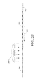
- FIG. 1 depicts a conventional imaging apparatus, where an imaging receiving member 110 such as a photosensitive member or a photoreceptor can be charged on its surface by means of a charger 112 to which a voltage can be supplied from a power supply 111 .
- the imaging receiving member 110 can then be image-wise exposed to light from an optical system or an image input apparatus 113 to form an electrostatic latent image thereon.
- the electrostatic latent image can be developed by bringing a developer mixture from developer station 114 into contact therewith. Development can be effected by use of a magnetic brush, powder cloud, or other known development process.
- the toner particles After the toner particles have been deposited on surface of the imaging receiving member 110 , they can be transferred to an image receiving substrate 116 such as a copy sheet by a transfer means 125 , which can be pressure transfer or electrostatic transfer. Alternatively, the developed image can be transferred to an intermediate transfer member and subsequently transferred to a copy sheet.
- the image receiving substrate 116 can advance to fusing subsystem 119 including a fusing member 120 and a pressure member 121 , wherein the toner image is fused to the image receiving substrate 116 by passing the image receiving substrate 116 between the fusing member 120 and pressure member 121 , thereby forming a permanent image.
- the imaging receiving member 110 subsequent to transfer, can advance to a cleaning station 117 , wherein any toner left on the imaging receiving member 110 is cleaned there-from by use of a blade 122 , brush, or other cleaning apparatus.
- fuser consumes over 50% of the total machine energy while less than 10% of the fuser energy is used for the fusing process. This is because the heat needed to melt toner is transferred from fuser/pressure members, while toner materials cannot be actively heated. For fusing systems, energy is wasted in warming up paper and heating the fuser/pressure members during operation and standby. Additionally, when release agent is applied for effective release of toner images from the fuser member, chemical reactions often occur between the toner materials and release agents under high temperature and pressure that are conventionally used. This leads to low energy efficiency, print defects, and limited life time of fuser members.
- an apparatus for forming an image can include an image receiving member comprising a toner image deposited thereon, wherein the toner image comprises one or more opto-thermal elements incorporated with a polymer. It can further include an intermediate transfer member for transferring the toner image from the image receiving member to an image receiving substrate and one or more light sources configured in proximity to the toner image comprising the one or more opto-thermal elements to optically induce the one or more opto-thermal elements to heat the toner image on the image receiving substrate.
- a method of forming an image can include incorporating one or more opto-thermal elements into a toner composition to form an opto-thermal toner and depositing the opto-thermal toner on an image receiving member to form a toner image.
- the method can further include transferring the toner image from the image receiving member to an image receiving substrate and exposing the one or more opto-thermal elements in the toner image to an optical signal to generate heat to fix the toner image on the image receiving substrate.
- another method of forming an image can include depositing a toner image on an image receiving member; the toner image comprising one or more opto-thermal elements and transferring the toner image from the image receiving member to an image receiving substrate.
- the method can further include exposing the one or more opto-thermal elements in the toner image to an optical signal to heat the toner image on the image receiving substrate and passing the image receiving substrate through a contact arc formed by a fuser member and a pressure member to fix the toner image on the image receiving substrate.
- FIG. 1 depicts a conventional imaging apparatus.
- FIGS. 2A-2B depict an exemplary apparatus and method for forming an image in accordance with various embodiments of the present teachings.
- FIGS. 3A-3B depict another exemplary apparatus and method for forming an image in accordance with various embodiments of the present teachings.
- Exemplary imaging apparatus can include one or more light sources configured to treat toner images after they are transferred on an image receiving substrate (e.g., a copy sheet).
- the toner images can be formed of an opto-thermal toner containing opto-thermal elements in a toner composition.
- the term “opto-thermal elements” refers to elements capable of exhibiting a thermal behavior in response to an optical signal or exhibiting an optical behavior in response to a thermal signal.
- the opto-thermal elements can generate heat in response to exposure or illumination of light.
- the opto-thermal elements can include light induced heating elements.
- the light induced heating elements can include those described in U.S. patent application Ser. No. 12/257,015, entitled “Nanomaterial Heating Element for Fusing Applications,” which is commonly assigned to Xerox Corp., and incorporated by reference in its entirety herein.
- the term “opto-thermal toner” refers to a toner or toner composition including opto-thermal elements.
- toner can be referred to as “toner composition” and vice versa.
- the toner can be any known toner including, for example, emulsion/aggregation (EA) toner, liquid toner, or other suitable toner composition.
- EA emulsion/aggregation
- the toner can include polymer(s), e.g., known as toner resins.
- the opto-thermal elements can be incorporated with polymers in the toner composition such that the opto-thermal elements can be exposed to or otherwise receive an optical signal (e.g., from a light illumination).
- the polymers can be optically transparent to the optical signal.
- the opto-thermal elements can be at least partially exposed to the surface of the toner.
- the disclosed polymers and toner composition can include those disclosed in U.S. patent application Ser. No. 12/272,412, entitled “Toners Including Carbon Nanotubes Dispersed in a Polymer Matrix”, which is commonly assigned to Xerox Corp. and incorporated by reference in its entirety herein.
- optically transparent polymers refers to polymers optically transparent to an extent that does not affect opto-thermal effect of the opto-thermal elements that are incorporated therewith.
- the optically transparent polymers can have from about 10% to about 100% transparency, or from about 10% to about 60% transparency, or from about 30% to about 90% transparency in the absorption range of the opto-thermal elements.
- Exemplary optically transparent polymers can include, but are not limited to, polycarbonate, PET, PMMA, nanocomposite polymers and conducting polymers like polythiophene and polyaniline and its derivatives.
- the opto-thermal elements can be physically dispersed in and/or chemically bonded to the toner resins.
- the opto-thermal elements being “bonded” to the toner resins refers to chemical bonding such as ionic or covalent bonding, and not to weaker bonding mechanisms such as hydrogen bonding or physical entrapment of molecules that may occur when two chemical species are in close proximity to each other.
- the physical dispersing can include processes of, e.g., extrusion, melt spinning or melt blowing, while the chemical bonding can include, e.g., in situ polymerization by functionalization of opto-thermal elements.
- the opto-thermal elements can be incorporated with polymers in a toner in an amount to allow for related toner images at least partially heated, fused, and/or fixed on an image receiving substrate, wherein a fuser subsystem may or may not be used in the imaging apparatus. Additionally, the amount of opto-thermal elements can be sufficiently low without affecting toner colors. In embodiments, the opto-thermal elements can be present in an amount ranging from about 0.1% to about 60%, or from about 0.1% to about 10%, or from about 10% to about 60% by weight, relative to a total of polymer(s) in the toner.
- the opto-thermal elements can have a density ranging from about 0.01 g/cm 3 to about 10 g/cm 3 ; or from about 0.01 g/cm 3 to about 1 g/cm 3 , or from about 1 g/cm 3 to about 10 g/cm 3 .
- the opto-thermal elements can achieve at least a local temperature in a range of about 50° C. to about 1500° C., or from about 50° to about 500° C., or from about 0.500° to about 1500° C. and can go to a desired lower temperature rapidly upon removal of the light exposure.
- This temperature can locally heat/fuse the toner but not the underlying image receiving substrate (e.g., a copy sheet).
- the time taken to reach desired temperature and to return to ambient temperature can depend on several factors, such as, for example, light source, opto-thermal element, spectral power distribution of the light source, intensity of the light source, loading, density, of the opto-thermal element, and process speed.
- the opto-thermal elements can be in any shape and/or dimensions.
- the opto-thermal elements can have various cross sectional shapes, such as, for example, rectangular, polygonal, oval, or circular shapes.
- the opto-thermal elements can be nanoparticles having an average particle size ranging from about ⁇ (less than) 1 nm to about 500 nm, or from about ⁇ 1 nm to about 50 nm, or from about 50 nm to about 500 nm.
- the nanoparticles can have an average aspect ratio ranging from about 1 to about 10 8 :1, or from about 10:1 to about 10 7 :1, or from about 100:1 to about 10 6 :1.
- the opto-thermal elements can include nano-materials, such as, for example, carbon nanotubes (CNTs), graphene, metal nanoshells, metal nanostructures, and/or their combinations.
- CNTs carbon nanotubes
- graphene graphene
- metal nanoshells metal nanostructures
- metal nanostructures and/or their combinations.
- carbon nanotubes can be considered as one atom thick layers of graphite, called graphene sheets, rolled up into nanometer-sized cylinders, tubes or other shapes.
- Exemplary carbon nanotubes can include single wall carbon nanotubes (SWNTs), double wall carbon nanotubes (DWNTs), and multiple wall carbon nanotubes (MWNTs), and/or their various functionalized and derivatized fibril forms such as nanofibers.
- SWNTs single wall carbon nanotubes
- DWNTs double wall carbon nanotubes
- MWNTs multiple wall carbon nanotubes
- the term “carbon nanotubes” can include modified CNTs from all possible nanotubes described there above and their combinations.
- the modification of the nanotubes can include a physical and/or a chemical modification.
- the carbon nanotubes may be functionalized with one or more chemical moieties.
- the chemical moiety on the carbon nanotubes can generally covalently attach to a suitable monomer.
- the monomers then polymerize by any suitable means known in the art, thereby forming carbon nanotubes dispersed in a polymer matrix.
- This carbon nanotube/polymer composite resin can be incorporated into a toner.
- the carbon nanotubes can be of different lengths, diameters, and/or chiralities.
- the CNTs can have an average diameter ranging from about 0.1 nm to about 100 nm, from about 0.5 to about 50 nm, or from about 1 nm to about 100 nm.
- the CNTs can have a length ranging from about 10 nm to about 5 mm, about 200 nm to about 10 microns, or about 500 nm to about 1 micron.
- the CNTs can have an average surface area ranging from about 50 m 2 /g to about 3000 m 2 /g, from about 50 m 2 /g to about 1500 m 2 /g, or from about 500 m 2 /g to about 1000 m 2 /g.
- the carbon nanotubes can be obtained in low and/or high purity dried paper forms or can be purchased in various solutions. In other embodiments, the carbon nanotubes can be available in the as-processed unpurified condition, where a purification process can be subsequently carried out.
- the opto-thermal elements can include metal nanoshells.
- Exemplary metal nanoshells can include those disclosed in U.S. patent Ser. No. 12/257,015.
- the metal nanoshell can include a dielectric core and a metal shell disposed over the dielectric core.
- the metal in the metal shell can be selected from the group consisting of gold, silver, and copper.
- the dielectric core can be selected from the group consisting of silica, titania, and alumina.
- the dielectric core in the metal nanoshell can have a diameter from about 30 nm to about 150 nm and in some cases from about 50 nm to 70 nm with metal shell having a thickness from about 5 nm to about 25 nm and in some cases from about 10 nm to about 15 nm.
- the opto-thermal toner in addition to opto-thermal elements incorporated polymer, can optionally include one or more colorants and optionally one or more waxes.
- Exemplary colorants and waxes can include those disclosed in U.S. patent Ser. No. 12/272,412.
- the colorants can be carbon black and the waxes can be polyolefin waxes.
- light sources can be used to provide the optical signal.
- light sources can have an emission in the absorption range of the opto-thermal elements such that heat can be produced by light absorption of the opto-thermal elements from the light sources.
- Toner images containing opto-thermal elements can then be heated, fused, and/or fixed on the underlying surface.
- the light source(s) can include at least one of a UV lamp, a xenon lamp, a halogen lamp, a laser array, a light emitting diode (LED) array, and an organic light emitting diode (OLED) array.
- the light source can emit light anywhere from ultraviolet to near infrared region.
- the light source can be a digital light source, wherein each light component of the at least one of the laser array, the light emitting diode (LED) array, and the organic light emitting diode (OLED) array can be individually addressable.
- the term “light component” as used herein refers to an LED of the LED array, an OLED of the OLED array or a laser of the Laser array.
- each light component such as an LED of the LED array can be identified and manipulated independently of its surrounding LEDs, for example, each LED or each group of LEDs can be individually turned on or off and output of each LED or each group of LEDs can be controlled individually.
- the light components such as for example one or more LEDs of the LED array corresponding to the text can be turned on to selectively expose light on those portions of the one or more opto-thermal elements that correspond to the text, but the LEDs corresponding to the line spacing between the text and the margins around the text can be turned off.
- the opto-thermal elements can be a digital heat source.
- the light source(s) can be selected according to the opto-thermal toner used for forming toner images, or vice versa.
- the imaging apparatus can have various configurations.
- the exemplary imaging apparatus 200 A does not include a fuser subsystem as depicted in FIG. 1 .
- one or more light sources 260 can be configured to fuse/fix toner images formed of an opto-thermal toner on the image receiving substrate 116 .
- toner images formed of the opto-thermal toner can be deposited on an image receiving member 110 and then transferred to the image receiving substrate 116 by an intermediate transfer member 125 .
- the light source 260 can emit light to optically induce an opto-thermal effect of the opto-thermal elements contained in the toner images. Heat can then be generated due to this optically induced heating effect.
- the toner images 202 can then be heated, fused, and fixed on the imaging receiving substrate 116 to form fixed toner images 208 without using a fuser subsystem.
- the light source(s) 260 can have a power and/or intensity sufficient to completely heat/fuse/fix the toner images on the image receiving substrate 116 .
- the light source(s) 260 can have a high power ranging from about 100 mW/cm 2 to about 50 W/cm 2 , from about 500 mW/cm 2 to about 5 W/cm 2 , or from about 5 W/cm 2 to about 50 W/cm 2 . In this manner, by using light sources 260 , a non-contact fusing/fixing of toner images 202 (see FIGS. 2A-2B ) can be performed.
- the light source(s) 360 can be incorporated into a fuser subsystem for fusing/fixing toner images 202 formed of an opto-thermal toner. As shown, the light source(s) 360 can be used to pre-treat toner image 202 on the image receiving substrate 116 prior to passing the image receiving substrate 116 through a fuser subsystem 319 . The pre-treatment can pre-heat or at least partially melt the toner image 202 to facilitate the subsequent fusing by the fuser subsystem 319 .
- the fuser subsystem 319 can include a fuser member 320 and a backup or pressure member 321 configured as known to one of ordinary skill in the art.
- Each of the fuser member 320 and the pressure member 321 can be a roll member (see FIG. 3A ), a belt member, and any possible combinations thereof as known in the art.
- the fuser member 320 and the pressure member 321 can cooperate to form a nip or contact arc through which the image receiving substrate 116 , having pre-heated toner images 304 thereon, passes. Toner images 308 can then be fixed on the image receiving substrate 116 .
- the temperature and pressure required for fusing/fixing the toner images using the fuser subsystem can be significantly reduced as compared with conventional fuser subsystem.
- conventional fusing process without using the light source(s) 360 , can be performed at a temperature ranging from about 60° C. (140° F.) to about 300° C. (572° F.).
- the disclosed fusing process by the fuser subsystem 319 can be performed at a temperature ranging from about 110° F. to about 450° F., from about 120° F. to about 400° F., or from about 130° F. to about 300° F.
- a pressure can be applied during the fusing process by the backup or pressure member 321 .
- conventional fusing process can be performed at a pressure ranging from about 50 to about 150 Psi.
- the fusing process by the fuser subsystem 319 can be performed at a pressure ranging from about 20 Psi to about 130 Psi, from about 30 Psi to about 120 Psi, or from about 40 to about 110 Psi.
- the fused toner images 308 can be completely formed on the image receiving substrate 116 .
- the light source(s) 360 can have a power and/or intensity that may be lower than the light source(s) 260 depicted in FIGS. 2A-2B for pre-heating toner images.
- the light source(s) 360 can have a low power ranging from about 0.01 W/cm 2 to about 10 W/cm 2 , from about 0.05 W/cm 2 to about 5 W/cm 2 , or from about 0.1 W/cm 2 to about 1 W/cm 2 .
Abstract
Description
Claims (20)
Priority Applications (3)
| Application Number | Priority Date | Filing Date | Title |
|---|---|---|---|
| US13/352,105 US8718528B2 (en) | 2012-01-17 | 2012-01-17 | Efficient fusing and fixing for toners comprising opto-thermal elements |
| JP2013000717A JP5965323B2 (en) | 2012-01-17 | 2013-01-07 | Efficient melting and fixing for toners containing photothermal elements |
| DE102013200190.8A DE102013200190B4 (en) | 2012-01-17 | 2013-01-09 | IMAGE FORMING DEVICE AND IMAGE FORMING METHOD |
Applications Claiming Priority (1)
| Application Number | Priority Date | Filing Date | Title |
|---|---|---|---|
| US13/352,105 US8718528B2 (en) | 2012-01-17 | 2012-01-17 | Efficient fusing and fixing for toners comprising opto-thermal elements |
Publications (2)
| Publication Number | Publication Date |
|---|---|
| US20130183073A1 US20130183073A1 (en) | 2013-07-18 |
| US8718528B2 true US8718528B2 (en) | 2014-05-06 |
Family
ID=48693344
Family Applications (1)
| Application Number | Title | Priority Date | Filing Date |
|---|---|---|---|
| US13/352,105 Active 2032-05-25 US8718528B2 (en) | 2012-01-17 | 2012-01-17 | Efficient fusing and fixing for toners comprising opto-thermal elements |
Country Status (3)
| Country | Link |
|---|---|
| US (1) | US8718528B2 (en) |
| JP (1) | JP5965323B2 (en) |
| DE (1) | DE102013200190B4 (en) |
Cited By (2)
| Publication number | Priority date | Publication date | Assignee | Title |
|---|---|---|---|---|
| US10248038B1 (en) | 2018-01-23 | 2019-04-02 | Xerox Corporation | Graphene-containing toners and related methods |
| US10353325B2 (en) | 2015-01-21 | 2019-07-16 | Hp Indigo B.V. | Liquid electrophotographic composition |
Families Citing this family (3)
| Publication number | Priority date | Publication date | Assignee | Title |
|---|---|---|---|---|
| JP2015179190A (en) * | 2014-03-19 | 2015-10-08 | 富士ゼロックス株式会社 | Image forming apparatus, fixing device, drying device, developer, and droplet for image formation |
| US9243141B1 (en) * | 2014-11-03 | 2016-01-26 | Xerox Corporation | Coated silver nanoparticle composites comprising a sulfonated polyester matrix and methods of making the same |
| JP7035475B2 (en) * | 2017-11-20 | 2022-03-15 | コニカミノルタ株式会社 | Image forming method and image forming device |
Citations (12)
| Publication number | Priority date | Publication date | Assignee | Title |
|---|---|---|---|---|
| US4897691A (en) * | 1986-05-01 | 1990-01-30 | Xerox Corporation | Apparatus for drying and fusing a liquid image to a copy sheet |
| US20080101804A1 (en) * | 2006-10-26 | 2008-05-01 | Kyocera Mita Corporation | Image forming apparatus |
| US20080101832A1 (en) * | 2006-10-25 | 2008-05-01 | Fuji Xerox Co., Ltd. | Image forming apparatus and fixing device |
| US7452645B2 (en) * | 2004-07-16 | 2008-11-18 | Ricoh Company, Ltd. | Toner for developing electrostatic image, method for producing the same, developer, image forming apparatus, process cartridge, and image forming method |
| US7495599B2 (en) | 2005-05-23 | 2009-02-24 | Vaisala Oyj | Simultaneous dual polarization radar system with pedestal mounted receiver |
| US20090297234A1 (en) * | 2008-05-27 | 2009-12-03 | Cahill David F | Pressure roller interframe oil cleaning device and method |
| US7682542B2 (en) * | 2006-06-22 | 2010-03-23 | Eastman Kodak Company | Method of making fuser member |
| US20100104332A1 (en) * | 2008-10-23 | 2010-04-29 | Xerox Corporation | Nanomaterial heating element for fusing applications |
| US20100124713A1 (en) * | 2008-11-17 | 2010-05-20 | Xerox Corporation | Toners including carbon nanotubes dispersed in a polymer matrix |
| US7745080B2 (en) * | 2004-03-19 | 2010-06-29 | Fuji Xerox Co., Ltd. | Color image forming developer, color image forming method, and color image forming device |
| US7754408B2 (en) | 2005-09-29 | 2010-07-13 | Xerox Corporation | Synthetic carriers |
| US7851111B2 (en) | 2006-07-31 | 2010-12-14 | Xerox Corporation | Imaging belt with nanotube backing layer, and image forming devices including the same |
Family Cites Families (4)
| Publication number | Priority date | Publication date | Assignee | Title |
|---|---|---|---|---|
| JP2007219103A (en) * | 2006-02-15 | 2007-08-30 | Fuji Xerox Co Ltd | Electrophotographic toner, electrophotographic developer and image forming method |
| WO2008130201A2 (en) | 2007-04-24 | 2008-10-30 | Nano Interface Technology | Laminate sheet for electromagnetic radiation shielding and grounding |
| JP2011008162A (en) * | 2009-06-29 | 2011-01-13 | Fuji Xerox Co Ltd | Toner for electrostatic charge image development, method for producing toner for electrostatic charge image development, electrostatic charge image developer, toner cartridge, process cartridge, image forming method, and image forming apparatus |
| JP2012103535A (en) * | 2010-11-11 | 2012-05-31 | Fuji Xerox Co Ltd | Toner for electrostatic charge image development, electrostatic charge image developer, toner cartridge, process cartridge, image forming method, and image forming apparatus |
-
2012
- 2012-01-17 US US13/352,105 patent/US8718528B2/en active Active
-
2013
- 2013-01-07 JP JP2013000717A patent/JP5965323B2/en active Active
- 2013-01-09 DE DE102013200190.8A patent/DE102013200190B4/en active Active
Patent Citations (12)
| Publication number | Priority date | Publication date | Assignee | Title |
|---|---|---|---|---|
| US4897691A (en) * | 1986-05-01 | 1990-01-30 | Xerox Corporation | Apparatus for drying and fusing a liquid image to a copy sheet |
| US7745080B2 (en) * | 2004-03-19 | 2010-06-29 | Fuji Xerox Co., Ltd. | Color image forming developer, color image forming method, and color image forming device |
| US7452645B2 (en) * | 2004-07-16 | 2008-11-18 | Ricoh Company, Ltd. | Toner for developing electrostatic image, method for producing the same, developer, image forming apparatus, process cartridge, and image forming method |
| US7495599B2 (en) | 2005-05-23 | 2009-02-24 | Vaisala Oyj | Simultaneous dual polarization radar system with pedestal mounted receiver |
| US7754408B2 (en) | 2005-09-29 | 2010-07-13 | Xerox Corporation | Synthetic carriers |
| US7682542B2 (en) * | 2006-06-22 | 2010-03-23 | Eastman Kodak Company | Method of making fuser member |
| US7851111B2 (en) | 2006-07-31 | 2010-12-14 | Xerox Corporation | Imaging belt with nanotube backing layer, and image forming devices including the same |
| US20080101832A1 (en) * | 2006-10-25 | 2008-05-01 | Fuji Xerox Co., Ltd. | Image forming apparatus and fixing device |
| US20080101804A1 (en) * | 2006-10-26 | 2008-05-01 | Kyocera Mita Corporation | Image forming apparatus |
| US20090297234A1 (en) * | 2008-05-27 | 2009-12-03 | Cahill David F | Pressure roller interframe oil cleaning device and method |
| US20100104332A1 (en) * | 2008-10-23 | 2010-04-29 | Xerox Corporation | Nanomaterial heating element for fusing applications |
| US20100124713A1 (en) * | 2008-11-17 | 2010-05-20 | Xerox Corporation | Toners including carbon nanotubes dispersed in a polymer matrix |
Cited By (2)
| Publication number | Priority date | Publication date | Assignee | Title |
|---|---|---|---|---|
| US10353325B2 (en) | 2015-01-21 | 2019-07-16 | Hp Indigo B.V. | Liquid electrophotographic composition |
| US10248038B1 (en) | 2018-01-23 | 2019-04-02 | Xerox Corporation | Graphene-containing toners and related methods |
Also Published As
| Publication number | Publication date |
|---|---|
| JP2013148895A (en) | 2013-08-01 |
| US20130183073A1 (en) | 2013-07-18 |
| DE102013200190A1 (en) | 2013-07-18 |
| DE102013200190B4 (en) | 2023-03-16 |
| JP5965323B2 (en) | 2016-08-03 |
Similar Documents
| Publication | Publication Date | Title |
|---|---|---|
| US8718528B2 (en) | Efficient fusing and fixing for toners comprising opto-thermal elements | |
| US8086154B2 (en) | Nanomaterial heating element for fusing applications | |
| JP4937115B2 (en) | Radiation curable toner composition | |
| US7579130B2 (en) | Image transfer sheet for electrophotography, method for manufacturing image recorded medium using the same, and image recorded medium | |
| US6535711B2 (en) | Process for the double-sided printing and/or coating of a substrate | |
| JP2004094146A (en) | Fixing device | |
| JPH04232983A (en) | Composite fixing member | |
| JP4100189B2 (en) | Information recording medium and manufacturing method thereof | |
| JP2010243596A (en) | Image recording medium, image recording medium reusing apparatus, image forming apparatus with the same, and image recording medium reusing method | |
| JP5372265B2 (en) | Image forming system and method | |
| JP2012189698A (en) | Fixing device and image forming apparatus having the same | |
| EP2696247B1 (en) | Fusing unit and image forming apparatus including the same | |
| EP2188675A1 (en) | Peeling member, member for forming peeling member, method of manufacturing peeling member, image remover, image forming and removing system, and image removing method | |
| JP5383172B2 (en) | Photoreceptor for electrophotography | |
| JP2017062323A (en) | Image forming apparatus and image forming method | |
| JP2014502365A (en) | Preheating the steam treatment of the printer | |
| JP2009172499A (en) | Method of manufacturing transfer belt and device for curing surface layer of transfer belt for use in manufacturing the same | |
| JP4168847B2 (en) | Film for laminating with core substrate for information recording medium, method for producing the same, image forming method using the same, and information recording medium | |
| JP6040571B2 (en) | Image forming apparatus | |
| JPH09106206A (en) | Xerographic printer | |
| JP2008180965A (en) | Fixing device, method for manufacturing heating belt, and image forming apparatus | |
| JP2010133988A (en) | Image forming apparatus | |
| JP2019061154A (en) | Tubular body for infrared light fixing device, infrared light fixing device, and image forming apparatus | |
| JP2007156363A (en) | Roller for fixing, fixing device and image forming apparatus | |
| JP2017173541A (en) | Image forming apparatus |
Legal Events
| Date | Code | Title | Description |
|---|---|---|---|
| AS | Assignment |
Owner name: XEROX CORPORATION, CONNECTICUT Free format text: ASSIGNMENT OF ASSIGNORS INTEREST;ASSIGNORS:ZHANG, YUANJIA;KANUNGO, MANDAKINI;KUMAR, SAMIR;AND OTHERS;SIGNING DATES FROM 20111227 TO 20111228;REEL/FRAME:027546/0597 |
|
| FEPP | Fee payment procedure |
Free format text: PAYOR NUMBER ASSIGNED (ORIGINAL EVENT CODE: ASPN); ENTITY STATUS OF PATENT OWNER: LARGE ENTITY |
|
| STCF | Information on status: patent grant |
Free format text: PATENTED CASE |
|
| MAFP | Maintenance fee payment |
Free format text: PAYMENT OF MAINTENANCE FEE, 4TH YEAR, LARGE ENTITY (ORIGINAL EVENT CODE: M1551) Year of fee payment: 4 |
|
| MAFP | Maintenance fee payment |
Free format text: PAYMENT OF MAINTENANCE FEE, 8TH YEAR, LARGE ENTITY (ORIGINAL EVENT CODE: M1552); ENTITY STATUS OF PATENT OWNER: LARGE ENTITY Year of fee payment: 8 |
|
| AS | Assignment |
Owner name: CITIBANK, N.A., AS AGENT, DELAWARE Free format text: SECURITY INTEREST;ASSIGNOR:XEROX CORPORATION;REEL/FRAME:062740/0214 Effective date: 20221107 |
|
| AS | Assignment |
Owner name: XEROX CORPORATION, CONNECTICUT Free format text: RELEASE OF SECURITY INTEREST IN PATENTS AT R/F 062740/0214;ASSIGNOR:CITIBANK, N.A., AS AGENT;REEL/FRAME:063694/0122 Effective date: 20230517 |
|
| AS | Assignment |
Owner name: CITIBANK, N.A., AS COLLATERAL AGENT, NEW YORK Free format text: SECURITY INTEREST;ASSIGNOR:XEROX CORPORATION;REEL/FRAME:064760/0389 Effective date: 20230621 |
|
| AS | Assignment |
Owner name: JEFFERIES FINANCE LLC, AS COLLATERAL AGENT, NEW YORK Free format text: SECURITY INTEREST;ASSIGNOR:XEROX CORPORATION;REEL/FRAME:065628/0019 Effective date: 20231117 |
|
| AS | Assignment |
Owner name: CITIBANK, N.A., AS COLLATERAL AGENT, NEW YORK Free format text: SECURITY INTEREST;ASSIGNOR:XEROX CORPORATION;REEL/FRAME:066741/0001 Effective date: 20240206 |