US8704299B2 - Semiconductor device and manufacturing method thereof - Google Patents
Semiconductor device and manufacturing method thereof Download PDFInfo
- Publication number
- US8704299B2 US8704299B2 US13/736,381 US201313736381A US8704299B2 US 8704299 B2 US8704299 B2 US 8704299B2 US 201313736381 A US201313736381 A US 201313736381A US 8704299 B2 US8704299 B2 US 8704299B2
- Authority
- US
- United States
- Prior art keywords
- gate electrode
- insulating film
- trench
- semiconductor substrate
- impurity diffusion
- Prior art date
- Legal status (The legal status is an assumption and is not a legal conclusion. Google has not performed a legal analysis and makes no representation as to the accuracy of the status listed.)
- Expired - Fee Related
Links
- 239000004065 semiconductor Substances 0.000 title claims abstract description 177
- 238000004519 manufacturing process Methods 0.000 title description 21
- 238000009792 diffusion process Methods 0.000 claims abstract description 118
- 239000012535 impurity Substances 0.000 claims abstract description 102
- 238000002955 isolation Methods 0.000 claims description 111
- 239000000758 substrate Substances 0.000 claims description 103
- 230000015572 biosynthetic process Effects 0.000 claims description 21
- 239000011229 interlayer Substances 0.000 claims description 17
- 239000003990 capacitor Substances 0.000 claims description 11
- 239000002344 surface layer Substances 0.000 claims description 4
- VYPSYNLAJGMNEJ-UHFFFAOYSA-N Silicium dioxide Chemical compound O=[Si]=O VYPSYNLAJGMNEJ-UHFFFAOYSA-N 0.000 description 50
- 108091006146 Channels Proteins 0.000 description 26
- 239000010410 layer Substances 0.000 description 24
- 229910052814 silicon oxide Inorganic materials 0.000 description 20
- 229910052581 Si3N4 Inorganic materials 0.000 description 17
- HQVNEWCFYHHQES-UHFFFAOYSA-N silicon nitride Chemical compound N12[Si]34N5[Si]62N3[Si]51N64 HQVNEWCFYHHQES-UHFFFAOYSA-N 0.000 description 17
- 229910052681 coesite Inorganic materials 0.000 description 16
- 229910052906 cristobalite Inorganic materials 0.000 description 16
- 239000000377 silicon dioxide Substances 0.000 description 16
- 229910052682 stishovite Inorganic materials 0.000 description 16
- 229910052905 tridymite Inorganic materials 0.000 description 16
- NRTOMJZYCJJWKI-UHFFFAOYSA-N Titanium nitride Chemical compound [Ti]#N NRTOMJZYCJJWKI-UHFFFAOYSA-N 0.000 description 12
- 238000010586 diagram Methods 0.000 description 11
- WFKWXMTUELFFGS-UHFFFAOYSA-N tungsten Chemical compound [W] WFKWXMTUELFFGS-UHFFFAOYSA-N 0.000 description 11
- 239000010937 tungsten Substances 0.000 description 11
- 229910052721 tungsten Inorganic materials 0.000 description 11
- 238000005530 etching Methods 0.000 description 9
- 238000000034 method Methods 0.000 description 7
- 230000006870 function Effects 0.000 description 6
- 230000015556 catabolic process Effects 0.000 description 5
- 238000006731 degradation reaction Methods 0.000 description 5
- 230000003647 oxidation Effects 0.000 description 5
- 238000007254 oxidation reaction Methods 0.000 description 5
- XUIMIQQOPSSXEZ-UHFFFAOYSA-N Silicon Chemical compound [Si] XUIMIQQOPSSXEZ-UHFFFAOYSA-N 0.000 description 4
- 238000001312 dry etching Methods 0.000 description 4
- 150000002500 ions Chemical class 0.000 description 4
- 230000014759 maintenance of location Effects 0.000 description 4
- 230000005012 migration Effects 0.000 description 4
- 238000013508 migration Methods 0.000 description 4
- 229910021420 polycrystalline silicon Inorganic materials 0.000 description 4
- 229920005591 polysilicon Polymers 0.000 description 4
- 229910052710 silicon Inorganic materials 0.000 description 4
- 239000010703 silicon Substances 0.000 description 4
- 238000009825 accumulation Methods 0.000 description 3
- 238000005229 chemical vapour deposition Methods 0.000 description 3
- 238000009826 distribution Methods 0.000 description 3
- 230000000694 effects Effects 0.000 description 3
- 238000005468 ion implantation Methods 0.000 description 3
- 239000011295 pitch Substances 0.000 description 3
- 239000002356 single layer Substances 0.000 description 3
- 108010075750 P-Type Calcium Channels Proteins 0.000 description 2
- OAICVXFJPJFONN-UHFFFAOYSA-N Phosphorus Chemical compound [P] OAICVXFJPJFONN-UHFFFAOYSA-N 0.000 description 2
- QVGXLLKOCUKJST-UHFFFAOYSA-N atomic oxygen Chemical compound [O] QVGXLLKOCUKJST-UHFFFAOYSA-N 0.000 description 2
- 230000008901 benefit Effects 0.000 description 2
- 230000008859 change Effects 0.000 description 2
- 239000011521 glass Substances 0.000 description 2
- 230000001771 impaired effect Effects 0.000 description 2
- 229910052760 oxygen Inorganic materials 0.000 description 2
- 239000001301 oxygen Substances 0.000 description 2
- 230000002093 peripheral effect Effects 0.000 description 2
- 229910052698 phosphorus Inorganic materials 0.000 description 2
- 239000011574 phosphorus Substances 0.000 description 2
- 238000005498 polishing Methods 0.000 description 2
- 235000012239 silicon dioxide Nutrition 0.000 description 2
- LIVNPJMFVYWSIS-UHFFFAOYSA-N silicon monoxide Chemical class [Si-]#[O+] LIVNPJMFVYWSIS-UHFFFAOYSA-N 0.000 description 2
- 230000002411 adverse Effects 0.000 description 1
- 238000007796 conventional method Methods 0.000 description 1
- 238000013500 data storage Methods 0.000 description 1
- 230000006735 deficit Effects 0.000 description 1
- 238000001035 drying Methods 0.000 description 1
- 239000007789 gas Substances 0.000 description 1
- 239000000463 material Substances 0.000 description 1
- 239000000203 mixture Substances 0.000 description 1
- 229910021421 monocrystalline silicon Inorganic materials 0.000 description 1
- 230000009467 reduction Effects 0.000 description 1
- 230000001105 regulatory effect Effects 0.000 description 1
- 238000003860 storage Methods 0.000 description 1
- 239000000126 substance Substances 0.000 description 1
- 238000001039 wet etching Methods 0.000 description 1
Images


Classifications
-
- H—ELECTRICITY
- H01—ELECTRIC ELEMENTS
- H01L—SEMICONDUCTOR DEVICES NOT COVERED BY CLASS H10
- H01L29/00—Semiconductor devices adapted for rectifying, amplifying, oscillating or switching, or capacitors or resistors with at least one potential-jump barrier or surface barrier, e.g. PN junction depletion layer or carrier concentration layer; Details of semiconductor bodies or of electrodes thereof ; Multistep manufacturing processes therefor
- H01L29/40—Electrodes ; Multistep manufacturing processes therefor
- H01L29/41—Electrodes ; Multistep manufacturing processes therefor characterised by their shape, relative sizes or dispositions
- H01L29/423—Electrodes ; Multistep manufacturing processes therefor characterised by their shape, relative sizes or dispositions not carrying the current to be rectified, amplified or switched
- H01L29/42312—Gate electrodes for field effect devices
- H01L29/42316—Gate electrodes for field effect devices for field-effect transistors
- H01L29/4232—Gate electrodes for field effect devices for field-effect transistors with insulated gate
- H01L29/42356—Disposition, e.g. buried gate electrode
- H01L29/4236—Disposition, e.g. buried gate electrode within a trench, e.g. trench gate electrode, groove gate electrode
-
- H—ELECTRICITY
- H01—ELECTRIC ELEMENTS
- H01L—SEMICONDUCTOR DEVICES NOT COVERED BY CLASS H10
- H01L29/00—Semiconductor devices adapted for rectifying, amplifying, oscillating or switching, or capacitors or resistors with at least one potential-jump barrier or surface barrier, e.g. PN junction depletion layer or carrier concentration layer; Details of semiconductor bodies or of electrodes thereof ; Multistep manufacturing processes therefor
- H01L29/02—Semiconductor bodies ; Multistep manufacturing processes therefor
- H01L29/06—Semiconductor bodies ; Multistep manufacturing processes therefor characterised by their shape; characterised by the shapes, relative sizes, or dispositions of the semiconductor regions ; characterised by the concentration or distribution of impurities within semiconductor regions
- H01L29/10—Semiconductor bodies ; Multistep manufacturing processes therefor characterised by their shape; characterised by the shapes, relative sizes, or dispositions of the semiconductor regions ; characterised by the concentration or distribution of impurities within semiconductor regions with semiconductor regions connected to an electrode not carrying current to be rectified, amplified or switched and such electrode being part of a semiconductor device which comprises three or more electrodes
- H01L29/1025—Channel region of field-effect devices
- H01L29/1029—Channel region of field-effect devices of field-effect transistors
- H01L29/1033—Channel region of field-effect devices of field-effect transistors with insulated gate, e.g. characterised by the length, the width, the geometric contour or the doping structure
- H01L29/1037—Channel region of field-effect devices of field-effect transistors with insulated gate, e.g. characterised by the length, the width, the geometric contour or the doping structure and non-planar channel
-
- H—ELECTRICITY
- H01—ELECTRIC ELEMENTS
- H01L—SEMICONDUCTOR DEVICES NOT COVERED BY CLASS H10
- H01L29/00—Semiconductor devices adapted for rectifying, amplifying, oscillating or switching, or capacitors or resistors with at least one potential-jump barrier or surface barrier, e.g. PN junction depletion layer or carrier concentration layer; Details of semiconductor bodies or of electrodes thereof ; Multistep manufacturing processes therefor
- H01L29/40—Electrodes ; Multistep manufacturing processes therefor
- H01L29/41—Electrodes ; Multistep manufacturing processes therefor characterised by their shape, relative sizes or dispositions
- H01L29/423—Electrodes ; Multistep manufacturing processes therefor characterised by their shape, relative sizes or dispositions not carrying the current to be rectified, amplified or switched
- H01L29/42312—Gate electrodes for field effect devices
- H01L29/42316—Gate electrodes for field effect devices for field-effect transistors
- H01L29/4232—Gate electrodes for field effect devices for field-effect transistors with insulated gate
- H01L29/42364—Gate electrodes for field effect devices for field-effect transistors with insulated gate characterised by the insulating layer, e.g. thickness or uniformity
- H01L29/42368—Gate electrodes for field effect devices for field-effect transistors with insulated gate characterised by the insulating layer, e.g. thickness or uniformity the thickness being non-uniform
-
- H—ELECTRICITY
- H01—ELECTRIC ELEMENTS
- H01L—SEMICONDUCTOR DEVICES NOT COVERED BY CLASS H10
- H01L29/00—Semiconductor devices adapted for rectifying, amplifying, oscillating or switching, or capacitors or resistors with at least one potential-jump barrier or surface barrier, e.g. PN junction depletion layer or carrier concentration layer; Details of semiconductor bodies or of electrodes thereof ; Multistep manufacturing processes therefor
- H01L29/66—Types of semiconductor device ; Multistep manufacturing processes therefor
- H01L29/66007—Multistep manufacturing processes
- H01L29/66075—Multistep manufacturing processes of devices having semiconductor bodies comprising group 14 or group 13/15 materials
- H01L29/66227—Multistep manufacturing processes of devices having semiconductor bodies comprising group 14 or group 13/15 materials the devices being controllable only by the electric current supplied or the electric potential applied, to an electrode which does not carry the current to be rectified, amplified or switched, e.g. three-terminal devices
- H01L29/66409—Unipolar field-effect transistors
- H01L29/66477—Unipolar field-effect transistors with an insulated gate, i.e. MISFET
- H01L29/66568—Lateral single gate silicon transistors
- H01L29/66613—Lateral single gate silicon transistors with a gate recessing step, e.g. using local oxidation
- H01L29/66621—Lateral single gate silicon transistors with a gate recessing step, e.g. using local oxidation using etching to form a recess at the gate location
-
- H—ELECTRICITY
- H01—ELECTRIC ELEMENTS
- H01L—SEMICONDUCTOR DEVICES NOT COVERED BY CLASS H10
- H01L29/00—Semiconductor devices adapted for rectifying, amplifying, oscillating or switching, or capacitors or resistors with at least one potential-jump barrier or surface barrier, e.g. PN junction depletion layer or carrier concentration layer; Details of semiconductor bodies or of electrodes thereof ; Multistep manufacturing processes therefor
- H01L29/66—Types of semiconductor device ; Multistep manufacturing processes therefor
- H01L29/68—Types of semiconductor device ; Multistep manufacturing processes therefor controllable by only the electric current supplied, or only the electric potential applied, to an electrode which does not carry the current to be rectified, amplified or switched
- H01L29/76—Unipolar devices, e.g. field effect transistors
- H01L29/772—Field effect transistors
- H01L29/78—Field effect transistors with field effect produced by an insulated gate
- H01L29/7827—Vertical transistors
-
- H—ELECTRICITY
- H10—SEMICONDUCTOR DEVICES; ELECTRIC SOLID-STATE DEVICES NOT OTHERWISE PROVIDED FOR
- H10B—ELECTRONIC MEMORY DEVICES
- H10B12/00—Dynamic random access memory [DRAM] devices
- H10B12/01—Manufacture or treatment
- H10B12/02—Manufacture or treatment for one transistor one-capacitor [1T-1C] memory cells
- H10B12/05—Making the transistor
- H10B12/053—Making the transistor the transistor being at least partially in a trench in the substrate
-
- H—ELECTRICITY
- H10—SEMICONDUCTOR DEVICES; ELECTRIC SOLID-STATE DEVICES NOT OTHERWISE PROVIDED FOR
- H10B—ELECTRONIC MEMORY DEVICES
- H10B12/00—Dynamic random access memory [DRAM] devices
- H10B12/30—DRAM devices comprising one-transistor - one-capacitor [1T-1C] memory cells
- H10B12/34—DRAM devices comprising one-transistor - one-capacitor [1T-1C] memory cells the transistor being at least partially in a trench in the substrate
-
- H—ELECTRICITY
- H01—ELECTRIC ELEMENTS
- H01L—SEMICONDUCTOR DEVICES NOT COVERED BY CLASS H10
- H01L29/00—Semiconductor devices adapted for rectifying, amplifying, oscillating or switching, or capacitors or resistors with at least one potential-jump barrier or surface barrier, e.g. PN junction depletion layer or carrier concentration layer; Details of semiconductor bodies or of electrodes thereof ; Multistep manufacturing processes therefor
- H01L29/02—Semiconductor bodies ; Multistep manufacturing processes therefor
- H01L29/06—Semiconductor bodies ; Multistep manufacturing processes therefor characterised by their shape; characterised by the shapes, relative sizes, or dispositions of the semiconductor regions ; characterised by the concentration or distribution of impurities within semiconductor regions
- H01L29/08—Semiconductor bodies ; Multistep manufacturing processes therefor characterised by their shape; characterised by the shapes, relative sizes, or dispositions of the semiconductor regions ; characterised by the concentration or distribution of impurities within semiconductor regions with semiconductor regions connected to an electrode carrying current to be rectified, amplified or switched and such electrode being part of a semiconductor device which comprises three or more electrodes
- H01L29/0843—Source or drain regions of field-effect devices
- H01L29/0847—Source or drain regions of field-effect devices of field-effect transistors with insulated gate
Definitions
- This invention relates to a semiconductor device and a manufacturing method of a semiconductor device.
- DRAM Dynamic Random Access Memory
- DRAM Dynamic Random Access Memory
- Patent Document 1 Japanese Laid-Open Patent Publication No. 2006-339476 (Patent Document 1) and No. 2007-081095 (Patent Document 2) disclose a so-called trench-gate transistor (also called “recess channel transistor”) in which a gate electrode is embedded in a trench formed in a principal surface of a semiconductor substrate.
- trench-gate transistor also called “recess channel transistor”
- trench-gate transistor makes it possible to ensure a physically sufficient effective channel length (gate length), and to realize a DRAM having minute cells with a minimum processing size of 60 nm or less.
- Patent Document 2 discloses a DRAM having two trenches formed in a semiconductor substrate to be adjacent to each other, a gate electrode formed in each of the trenches via a gate insulating film, a first impurity diffusion region formed on a principal surface of the semiconductor substrate between the two gate electrodes and serving as a common impurity diffusion region for the two gate electrodes, and a second impurity diffusion region formed on the principal surface of the semiconductor substrate located on an element isolation region side of each of the two gate electrodes.
- the channel region of the transistor is formed on three surfaces consisting of the opposite side faces and the bottom face of the trench.
- the inventor has found that if the size of a transistor configured as described above is further reduced, sufficient ON current cannot be obtained for the transistor, and hence the DRAM becomes difficult to operate normally. This is attributable to the fact that the channel resistance is increased due to the transistor channel region being formed on the three surfaces forming the trench.
- a gate electrode is formed to project above the surface of a semiconductor substrate.
- the projected gate electrode itself makes it extremely difficult to form bit wiring and a capacitor in later steps. This poses a problem that manufacturing of a DRAM itself becomes difficult.
- An aspect of the invention provides a semiconductor device including: a plurality of first element isolation regions provided in a semiconductor substrate to extend in a first direction and each defining an active region having a plurality of element formation regions; a gate electrode trench provided in a surface layer of the semiconductor substrate to extend in a second direction intersecting with the first element isolation regions and the active regions, and having first and second side faces facing each other and a bottom; a fin formed such that a part of the active region protrudes from the bottom of the gate electrode trench by forming the gate electrode trench such that a first trench section thereof formed in the active region has a smaller depth than a second trench section thereof formed in the first element isolation region, and the depth of the part of the first trench facing the second trench section is substantially the same as that of the second trench section; a gate insulating film covering the surfaces of the gate electrode trench and the fin; a gate electrode formed to stride over the fin via the gate insulating film by being embedded in a lower part of the gate electrode trench; a first impurity diffusion region formed in the
- the semiconductor substrate is provided with a first impurity diffusion region covering the top part of the gate insulating film disposed on the first side face, a second impurity diffusion region at least covering the gate insulating film disposed on the second side face, and a fin formed such that a part of the active region protrudes from the bottom of the gate electrode trench.
- channel regions are formed on the two surfaces of the bottom of the gate electrode trench and the lower part of the first side face, and on the fin, whereby it is made possible to reduce the channel resistance in comparison with a related semiconductor device in which channel regions are formed on the three surfaces of the bottom and the opposing side faces of the gate electrode trench. This makes it possible to ensure sufficient ON current of transistors.
- another transistor is arranged adjacently on the second side face of the gate electrode trench, so that no channel region is formed between the gate electrode trenches.
- the gate electrode is formed to fill the lower part of the gate electrode trench and to stride over the fin via the gate insulating film, and the embedded insulating film is formed to fill the gate electrode trench and cover the top face of the gate electrode, whereby the gate electrode will not protrude above the surface of the semiconductor substrate.
- figure numbers in FIGS. 3 to 13 with suffix “A” each represent a front view.
- the figure numbers in FIGS. 3 to 13 with suffix “B” are cross-sectional views taken along the line A-A in FIG. 1
- those with suffix “C” are cross-sectional views taken along the line B-B in FIG. 1
- those with suffix “D” are cross-sectional views taken along the line C-C in FIG. 1 .
- any redundant drawings relating to the same structure will be omitted.
- FIG. 1 is a schematic plan view showing a memory cell array provided in a semiconductor device according to an embodiment of the invention
- FIG. 2A is a cross-sectional view of the memory cell array taken along the line A-A in FIG. 1
- FIG. 2B is a cross-sectional view of the memory cell array taken along the line B-B in FIG. 1
- FIG. 2C is a perspective view for explaining a cross-sectional configuration of a fin provided in a gate electrode trench of the semiconductor device according to the embodiment of invention
- FIG. 2D is an enlarged cross-sectional view for explaining thickness of a gate insulating film provided in the semiconductor device according to the embodiment of invention;
- FIG. 3A is diagram illustrating a manufacturing step (step 1 ) of a memory cell array provided in the semiconductor device according to the embodiment of the invention and is a plan view showing a region where the memory cell array is formed
- FIG. 3B is a cross-sectional view of the structure shown in FIG. 3A taken along the line A-A in FIG. 3A
- FIG. 3D is a cross-sectional view of the structure shown in FIG. 3A taken along the line C-C in FIG. 3A ;
- FIG. 4D is a diagram illustrating a manufacturing step (step 2 ) of the memory cell array provided in the semiconductor device according to the embodiment of the invention, following the manufacturing step shown in FIG. 3D ;
- FIG. 5D is a diagram illustrating a manufacturing step (step 3 ) of the memory cell array provided in the semiconductor device according to the embodiment of the invention, following the manufacturing step shown in FIG. 4D ;
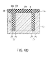
- FIG. 6A is a diagram illustrating a manufacturing step (step 4 ) of the memory cell array provided in the semiconductor device according to the embodiment of the invention, and is a plan view showing a region where the memory cell array is formed
- FIG. 6B is a cross-sectional view of the structure shown in FIG. 6A taken along the line A-A thereof
- FIG. 6D is a cross-sectional view of the structure shown in FIG. 6A taken along the line C-C thereof;
- FIG. 7A is a diagram illustrating a manufacturing step (step 5 ) of the memory cell array provided in the semiconductor device according to the embodiment of the invention, and is a plan view showing a region where the memory cell array is formed
- FIG. 7B is a cross-sectional view showing the structure shown in FIG. 7A taken along the line A-A thereof
- FIG. 7D is a cross-sectional view showing the structure shown in FIG. 7A taken along the line C-C thereof;
- FIG. 8B is a diagram illustrating a manufacturing step (step 6 ) of the memory cell array provided in the semiconductor device according to the embodiment of the invention and is a cross-sectional view showing another example of the structure shown in FIG. 7A taken along the line A-A thereof
- FIG. 8 C is a cross-sectional view of the structure shown in FIG. 7A taken along the line B-B thereof
- FIG. 8D is a cross-sectional view showing another example of the structure shown in FIG. 7A taken along the line C-C thereof;
- FIG. 9B is a diagram illustrating a manufacturing step (step 7 ) of the memory cell array provided in the semiconductor device according to the embodiment of the invention and is a cross-sectional view showing another example of the structure shown in FIG. 7A taken along the line A-A thereof
- FIG. 9C is a cross-sectional view showing another example of the structure shown in FIG. 7A taken along the line B-B thereof
- FIG. 9D is a cross-sectional view showing another example of the structure shown in FIG. 7A taken along the line C-C thereof;
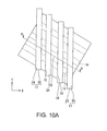
- FIG. 10A is a diagram illustrating a manufacturing step (step 8 ) of the memory cell array provided in the semiconductor device according to the embodiment of the invention and is a plan view of a region where the memory cell array is formed
- FIG. 10B is a cross-sectional view of the structure shown in FIG. 10A taken along the line A-A thereof;
- FIG. 11A is a diagram illustrating a manufacturing step (step 9 ) of the memory cell array provided in the semiconductor device according to the embodiment of the invention and is a plan view of a region where the memory cell array is formed,
- FIG. 11B is a cross-sectional view of the structure shown in FIG. 11A taken along the line A-A thereof;
- FIG. 12A is a diagram illustrating a manufacturing step (step 10 ) of the memory cell array provided in the semiconductor device according to the embodiment of the invention and is a plan view of a region where the memory cell array is formed
- FIG. 12B is a cross-sectional view of the structure shown in FIG. 12A taken along the line A-A thereof
- FIG. 12C is a cross-sectional view of the structure shown in FIG. 12A taken along the line B-B thereof;
- FIG. 13A is a diagram illustrating a manufacturing step (step 12 ) of the memory cell array provided in the semiconductor device according to the embodiment of the invention and is a cross-sectional view corresponding to the cross-section of FIG. 2A
- FIG. 13B is a cross-sectional view corresponding to the cross-section of FIG. 2B ;
- FIG. 14 is a plan view showing another example of a layout of a memory cell array applicable to a semiconductor device according to the embodiment of the invention.
- FIG. 15 is a plan view showing an example of a DRAM layout according to related art.
- FIG. 16 is a cross-sectional view of the DRAM shown in FIG. 15 taken along the line Z-Z thereof.
- the inventor obtained a new finding that as a DRAM (Dynamic Random Access Memory) memory cell is miniaturized, a distance between two adjacent cells provided in an active region is reduced, which will cause a disturb failure between the two adjacent cells (hereafter, referred to simply as the disturb failure) in which when one of the cells stores data “0” while the other stores data “1” and the cell storing data “0” is accessed successively, the data stored in the cell storing data “1” will be corrupted. This disturb failure will incur a risk of impairing the reliability of the semiconductor device.
- DRAM Dynamic Random Access Memory
- FIG. 15 is a plan view showing an example of a DRAM layout according to a related art
- FIG. 16 is a cross-sectional view of the DRAM shown in FIG. 15 , taken along the line Z-Z.
- a plurality of active regions 302 are provided on a surface of a semiconductor substrate 301 while being arranged in a regular manner.
- Each of the active regions 302 is surrounded by element isolation regions 303 formed by filling a trench formed on the surface of the semiconductor substrate 301 with an insulating film.
- a plurality of word lines WL are arranged to extend in a Y direction intersecting the active regions 302 .
- the word lines WL 1 , WL 2 are formed by being embedded in trenches via a gate insulating film 305 .
- the trenches are formed in the surface of the semiconductor substrate 301 to extend across the active regions 302 and element isolation regions 303 .
- a cap insulating film 306 is formed on top of each of the word lines WL 1 , WL 2 by being embedded in the trench.
- Each of the active regions 302 is provided with two word lines consisting of the word line WL 1 and the word line WL 2 which intersect with the active regions 302 .
- the two word lines WL 1 and WL 2 constitute gate electrodes of their corresponding two transistors Tr 1 and Tr 2 .
- the transistor Tr 1 is composed of a drain diffusion layer 307 and a source diffusion layer 308 as well as the gate electrode formed by the word line WL 1 .
- the transistor Tr 2 is composed of a drain diffusion layer 312 and the source diffusion layer 308 as well as the gate electrode formed by the word line WL 2 .
- the source diffusion layer 308 is common to the transistors Tr 1 and Tr 2 and is connected to a bit line BL at a bit line contact 311 .
- the drain diffusion layers 307 and 312 are respectively connected to lower electrodes 313 and 314 (storage nodes) via capacity contact plugs 310 formed in an interlayer insulating film 309 .
- the lower electrodes 313 and 314 respectively form capacity elements 316 and 317 together with a capacity insulating film and upper electrodes (not shown).
- the surfaces of the semiconductor substrate 301 corresponding to the bottom faces and opposing side faces of the trenches in which the word lines WL 1 and WL 2 are embedded serves as channels of the transistors Tr 1 and Tr 2 .
- the word line WL 1 when the word line WL 1 is turned on to form a channel of the transistor Tr 1 and a low (L) level potential is applied to the bit line 319 , the lower electrode 313 becomes L level. The word line WL 1 is then turn off whereby data of L level (data of “0”) is stored in the lower electrode 313 .
- the word line WL 2 for example is turn on to form a channel of the transistor Tr 2 and a high (H) level potential is applied to the bit line 319 , the lower electrode 314 becomes H level.
- the word line WL 2 is then turned off whereby data of H level (data of “1”) is stored in the lower electrode 314 .
- a state is established in which L-level data is stored in the lower electrode 313 and H level data is stored in the lower electrode 314 .
- the word line WL 1 corresponding to the L-side lower electrode 313 is repeatedly turned on and off (this operation corresponds to cell operation in other active regions using the same word line WL 1 ).
- adjacent cells must hold information independently from each other. However, if a disturb failure occurs in which the data storage state of one of the adjacent cells is changed due to operating state of the other cell, normal operation of the semiconductor device (DRAM) is impaired, leading to a problem of impaired reliability.
- DRAM semiconductor device
- This disturb failure does not occur as long as the cell size is large. For example, when the distance L between the word line WL 1 and the word line WL 2 defined by a minimum processing size F is 70 nm as shown in FIG. 15 , this disturb failure does not occur.
- FIG. 1 is a schematic plan view showing a memory cell array provided in a semiconductor device according to an embodiment of the invention.
- FIG. 2A is a cross-sectional view of the memory cell array shown in FIG. 1 , taken along the line A-A thereof.
- FIG. 2B is a cross-sectional view of the memory cell array shown in FIG. 1 , taken along the line B-B thereof.
- FIG. 2C is a perspective view for explaining a cross-sectional configuration of a fin provided in a gate electrode trench in the semiconductor device according to the embodiment.
- FIG. 2D is an enlarged cross-sectional view for explaining thickness of a gate insulating film provided in the semiconductor device according to the embodiment, and shows a cross-section taken along the line C-C in FIG. 1 .
- FIG. 2D shows only a fin 15 , a gate insulating film 21 , and a first element isolation region 14 , while the other components of a memory cell array 11 are omitted.
- FIG. 1 and FIGS. 2A to 2D a DRAM (Dynamic Random Access Memory) is used as an example of a semiconductor device 10 according to an embodiment of the invention.
- FIG. 1 illustrates an example of a layout of a DRAM memory cell array.
- the X direction represents a direction in which bit lines 34 extend
- the Y direction represents a direction (second direction) in which gate electrodes 22 and second element isolation regions 17 extend, intersecting with the X direction.
- FIG. 1 only shows a semiconductor substrate 13 , first element isolation regions 14 , active regions 16 , second element isolation regions 17 , gate electrode trenches 18 , gate electrodes 22 , bit lines 34 , capacity contact plugs 42 , capacity contact pads 44 , and a plurality of element formation regions R among the components of the memory cell array 11 , while the other components of the memory cell array 11 are omitted.
- FIG. 2A schematically shows bit lines 34 which actually extend in the X direction shown in FIG. 1 .
- FIGS. 2A to 2C like components to those of the semiconductor device 10 shown in FIG. 1 are indicated by the same reference numerals.
- the semiconductor device 10 has a memory cell region in which the memory cell array 11 shown in FIG. 1 and FIGS. 2A and 2B is formed, and a not-shown peripheral circuit region (a region where a peripheral circuit is formed) arranged around the memory cell region.
- the memory cell array 11 provided in the semiconductor device 10 has a semiconductor substrate 13 , a first element isolation region 14 , an active region 16 having a plurality of element formation regions R, a second element isolation region 17 , a gate electrode trench 18 , a fins 15 formed such that a part of the active region 16 protrudes from the bottom 18 c of the gate electrode trench 18 , a first and second transistor 19 - 1 , 19 - 2 , a gate insulating film 21 , a gate electrodes 22 which is an embedded gate electrode, an embedded insulating films 24 , a mask insulating film 26 , a first impurity diffusion region 28 , a second impurity diffusion region 29 , an opening 32 , a bit line contact plug 33 , a bit line 34 , a cap insulating film 36 , a sidewall film 37 , an interlayer insulating film 38 , a contact hole 41 , a capacity contact plug 42 ,
- the semiconductor substrate 13 is a plate-like substrate.
- the semiconductor substrate 13 may be, for example, a p-type mono-crystalline silicon substrate.
- the concentration of the p-type impurity in the semiconductor substrate 13 can be set to 1E16 atoms/cm 2 , for example.
- the first element isolation region 14 has a first element isolation trench 51 and a first element isolation insulating film 52 .
- the first element isolation trench 51 is formed in the semiconductor substrate 13 so as to extend in a direction (first direction) inclined at a predetermined angle to the X direction shown in FIG. 1 .
- the first element isolation trench 51 is formed in plurality at predetermined intervals with respect to the Y direction shown in FIG. 1 .
- the depth of the first element isolation trench 51 may be set to 250 nm, for example.
- the first element isolation insulating film 52 is provided so as to fill the first element isolation trench 51 . Although not shown in the drawings, the top face of the first element isolation insulating film 52 is made flush with the principal surface 13 a of the semiconductor substrate 13 .
- the first element isolation insulating film 52 may be, for example, a silicon oxide film (SiO 2 film).
- the first element isolation region 14 configured as described above defines an active region 16 extending in a band-like fashion across the second direction.
- the second element isolation region 17 has a second element isolation trench 54 and a second element isolation insulating film 55 .
- the second element isolation trench 54 is formed in the semiconductor substrate 13 so as to extend in the Y direction (second direction) as shown in FIG. 1 .
- the second element isolation trench 54 cuts off a part of the first element isolation region 14 .
- the second element isolation trenches 54 is formed in pair so as to sandwich the two gate electrodes 22 arranged adjacent to each other.
- Each of the gate electrodes 22 forms a word line of the memory cell. This means that in the memory cell according to this embodiment, one second element isolation region 17 and two gate electrodes 22 (word lines) extending in the Y direction constitute one set, which is arranged repeatedly in the X direction.
- the depth of the second element isolation trench 54 can be set to 250 nm, for example.
- the second element isolation insulating films 55 is formed to fill the second element isolation trench 54 and an opening 26 A formed in the mask insulating film 26 .
- the top face 55 a of the second element isolation insulating film 55 is flush with the top face 26 a of the mask insulating film 26 .
- the second element isolation insulating film 55 may be a silicon oxide film (SiO2 film), for example.
- the second element isolation regions 17 configured as described above defines a plurality of element formation regions R with respect to the second direction.
- the active region 16 is divided into a plurality of element formation regions R by providing the first element isolation region 14 formed by filling the first element isolation trench 51 formed in the semiconductor substrate 13 with the first element isolation insulating film 52 , and the second element isolation region 17 formed by filling the second element isolation trench 54 formed in the semiconductor substrate 13 with the second element isolation insulating film 55 .
- this configuration of the invention eliminates the risk of the first and second transistors 19 - 1 and 19 - 2 being adversely affected by potential of a dummy gate electrode, and hence makes it easy to turn the first and second transistors 19 - 1 and 19 - 2 on and off and improves the data holding performance memory cell array 11 .
- the gate electrode trench 18 is provided in pair in the semiconductor substrate 13 between two second element isolation regions 17 so as to extend in the Y direction.
- Each of the gate electrode trenches 18 is defined by the inner surfaces consisting of first and second side faces 18 a and 18 b facing each other and the bottom 18 c .
- the pair of gate electrode trenches 18 are arranged such that the second side faces 18 b face each other.
- each of the gate electrode trenches 18 is formed such that the depth of the bottom 18 c is smaller than the depth of the first and second element isolation trenches 51 and 54 (the depth of the first and second element isolation regions 14 and 17 ).
- the depth of the gate electrode trenches 18 is preferably set to 150 to 200 nm.
- the gate electrode trenches 18 are formed to extend across the first element isolation regions 14 and the active regions 16 . This means that each of the gate electrode trenches 18 is formed by a series of first trench sections 18 A formed in the active regions 16 and second trench sections 18 B formed in the first element isolation regions 14 .
- the bottom of the second trench section 18 B formed in the first element isolation region 14 constitutes the bottommost portion 18 c of the gate electrode trench 18 .
- each of the first trench section 18 A formed in the active region 16 has the same depth, at its ends facing the second trench sections 18 B, as the depth of the bottom of the second trench section 18 B.
- a fin 15 is formed in a central part of the first trench section 18 A such that a part of the active region 16 protrudes.
- the fin 15 has a top part 15 a and a pair of sides 15 b and 15 c facing each other.
- the top part 15 a extends in the direction where the active region 16 extends (first direction).
- the opposite ends in the extending direction of the top part 15 a are arranged in the first trench section 18 A to extend between the first side face 18 a and the second side face 18 b forming the gate electrode trench 18 .
- the pair of sides 15 b and 15 c are arranged to be in parallel with the direction in which the active region 16 extends (first direction).
- the fin 15 may have a sharp angular shape at the top as shown in FIGS. 2C and 2D , or may be more rounded at the top.
- the height of the fin 15 means, as indicated by the letter H in FIG. 2C , the height as measured vertically from the lowest point of the bottom 18 c of the gate electrode trench 18 to the point where the vertical line meets the top part 15 a.
- the height H of the fin 15 is preferably in a range of 10 to 40 nm.
- the top part 15 a of the fin 15 is preferably located at a position that is 100 nm or more deep from the surface of the semiconductor substrate 13 .
- the S factor (subthreshold factor) will be increased, leading to a problem of increased off-leakage current. In addition, this will reduce the current driving ability, leading to a problem of degraded write characteristics. If the height H of the fin 15 exceeds 40 nm, however, the disturb failure described above cannot be suppressed sufficiently.
- the height H of the fin 15 is within the abovementioned range, the increase of off-leakage current can be suppressed and the write characteristics can be improved while suppressing the disturb failure sufficiently.
- the first and second transistors 19 - 1 and 19 - 2 are trench-gate transistors, each having a gate insulating film 21 , a gate electrode 22 serving as an embedded word line of a saddle-fin type. an embedded insulating film 24 , a first impurity diffusion region 28 , and a second impurity diffusion region 29 .
- the first and second transistors 19 - 1 and 19 - 2 are arranged adjacent to each other.
- the second impurity diffusion region 29 functions as a common impurity diffusion region (drain region in the case of the structure as shown in FIGS. 2A and 2B ) for the first and second transistors 19 - 1 and 19 - 2 .
- the second side face 18 b of the gate electrode trench 18 forming the first transistor 19 - 1 and the second side face 18 b of the gate electrode trench 18 forming the second transistor 19 - 2 are arranged to face each other across the second impurity diffusion region 29 .
- the gate insulating film 21 is formed to cover the first and second side faces 18 a , 18 b of the gate electrode trenches 18 and the bottoms 18 c of the gate electrode trenches 18 .
- the gate insulating film 21 further covers the surfaces (i.e. the top part 15 a and the sides 15 b and 15 c facing each other) of the fin 15 provided on the bottom 18 c of each of the gate electrode trenches 18 .
- the gate insulating film 21 may be, for example, a single-layer silicon oxide film (SiO 2 film), a nitrided silicon oxide film (SiON film), a laminated silicon oxide film (SiO 2 film), or a laminated film having a silicon nitride film (SiN film) stacked on a silicon oxide film (SiO 2 film).
- the gate insulating film 21 can be formed to have an average thickness of 4 to 6 nm, for example.
- the inventor has newly found that when the potential of the gate electrode 22 (word line) is changed from on to off, it is difficult for electrons in the fin 15 to return to the diffusion layer serving as a source. If the electrons thus have been accumulated in the fin 15 , the electrons in the fin 15 may possibly reach the second impurity diffusion region 28 (drain region) forming the second transistor 19 - 2 to cause disturb failure, when the gate electrode 22 (word line) corresponding to the first transistor 19 - 1 is repeatedly turned on and off under previously established conditions in which L-level data is stored in the lower electrode 57 electrically connected to the first transistor 19 - 1 and H-level data is stored in the lower electrode 57 electrically connected to the second transistor 19 - 2 .
- the inventor further has found that the thickness distribution of the gate insulating film 21 can be controlled to control the flow of electrons when the potential of the gate electrode 22 (word line) is turned from on to off, so that migration of the electrons from the fin 15 to the diffusion layer serving as the source can be promoted and accumulation of electrons in the fin 15 can be prevented, resulting in increased operation speed and improved reliability of the transistors.
- the gate insulating film 21 has a relationship represented by t 1 >t 2 between a thickness t 1 of the first side face 18 a and second side face 18 b of the gate electrode trench 18 and a thickness t 2 of the top part 15 a of the fin 15 , it is difficult for electrons in the fin 15 to return to the diffusion layer serving as the source when the potential of the gate electrode 22 (word line) is changed from on to off.
- the amount of electrons in the channel is in an inverse correlation with the thickness of the gate insulating film 21 when the gate electrode 22 (word line) is on. Therefore, when it is assumed that the gate insulating film 21 has a relationship represented by t 1 >t 2 between a thickness t 1 of the first side face 18 a and second side face 18 b of the gate electrode trench 18 and a thickness t 2 of the top part 15 a of the fin 15 in a direction vertical to the surface of the semiconductor substrate 13 , many electrons will migrate into the fin 15 when the gate electrode 22 (word line) is on. Therefore, when the potential of the gate electrode 22 is changed from on to off, the amount of electrons to be transferred from the fin 15 to the diffusion layer serving as the source is increased.
- the time period required to stabilize the potential of the diffusion layer serving as the source is increased.
- it takes a long time to stabilize the potential of the diffusion layer serving as the source and hence the operation of the transistors is slow.
- the slow operation of the transistors causes impairment of reliability of the semiconductor device.
- a relationship represented by t 1 ⁇ t 2 is set between a thickness t 1 of the first side face 18 a and second side face 18 b of the gate electrode trench 18 shown in FIGS. 2A and 2B and a thickness t 2 of the top part 15 a of the fin 15 shown in FIG. 2D .
- the thicknesses t 1 and t 2 are in the relationship of t 1 ⁇ t 2 , the amount of electrons migrating to the fin 15 is suppressed when the gate electrode 22 (word line) is on, and hence the amount of electrons to be transferred from the fin 15 to the diffusion layer serving as the source is reduced when the potential of the gate electrode 22 is changed from on to off. Accordingly, the electrons in the fin 15 are allowed to return to the diffusion layer as the source in a short period of time and hence the potential of the diffusion layer as the source can be stabilized in a short period of time.
- the difference between t 1 and t 2 is preferably in the range of 0.5 to 3.0 nm.
- the difference between t 1 and t 2 is within the aforementioned range, the amount of electrons to be transferred from the fin 15 to the diffusion layer serving as the source can be effectively reduced, and the threshold voltage of the transistor can be easily set in a desirable range.
- t 1 can be set to 4.0 to 6.0 nm
- t 2 can be set to 4.5 to 7.0 nm.
- the disturb failure rate when the difference between t 1 and t 2 is null is normalized as 1
- the disturb failure rate is 0.8 when the difference between t 1 and t 2 is 0.5 nm
- the disturb failure rate is reduced as the difference between t 1 and t 2 becomes greater.
- the thickness t 3 of the bottoms of the sides 15 b and 15 c of the fin 15 means, as shown in FIG. 2D , a thickness t 3 as measured in a vertical direction to a normal line h 3 on the interface between the fin 15 and the gate insulating film 21 at a position shifted from the top part 15 a of the fin 15 toward the bottom 18 c of the gate electrode trench 18 by a distance corresponding to 90% of the height of the fin 15 (0.9h).
- the film thickness t 4 between t 2 and t 3 means a thickness as measured in a vertical direction to a normal line h 4 on the interface between the fin 15 and gate insulating film 21 at a position between t 2 and t 3 .
- a relationship represented by t 2 ⁇ t 4 ⁇ t 3 should be established among the thickness t 2 of the top part 15 a of the fin 15 , the thickness t 3 of the bottoms of the sides 15 b and 15 c of the fin 15 , and the film thickness t 4 between t 2 and t 3 .
- the relationship among t 2 , t 3 , and t 4 is t 2 ⁇ t 4 ⁇ t 3 , the migration of electrons from the bottoms of the sides 15 b and 15 c to the top part 15 a of the fin 15 is promoted when the potential of the gate electrode 22 (word line) is changed from on to off. Accordingly, the migration of electrons from the fin 15 to the diffusion layer serving as the source is facilitated, whereby the potential of the diffusion layer serving as the source can be stabilized in a short period of time and operation of the transistor is improved.
- the difference between t 4 and t 3 is preferably in a range of 0.5 to 3.0 nm.
- the film thickness t 4 between t 2 and t 3 is defined as a thickness t 4 as measured in a vertical direction to the normal line h 4 on the interface between the fin 15 and the gate insulating film 21 at a position shifted from the top part 15 a of the fin 15 toward the bottom 18 c of the gate electrode trench 18 by a distance corresponding to 50% of the height of the fin 15 (0.5h).
- t 4 can be set to a range of 4.5 to 6.0 nm
- t 3 can be set to a range of 5.0 to 7.5 nm.
- the operating speed is increased by about 2% when the difference between t 4 and t 3 is set to 1 nm, and is increased by about 5% when the difference between t 4 and t 3 is set to 2 nm.
- t 2 and t 4 are equally set to 6 nm, and the difference between t 4 and t 3 is set to 0.5 nm, 1 nm, and 2 nm by changing the size of t 3 , the operating speed is slightly increased in comparison with the case in which t 2 is set to 6 nm, and t 4 is set to 5.5 nm.
- the relationship between t 1 and t 2 of the gate insulating film 21 is t 1 ⁇ t 2 and the relationship among t 2 , t 3 , and t 4 is t 2 ⁇ t 4 ⁇ t 3 . Therefore, electrons in the fin 15 are allowed to easily return to the diffusion layer serving as the source when the potential of the gate electrode 22 (word line) is changed from on to off. This prevents the disturb failure caused by accumulation of electrons in the fin 15 .
- the embodiment of the invention can provide a highly reliable semiconductor device with transistors operating stably.
- the electrons in the fin 15 are allowed to easily return to the diffusion layer serving as the source when the potential of the gate electrode 22 (word line) is changed from on to off, and thus the disturb failure caused by accumulation of electrons in the fin 15 can be suppressed effectively.
- a saddle-fin type embedded word line is employed in the gate electrode 22 in order to reduce the off-leakage current and to improve the write characteristics. Employment of the saddle-fin type word line makes it possible to reduce the S factor, and hence the threshold voltage can be reduced while retaining the off-leakage current. Further, employment of the saddle-fin type word line makes it possible to improve the current driving ability, and hence the write characteristics can be improved.
- Each of the gate electrodes 22 is arranged to fill a lower part of the gate electrode trench 18 via the gate insulating film 21 .
- the gate electrode 22 is formed to stride over the fin 15 via the gate insulating film 21 .
- the top face 22 a of the gate electrode 22 is located at a lower level than the principal surface 13 a of the semiconductor substrate 13 .
- the gate electrode 22 can be formed, for example, in a laminated structure having a titanium nitride film and a tungsten film stacked sequentially.
- the threshold voltage of each of the first and second transistors 19 - 1 and 19 - 2 can be regulated as appropriate by adjusting the film thickness of the gate insulating film 21 and the work function of the gate electrode 22 .
- the threshold voltage should preferably be in a range of 0.5 to 1.0 V. If the threshold voltage is less than 0.5 V, the off-leakage current will be increased, leading to degradation of data retention characteristics.
- the threshold voltage exceeds 1.0 V, however, the current driving ability becomes so low that data writing cannot be done sufficiently, which also possibly leads to degradation of data retention characteristics.
- the threshold voltage of one or both of the first and second transistors 19 - 1 and 19 - 2 can be set to a range of 0.8 to 1.0 V by setting the average thickness of the gate insulating film 21 to a range of 4 to 6 nm (as calculated for a silicon oxide film) and setting the work function of the gate electrode 22 to a range of 4.6 to 4.8 eV.
- the embedded insulating film 24 is formed to cover the top face 22 a of the gate electrode 22 and to fill the gate electrode trench 18 having the gate insulating film 21 formed therein.
- the embedded insulating film 24 protrudes higher than the principal surface 13 a of the semiconductor substrate 13 , and the top face 24 a of this protruding portion is flush with the top face 26 a of the mask insulating film 26 .
- the embedded insulating film 24 may be a silicon oxide film (SiO 2 film).
- the mask insulating film 26 is formed on the top face 28 a of the first impurity diffusion region 28 .
- the mask insulating film 26 has a trench-like opening 26 A formed on the second element isolation trench 54 .
- the mask insulating film 26 functions as an etching mask when the second element isolation trench 54 is formed in the semiconductor substrate 13 by anisotropic etching.
- a silicon nitride film is used as the mask insulating film 26 .
- the thickness of the mask insulating film 26 can be 50 nm, for example.
- a first impurity diffusion region 28 is formed on a part of the semiconductor substrate 13 located on the side of the first side face 18 a to cover an upper part 21 A of the gate insulating film 21 formed on the first side face 18 a of the gate electrode trench 18 .
- first side face 18 a of the gate electrode trench 18 forming the first transistor 19 - 1 and the first side face 18 a of the gate electrode trench 18 forming the second transistor 19 - 2 respectively face the side faces of the second element isolation trenches 54 via the semiconductor substrate 13 .
- each of the first impurity diffusion region 28 is formed to include the top face 13 a of the semiconductor substrate 13 interposed between the first side face 18 a and the second element isolation trench 54 , and to cover the upper part 21 A of the gate insulating film 21 formed on the first side faces 18 a.
- the bottom face 28 b of the first impurity diffusion region 28 is located at a higher level than the top face 22 a of the gate electrode 22 embedded in the gate electrode trench 18 (at a position closer to the top face 13 a of the semiconductor substrate 13 ).
- the distance between a horizontal line including the bottom face 28 b of the first impurity diffusion region 28 and a horizontal line including the top face 22 a of the embedded gate electrode 22 is desirably in a range of 5 to 10 nm. If the distance is less than 5 nm, the junction field becomes so high and that the data retention characteristics will be degraded. In contrast, if the distance exceeds 10 nm, the current driving ability will be reduced, also leading to degradation of write characteristic.
- the first impurity diffusion region 28 is provided in each of the gate electrodes 22 forming the first and second transistors 19 - 1 and 19 - 2 .
- the first impurity diffusion regions 28 are impurity diffusion regions functioning as source/drain regions (source regions in case of the configuration shown in FIGS. 2A and 2B ) of the first and second transistors 19 - 1 and 19 - 2 .
- the semiconductor substrate 13 is a p-type silicon substrate
- the second impurity diffusion region 29 is formed in a part of the semiconductor substrate 13 between the two gate electrode trenches 18 . More specifically, the second impurity diffusion region is formed such that the second impurity diffusion region 29 is shallower than the bottom 18 c of the gate electrode trench 18 and deeper than the apex of the fin 15 (the part of the top face 15 a closest to the surface 13 a of the semiconductor substrate 13 ). This means that the bottom of the second impurity diffusion region 29 is located at a level between the apex of the top face 15 a of the fin 15 and the bottom 18 c of the gate electrode trench 18 . In other words, the position of junction between the second impurity diffusion region 29 (e.g.
- n-type diffusion region and the semiconductor substrate 13 (e.g. p-type channel) is located in a range between the lower limit of depth defined by the apex of the fin 15 and the upper limit of depth defined by the bottom 18 c of the gate electrode trench 18 .
- the second impurity diffusion region 29 is arranged to cover the entire gate insulating films 21 formed on the second side faces 18 b of the two gate electrode trenches 18 except their lower ends.
- the doped impurity e.g. n-type impurity
- the doped impurity will reach the fin 15 , and hence the resulting voltage will be lower than a desired threshold voltage (Vt).
- the channel concentration e.g. concentration of p-type impurity
- the second impurity diffusion region 29 is an impurity diffusion region functioning as a common source/drain region (drain region in the case of the configuration shown in FIG. 2 ) for the first and second transistors 19 - 1 and 19 - 2 .
- the semiconductor substrate 13 is a p-type silicon substrate
- the second impurity diffusion region 29 is formed by implanting an n-type impurity ion into the semiconductor substrate 13 .
- the semiconductor device 10 is provided with the first impurity diffusion region 28 and the second impurity diffusion region 29 .
- the first impurity diffusion region 28 has the fins 15 formed at the bottoms 18 c of the gate electrode trenches 18 , includes the top face 13 a of the semiconductor substrate 13 interposed between the first side face 18 a and the second element isolation trench 54 , and covers the upper part 21 A of the gate insulating film 21 formed on the first side face 18 .
- the second impurity diffusion region 29 is arranged in a part of the semiconductor substrate 13 located between the two gate electrode trenches 18 , and covers the entire of the gate insulating film 21 formed on the second side faces 18 b of the gate electrode trenches 18 except their lower ends.
- a first channel region is formed in the fins 15 while a second channel region is formed in the semiconductor substrate 13 in contact with the lower part of the gate insulating film 21 formed on the first side face 18 a , in the semiconductor substrate 13 in contact with the bottoms 18 c of the gate electrode trenches 18 , and in the semiconductor substrate 13 located at a lower level than the bottom of the second impurity diffusion region 29 formed on the second side face 18 b .
- no channel region is formed in the part of the semiconductor substrate 13 that is in contact with the second side face 18 b and located at an upper level than the bottom the second impurity diffusion region 29 .
- the fins 15 which are completely depleted shows lower resistance than related transistors and allows electric current to flow therethrough more easily. This makes it possible to reduce the channel resistance and increase the on current even in miniaturized memory cells.
- the first and second transistors 19 - 1 and 19 - 2 are allowed to operate independently and stably.
- the fin 15 is formed in the bottom 18 c of each of the two gate electrode trenches 18 adjacent to each other such that the height H of the fin 15 is 40 nm or less.
- the gate electrode 22 (word line) corresponding to the first transistor 19 - 1 is repeatedly turned on and off in the state in which L-data is stored in the lower electrode 57 electrically connected to the first transistor 19 - 1 while H-data is stored in the lower electrode 57 electrically connected to the second transistor 19 - 2 , electrons e-generated in the channel of the first transistor 19 - 1 can be prevented from reaching the second impurity diffusion region 28 (drain region) forming the second transistor 19 - 2 .
- the electrons e ⁇ generated in the channel of the first transistor 19 - 1 will not corrupt the H-level data stored in the lower electrode 5 electrically connected to the second transistor 19 - 2 and change it to L-level data. Accordingly, the occurrence of disturb failure can be prevented in which the stored data in one of the adjacent cells is changed due to an operation state of the other cell.
- the occurrence of the disturb failure can be prevented even in a DRAM in which the distance between two adjacent gate electrodes 22 is 50 nm or less.
- the opening 32 is formed between the embedded insulating films 24 protruding from the two gate electrode trenches 18 .
- the opening 32 is formed so as to expose the top face 29 a of the second impurity diffusion region 29 .
- a bit line contact plug 33 is formed to fill the opening 32 and formed integrally with the bit line 34 .
- the lower end of the bit line contact plug 33 is in contact with the top face 29 a of the second impurity diffusion region 29 .
- the bit line 34 is formed of a laminated film formed by sequentially stacking a polysilicon film, a titanium nitride (TiN) film and a tungsten (W) film
- the bit line contact plug 33 can be formed of a polysilicon film.
- the bit line 34 is provided on the top face 24 a of the embedded insulating film 24 and is formed integrally with the bit line contact plug 33 .
- the bit line 34 is electrically connected to the second impurity diffusion region 29 via the bit line contact plug 33 .
- the bit line 34 can be formed of a laminated film composed a polysilicon film, a titanium nitride film and a tungsten film sequentially stacked, a polysilicon film, a titanium nitride film, or the like.
- the cap insulating film 36 is formed to cover the top face of the bit line 34 .
- the cap insulating film 36 not only protects the top face of the bit line 34 but also functions as an etching mask when a base material for the bit line 34 is patterned by anisotropic etching (specifically, by drying etching).
- the cap insulating film 36 may be a silicon nitride film (SiN film).
- the sidewall film 37 is formed to cover each side face of the bit line 34 .
- the sidewall film 37 has a function to protect the side walls of the bit line 34 .
- the sidewall film 37 may be a laminated film composed of a silicon nitride film (SiN film) and a silicon oxide film (SiO2 film) sequentially stacked.
- the interlayer insulating film 38 is formed on the top face 26 a of the mask insulating film 26 and on the top face 55 a of the second element isolation insulating film 55 .
- the top face 38 a of the interlayer insulating film 38 is flush with the top face 36 of the cap insulating film 36 .
- the interlayer insulating film 38 may be, for example, a silicon oxide film (SiO 2 film) formed by a CVD method, or a coat-type insulating film (silicon oxide film (SiO 2 film)) formed by a SOG (Spin on Glass) method.
- the contact hole 41 is formed in the embedded insulating film 24 , the mask insulating film 26 , and the interlayer insulating film 38 so as to expose part of the top face 28 a of the first impurity diffusion region 28 .
- the capacity contact plug 42 is formed to fill the contact hole 41 .
- the lower end of the capacity contact plug 42 is in contact with a part of the top face 28 a of the first impurity diffusion region 28 .
- the capacity contact plug 42 is electrically connected to the first impurity diffusion region 28 .
- the top face 42 a of the capacity contact plug 42 is flush with the top face 38 a of the interlayer insulating film 38 .
- the capacity contact plug 42 may be of a laminated structure consisting, for example, of a titanium nitride film and a tungsten film sequentially stacked.
- the capacity contact pad 44 is formed on the top face 38 a of the interlayer insulating film 38 such that a part of the capacity contact pad 44 is connected to the top face 42 a of the capacity contact plug 42 .
- the lower electrode 57 forming the capacitor 48 is connected onto the capacity contact pad 44 .
- the capacity contact pad 44 electrically connects the capacity contact plug 42 and the lower electrode 57 .
- the capacity contact pads 44 are of a circular shape and are arranged in a staggered fashion with respect to the capacity contact plugs 42 which are aligned in the Y direction. These capacity contact pads 44 are each arranged between adjacent bit lines 34 in the X direction.
- the capacity contact pads 44 are arranged in a staggered fashion such that the centers of the alternate capacity contact pads 44 are arranged on the gate electrodes 22 along Y direction, or such that the centers of the alternate capacity contact pads 44 are arranged above the side faces of the gate electrodes 22 along Y direction. In other words, the capacity contact pads 44 are arranged in a zigzag manner in the Y direction.
- the silicon nitride film 46 is formed on the top face 38 a of the interlayer insulating film 38 so as to surround the periphery of the capacity contact pad 44 .
- One capacitor 48 is provided on each of the capacity contact pads 44 .
- Each of the capacitors 48 has one lower electrode 57 , a capacity insulating film 58 common for a plurality of lower electrodes 57 , and an upper electrode 59 common for a plurality of lower electrode 57 .
- the lower electrode 57 is formed on the capacity contact pad 44 and connected to the capacity contact pad 44 .
- the lower electrode 57 is of a crown shape.
- the capacity insulating film 58 is formed to cover the surfaces of the plurality of lower electrodes 57 exposed from the silicon nitride film 46 and the top face of the silicon nitride film 46 .
- the upper electrode 59 is formed to cover the surface of the capacity insulating film 58 .
- the upper electrode 59 is arranged to fill the inside of each lower electrode 57 having the capacity insulating film 58 formed thereon, and the space between the lower electrodes 57 .
- the top face 59 a of the upper electrode 59 is located at a higher level than the upper ends of the lower electrodes 57 .
- the capacitor 48 configured as described above is electrically connected to the first impurity diffusion region 28 via the capacity contact pad 44 .
- interlayer insulating film (not shown) covering the top face 59 a of the upper electrode 59 , a contact plug (not shown) formed within the interlayer insulating film, and wiring (not shown) connected to the contact plug.
- the semiconductor device 10 has a configuration as described below.
- the semiconductor device 10 includes a plurality of first element isolation regions 14 formed of a semiconductor substrate 13 and formed in the semiconductor substrate 13 so as to extend in a first direction and each defining an active region 16 having a plurality of element formation regions R; a plurality of second element isolation regions 17 formed in the semiconductor substrate 13 so as to extend in a second direction intersecting with the first direction and defining each of the active regions 16 into a plurality of element formation regions R; a pair of gate electrode trenches 18 formed in a surface layer of the semiconductor substrate 13 between the adjacent second element isolation regions 17 and 17 so as to extend in the second direction intersecting with the first element isolation regions 14 and the active regions 16 , and having first and second side faces 18 a and 18 b facing each other and the bottom 18 c ; fins 15 each formed such that a part of the active region 16 protrudes from the bottom 18 c of the gate electrode trench 18 by forming the gate electrode trench 18 such that second trench section 18 B of the gate
- the element formation regions R share the second impurity diffusion region 29 .
- the semiconductor device 10 has a first transistor 19 - 1 which is composed, at least, of one of the gate electrodes 22 , one of the fins 15 and one of the first impurity diffusion regions 28 , and a second transistor 19 - 2 which is composed, at least, of the other gate electrode 22 and fin 15 and the first impurity diffusion region 28 .
- the second impurity diffusion region 29 is formed to be shallower than the bottoms 18 c of the gate electrode trenches 18 and deeper than the apexes (tops) of the fins 15 .
- the semiconductor device 10 is configured such that a fin 15 is provided at the bottom 18 c of each of the gate electrode trenches 18 , while the semiconductor device 10 is provided with the first impurity diffusion regions 28 including the top face 13 a of the semiconductor substrate 13 between the first side faces 18 a and the second element isolation trenches 54 , and covering the upper parts 21 A of the gate insulating films 21 arranged on the first side faces 18 a , and the second impurity diffusion region 29 arranged at a part of the semiconductor substrate 13 sandwiched between the two gate electrode trenches 18 and covering the entire of the gate insulating film 21 arranged on the second side faces 18 b of the pair of gate electrode trenches 18 except lower parts of the gate insulating film 21 .
- the semiconductor device 10 is configured such that, when the first and second transistors 19 - 1 and 19 - 2 operate, the first channel region is formed in the fin 15 , while the second channel region is formed in a part of the semiconductor substrate 13 in contact with the lower parts of the gate insulating films 21 formed on the first side faces 18 a , in a part of the semiconductor substrate 13 in contact with the bottom faces 18 c of the gate electrode trenches 18 , and in a part of the semiconductor substrate 13 located at a lower level than the bottom of the second impurity diffusion region 29 arranged on the second side faces 18 b , whereas no channel region is provided in the part of the semiconductor substrate 13 that is in contact with the second side faces 18 b and located at a higher level than the bottom of the second impurity diffusion region 29 .
- a manufacturing method of the semiconductor device 10 (more specifically, the memory cell array 11 ) of this embodiment will be described with reference to FIG. 3 to FIG. 14 .
- figure numbers with suffix “A” each represent a front view.
- Those figure numbers with suffix “B” are cross-sectional views taken along the line A-A in FIG. 1
- those with suffix “C” are cross-sectional views taken along the line B-B in FIG. 1
- those with suffix “D” are cross-sectional views taken along the line C-C in FIG. 1 .
- any redundant drawings relating to the same structure will be omitted.
- FIG. 3B is the same as FIG. 3C
- FIG. 3C is omitted.
- the cross-sectional view taken along the line C-C shows a cross-section taken along a direction in which the gate electrode 22 serving as an embedded word line of the semiconductor device 10 according to the embodiment.
- a pad oxide film 65 is formed on the principal surface 13 a of the semiconductor substrate 13 . Subsequently, a silicon nitride film 66 having trench-like openings 66 a is formed on the pad oxide film 65 .
- the opening 66 a extends in a strip-like fashion in a direction inclined at a predetermined angle (first direction) relative to the X direction, and is formed in plurality at predetermined intervals in the Y direction.
- the semiconductor substrate 13 is etched by anisotropic etching, using the silicon nitride film 66 having the openings 66 a as a mask, so that first element isolation trenches 51 extending in the first direction are formed.
- the first element isolation trench 51 may have a width W 1 of 43 nm, for example.
- a depth D 1 of the first element isolation trenches 51 (a depth as measured from the principal surface 13 a of the semiconductor substrate 13 ) may be 250 nm, for example.
- a first element isolation insulating film 52 is formed to fill the first element isolation trenches 51 .
- the first element isolation trenches 51 are filled with a silicon oxide film (SiO 2 film) formed by a HDP (High Density Plasma) method or SOG (Spin on Glass) method.
- SiO 2 film silicon oxide film formed by a HDP (High Density Plasma) method or SOG (Spin on Glass) method.
- Parts of the silicon oxide film (SiO 2 film) present on and protruding over the top face of the silicon nitride film 66 are removed by a CMP (Chemical Mechanical Polishing) method, whereby the first element isolation insulating films 52 are formed in the first element isolation trenches 51 .
- CMP Chemical Mechanical Polishing
- first element isolation regions 14 are formed, each consisting of the first element isolation trench 51 and the first element isolation insulating film 52 and defining a strip-like active region 16 extending in the first direction.
- the silicon nitride film 66 shown in FIG. 4D is removed, and then the pad oxide film 65 is removed by wet etching.
- the top face 52 a of the first element isolation insulating film 52 is made flush with the principal surface 13 a of the semiconductor substrate 13 by removing the parts projecting above the principal surface 13 a of the semiconductor substrate.
- a mask insulating film 26 formed of a silicon nitride film having a trench-like opening 26 A is formed on the principal surface 13 a of the semiconductor substrate 13 and the top face 52 a of the first element isolation insulating film 52 shown in FIG. 5D .
- the opening 26 A extends in the Y direction (second direction) and formed in plurality at predetermined intervals with respect to the X direction (see FIG. 6A ).
- the openings 26 A is formed to expose parts of the principal surface 13 a of the semiconductor substrate 13 corresponding to regions where second element isolation trenches 54 are formed.
- the second element isolation trenches 54 extending in the first direction are formed by anisotropically dry etching the semiconductor substrate 13 , using the mask insulating film 26 having the openings 26 A as a mask.
- a depth D 2 of the second element isolation trenches 54 (as measured from the principal surface 13 a of the semiconductor substrate 13 ) may be 250 nm, for example.
- the second element isolation trenches 54 may be formed by simultaneously etching the first element isolation insulating film 52 adjacent to the semiconductor substrate 13 .
- a second element isolation insulating film 55 formed of a silicon oxide film is formed to fill the second element isolation trenches 54 s.
- a part of the insulating film protruding above the top face 26 a of the mask insulating film 26 is removed by a CMP method, whereby second element isolation trenches 54 are filled, and a second element isolation insulating film 55 having a top face 55 a flush with the top face 26 a of the mask insulating film 26 is formed.
- the second element isolation regions 17 are formed, each consisting of the second element isolation trench 54 and the second element isolation insulating film 55 and defining a strip-like active region 16 into a plurality of element formation regions R shown in FIG. 3A .
- two trench-like openings 26 B extending in the Y direction are formed in the mask insulating film 26 located between the two second element isolation regions 17 .
- the element isolation insulating film 52 forming the first element isolation regions 14 is selectively etched by anisotropic dry etching, using the mask insulating film 26 having the openings 26 B as a mask, whereby a second trench section 18 B of a gate electrode trench 18 is formed in each of the first element isolation regions 14 .
- the second trench section 18 B should be formed such that the depth D 4 thereof (the depth as measured from the principal surface 13 a of the semiconductor substrate 13 , not shown) is smaller than depths D 1 and D 2 of the first and second element isolation trenches 51 and 54 .
- the depth D 4 may be in a range of 150 to 200 nm.
- the semiconductor substrate 13 forming the active regions 16 is then selectively etched.
- a first trench section 18 A of the gate electrode trench 18 is formed in the active region 16 , and such that the depth D 3 of the first trench section 18 A (the depth as measured from the principal surface 13 a of the semiconductor substrate 13 ) is smaller than the depth D 4 of the second trench section 18 B.
- the first trench section 18 A should be formed such that depth D 3 thereof is smaller than the depth D 4 of the second trench section 18 B by 10 to 40 nm.
- the depth D 4 of the gate electrode trench 18 may be 150 nm, for example.
- selective anisotropic etching is performed using the mask insulating film 26 having the openings 26 B as a mask until the depth of a part of the first trench section 18 A forming the gate electrode trench 18 and facing the second trench section 18 B becomes substantially the same as the depth of the second trench section 18 B.
- the first trench section 18 A of the gate electrode trench 18 that is formed in the active region 16 can be formed such that the depth at the ends thereof facing the second trench section 18 B is the same as the depth of the second trench section 18 B (i.e. the depth D 4 ) (see FIGS. 8C and 8D ), and such that a central part of the first trench section 18 A has the depth D 3 (see FIGS. 8B and 8D ).
- the gate electrode trenches 18 each having the first and second side faces 18 a and 18 b and the bottom 18 c can be formed, and each of the fins 15 can be formed such that a part of the active region 16 protrudes from the bottom 18 c.
- a gate insulating film 21 is formed to cover the surfaces of the gate electrode trenches 18 (i.e. the first and second side faces 18 a and 18 b , and the bottom faces 18 c of the gate electrode trenches 18 ) and the surfaces of the fins 15 (i.e. the top part 15 a and a pair of side faces 15 b and 15 c facing each other of each fin 15 ).
- the gate insulating film 21 may be, for example, a single-layer silicon oxide film (SiO 2 film), a nitrided silicon oxide film (SiON film), a laminated silicon oxide film (SiO 2 film), and a laminated film having a silicon nitride film (SiN film) stacked on a silicon oxide film (SiO 2 film).
- the formation of the gate insulating film 21 having controlled thickness distribution can be realized, for example, by a method using a low-energy plasma oxidation processing apparatus capable of applying a bias voltage by RF power control.
- Plasma oxidation processing can be performed, for example, under conditions in which temperature is set in a range of 400 to 600° C., pressure is set in a range of 10 to 200 Pa, an Ar-based gas mixture with an oxygen partial pressure of 0.5 to 5% is used, and RF power is set in a range of 0.1 to 1 kW.
- the pressure in a range of 10 to 30 Pa, the oxygen partial pressure in a range of 0.5 to 1.5%, and the RF power in a range of 0.5 to 0.7 kW.
- the gate insulating film 21 can be obtained to satisfy the conditions that the relationship between the thickness t 1 of the first side faces 18 a and second side faces 18 b of the gate electrode trenches 18 and the thickness t 2 of the top parts 15 a of the fins 15 is represented by t 1 ⁇ t 2 and/or the relationship among the thickness t 2 , the thickness t 3 of the bottoms of the side faces 15 b and 15 c of the fins 15 , and a film thickness t 4 between t 2 and t 3 is represented by t 2 ⁇ t 4 ⁇ t 3 .
- gate electrodes 22 are formed to fill the lower parts of the gate electrode trenches 18 via the gate insulating film 21 so as to stride over the fins 15 , such that the top faces 22 a of the gate electrodes 22 are lower than the principal surface 13 a of the semiconductor substrate 13 (see FIG. 9D ).
- the gate electrodes 22 are formed by sequentially stacking a titanium nitride film and a tungsten film by a CVD method, for example, and then totally etching back the titanium nitride film and the tungsten film. Each of the gate electrodes 22 forms a word line of memory cells.
- an embedded insulating film 24 formed of a silicon nitride film is formed to cover the top faces 22 a of the gate electrodes 22 and to fill the gate electrode trenches 18 and the trench-like openings 26 B.
- the embedded insulating film 24 has a top face 24 a flush with the top face 26 a of the mask insulating film 26 .
- phosphorus (P) ion as a n-type impurity is implanted into the entire top face of the structure shown in FIGS. 9B and 9C under the conditions of energy of 100 KeV and a dose amount of 1E14 atoms/cm 2 , whereby first impurity diffusion regions 28 are formed in the semiconductor substrate 13 between the gate electrode trenches 18 and the first element isolation regions 17 , while an impurity diffusion region 71 constituting a part of the second impurity diffusion region 29 is formed in the semiconductor substrate 13 present the two gate electrode trenches 18 .
- the first impurity diffusion regions 28 are formed in the parts of the semiconductor substrate 13 present on the sides of the first side faces 18 a of the gate electrode trenches 18 so as to cover the upper parts 21 A of the gate insulating films 21 formed on the first side faces 18 a.
- the first impurity diffusion regions 28 are each formed to include the top face 13 a of the part of the semiconductor substrate 13 interposed between the first side face 18 a and the second element isolation trench 54 and to have its bottom face 28 b at a higher level than the top faces 22 a of the gate electrodes 22 .
- the formation of the first impurity diffusion regions 28 need not necessarily be performed in this step, but may be performed in the step shown in FIG. 4 or FIG. 5 , for example.
- a mask film 73 having a trench-like opening 73 a exposing the top face 26 a of the mask insulating film 26 present between the embedded insulating films 24 is formed on the top faces 24 a of the embedded insulating films 24 , the top face 26 a of the mask insulating film 26 , and the top faces 55 a of the second element isolation insulating films 55 .
- the mask insulating film 26 exposed from the opening 73 a is removed by anisotropic dry etching, using the mask film 73 as a mask.
- An opening 32 is formed by the removal of the mask insulating film 26 .
- the top face 71 a of the impurity diffusion region 71 is exposed and a part of the top face 52 of the first element isolation insulating film 52 flush with the top face 71 a of the impurity diffusion region 71 is exposed.
- phosphorus (P) ion as an n-type impurity is selectively implanted in the impurity diffusion region 71 exposed from the mask film 73 (in other words, in the part of the semiconductor substrate 13 where the impurity diffusion region 71 is formed), whereby a second impurity diffusion region 29 is formed in a part of the semiconductor substrate 13 located between the two gate electrode trenches 18 such that the bottom of the second impurity diffusion region 29 is located at a level between the apexes of the top faces 15 a of the fins 15 and the bottoms 18 c of the gate electrode trenches 18 .
- the ion implantation is performed in two steps.
- the ion implantation is performed under the conditions of energy of 15 KeV and a dose amount of 5E14 atoms/cm 2
- the ion implantation is performed under the conditions of energy of 30 KeV, and a dose amount of 2E13 atoms/cm 2 .
- the second impurity diffusion region 29 is formed to cover the entire of the gate insulating films 21 formed on the second side faces 18 b of the two gate electrode trenches 18 , except the lower ends of the gate insulating films 21 , and first and second transistors 19 - 1 and 19 - 2 each having the gate insulating film 21 , the fin 15 , the gate electrode 22 , the embedded insulating film 24 , the first impurity diffusion region 28 , and the second impurity diffusion region 29 are formed.
- the mask film 73 is then removed.
- bit line contact plugs 33 for filling the openings 32 , and bit lines 34 arranged on the bit line contact plugs 33 and extending in the X direction (see FIG. 1 ) are formed collectively.
- the opening 32 is filled with a phosphorus-doped silicon film to form a bit line contact plug 33 .
- the bit line contact plug 33 is separated in the second direction.
- a titanium nitride film, a tungsten film, and a cap insulating film 36 are sequentially formed on the top face 24 a of the embedded insulating film 24 .
- a mask film for forming a bit line pattern is formed on the cap insulating film 36 .
- the cap insulating film 36 , the tungsten film, the titanium nitride film, and the phosphorus-doped silicon film are patterned by anisotropic dry etching using the mask film as a mask, so that bit line contact plugs 33 separated in the second direction and bit lines 34 formed on the bit line contact plugs 33 and consisting of a titanium nitride film and a tungsten film are formed collectively.
- sidewall films 37 each consisting of a silicon nitride film (SiN film) and a silicon oxide film (SiO 2 film) which are not shown are formed to cover the side faces of the bit lines 34 and the cap insulating film 36 .
- an interlayer insulating film 38 having the top face 38 a flush with the top face 36 a of the cap insulating film 36 is formed on the entire surface.
- the interlayer insulating film 38 , the mask insulating film 26 , the embedded insulating film 24 , and the gate insulating film 21 are anisotropically dry etched, so that capacity contact holes 41 exposing a part of the top faces 28 a of the first impurity diffusion regions 28 are formed.
- a titanium nitride film and a tungsten film are sequentially formed by a CVD method so as to fill the capacity contact holes 41 .
- undesired parts of the titanium nitride film and tungsten film formed on the top face 38 a of the interlayer insulating film 38 are removed by polishing using a CMP method, so that the capacity contact plugs 42 are formed.
- formation of the capacity contact pads 44 , formation of the silicon nitride film 46 , and formation of the capacitors 48 each consisting of a lower electrode 57 , a capacity insulating film 58 , and an upper electrode 59 are performed, whereby the semiconductor device 10 according to the embodiment is manufactured.
- the present invention is not limited to the above embodiments, but may be modified and changed without departing from the scope and spirit of the invention.
- the above embodiments have been described using an example of a semiconductor device represented by a DRAM. Nevertheless, the present invention is applicable to any other semiconductor devices.
- the number and size of pads arranged are not limited to the illustrated examples and may be set in any desired manner.
- FIG. 14 is a plan view showing another example of a memory cell array layout which is applicable to the semiconductor device according to the embodiment of the invention.
- like components as those of the structure shown in FIG. 1 are indicated by the same reference numerals.
- the semiconductor device 10 according to the embodiment as described above is also applicable to the layout as shown in FIG. 14 in which active regions 16 and bit lines 34 are formed in a zigzag pattern.
- the invention is applicable to a semiconductor device and a manufacturing method thereof.
Abstract
Description
Claims (13)
Priority Applications (1)
| Application Number | Priority Date | Filing Date | Title |
|---|---|---|---|
| US14/186,369 US9236387B2 (en) | 2012-01-17 | 2014-02-21 | Semiconductor device and manufacturing method thereof |
Applications Claiming Priority (2)
| Application Number | Priority Date | Filing Date | Title |
|---|---|---|---|
| JP2012007445A JP2013149686A (en) | 2012-01-17 | 2012-01-17 | Semiconductor device |
| JP2012-007445 | 2012-01-17 |
Related Child Applications (1)
| Application Number | Title | Priority Date | Filing Date |
|---|---|---|---|
| US14/186,369 Continuation US9236387B2 (en) | 2012-01-17 | 2014-02-21 | Semiconductor device and manufacturing method thereof |
Publications (2)
| Publication Number | Publication Date |
|---|---|
| US20130181271A1 US20130181271A1 (en) | 2013-07-18 |
| US8704299B2 true US8704299B2 (en) | 2014-04-22 |
Family
ID=48779388
Family Applications (2)
| Application Number | Title | Priority Date | Filing Date |
|---|---|---|---|
| US13/736,381 Expired - Fee Related US8704299B2 (en) | 2012-01-17 | 2013-01-08 | Semiconductor device and manufacturing method thereof |
| US14/186,369 Active 2033-01-11 US9236387B2 (en) | 2012-01-17 | 2014-02-21 | Semiconductor device and manufacturing method thereof |
Family Applications After (1)
| Application Number | Title | Priority Date | Filing Date |
|---|---|---|---|
| US14/186,369 Active 2033-01-11 US9236387B2 (en) | 2012-01-17 | 2014-02-21 | Semiconductor device and manufacturing method thereof |
Country Status (2)
| Country | Link |
|---|---|
| US (2) | US8704299B2 (en) |
| JP (1) | JP2013149686A (en) |
Cited By (2)
| Publication number | Priority date | Publication date | Assignee | Title |
|---|---|---|---|---|
| US20160099248A1 (en) * | 2013-05-16 | 2016-04-07 | Ps5 Luxco S.A.R.L. | Semiconductor memory device with improved active area/word line layout |
| US10573654B2 (en) * | 2018-06-18 | 2020-02-25 | Micron Technology, Inc. | Integrated assemblies having bitline contacts |
Families Citing this family (11)
| Publication number | Priority date | Publication date | Assignee | Title |
|---|---|---|---|---|
| JP2012234964A (en) | 2011-04-28 | 2012-11-29 | Elpida Memory Inc | Semiconductor device and manufacturing method of the same |
| JP2014022388A (en) * | 2012-07-12 | 2014-02-03 | Ps4 Luxco S A R L | Semiconductor device and method for manufacturing the same |
| KR102057073B1 (en) * | 2013-07-26 | 2019-12-18 | 에스케이하이닉스 주식회사 | Semiconductor device with bit line structure in a trench, and package, module and system including the same |
| US9171847B1 (en) * | 2014-10-02 | 2015-10-27 | Inotera Memories, Inc. | Semiconductor structure |
| KR102552949B1 (en) * | 2016-09-02 | 2023-07-06 | 삼성전자주식회사 | Semiconductor device |
| CN109216358B (en) * | 2017-07-03 | 2021-04-30 | 华邦电子股份有限公司 | Semiconductor structure and manufacturing method thereof |
| US10636796B2 (en) * | 2017-08-02 | 2020-04-28 | Winbond Electronics Corp. | Dynamic random access memory and method of fabricating the same |
| KR102403031B1 (en) * | 2017-10-19 | 2022-05-27 | 삼성전자주식회사 | Semiconductor devices |
| KR20210047125A (en) | 2019-10-21 | 2021-04-29 | 삼성전자주식회사 | Semiconductor memory devices |
| CN113764341B (en) * | 2020-06-05 | 2023-09-19 | 长鑫存储技术有限公司 | Semiconductor structure, manufacturing method thereof and semiconductor memory |
| CN116568031B (en) * | 2023-07-12 | 2023-11-17 | 长鑫存储技术有限公司 | Semiconductor structure and preparation method thereof |
Citations (4)
| Publication number | Priority date | Publication date | Assignee | Title |
|---|---|---|---|---|
| US6501119B1 (en) * | 1998-11-24 | 2002-12-31 | Sony Corporation | Semiconductor memory device and method of producing same |
| US20060273388A1 (en) | 2005-06-03 | 2006-12-07 | Elpida Memory, Inc. | Semiconductor device and method for manufacturing the same |
| JP2007081095A (en) | 2005-09-14 | 2007-03-29 | Elpida Memory Inc | Method of manufacturing semiconductor device |
| US7622354B2 (en) * | 2007-08-31 | 2009-11-24 | Qimonda Ag | Integrated circuit and method of manufacturing an integrated circuit |
Family Cites Families (8)
| Publication number | Priority date | Publication date | Assignee | Title |
|---|---|---|---|---|
| JP4246929B2 (en) * | 2001-06-29 | 2009-04-02 | 株式会社東芝 | Semiconductor memory device and manufacturing method thereof |
| JP2006054431A (en) * | 2004-06-29 | 2006-02-23 | Infineon Technologies Ag | Transistor, memory cell array, and manufacturing method of the transistor |
| KR100618875B1 (en) * | 2004-11-08 | 2006-09-04 | 삼성전자주식회사 | Semiconductor memory device having vertical channel MOS transistor and method for manufacturing the same |
| JP2008053274A (en) * | 2006-08-22 | 2008-03-06 | Elpida Memory Inc | Semiconductor device and its manufacturing method |
| JP2009088188A (en) * | 2007-09-28 | 2009-04-23 | Sanyo Electric Co Ltd | Trench gate type transistor and method for manufacturing same |
| WO2011039800A1 (en) * | 2009-09-29 | 2011-04-07 | 株式会社 東芝 | Semiconductor device |
| JP2011138883A (en) * | 2009-12-28 | 2011-07-14 | Elpida Memory Inc | Semiconductor device, and method of manufacturing the same |
| JP2011253857A (en) | 2010-05-31 | 2011-12-15 | Elpida Memory Inc | Semiconductor device and manufacturing method thereof |
-
2012
- 2012-01-17 JP JP2012007445A patent/JP2013149686A/en not_active Ceased
-
2013
- 2013-01-08 US US13/736,381 patent/US8704299B2/en not_active Expired - Fee Related
-
2014
- 2014-02-21 US US14/186,369 patent/US9236387B2/en active Active
Patent Citations (8)
| Publication number | Priority date | Publication date | Assignee | Title |
|---|---|---|---|---|
| US6501119B1 (en) * | 1998-11-24 | 2002-12-31 | Sony Corporation | Semiconductor memory device and method of producing same |
| US20060273388A1 (en) | 2005-06-03 | 2006-12-07 | Elpida Memory, Inc. | Semiconductor device and method for manufacturing the same |
| JP2006339476A (en) | 2005-06-03 | 2006-12-14 | Elpida Memory Inc | Semiconductor device and manufacturing method thereof |
| US7659571B2 (en) | 2005-06-03 | 2010-02-09 | Elpida Memory, Inc. | Semiconductor device and method for manufacturing the same |
| JP2007081095A (en) | 2005-09-14 | 2007-03-29 | Elpida Memory Inc | Method of manufacturing semiconductor device |
| US20070072375A1 (en) | 2005-09-14 | 2007-03-29 | Elpida Memory, Inc. | Method for manufacturing semiconductor device |
| US7465637B2 (en) | 2005-09-14 | 2008-12-16 | Elpida Memory, Inc. | Method for manufacturing semiconductor device |
| US7622354B2 (en) * | 2007-08-31 | 2009-11-24 | Qimonda Ag | Integrated circuit and method of manufacturing an integrated circuit |
Cited By (3)
| Publication number | Priority date | Publication date | Assignee | Title |
|---|---|---|---|---|
| US20160099248A1 (en) * | 2013-05-16 | 2016-04-07 | Ps5 Luxco S.A.R.L. | Semiconductor memory device with improved active area/word line layout |
| US10573654B2 (en) * | 2018-06-18 | 2020-02-25 | Micron Technology, Inc. | Integrated assemblies having bitline contacts |
| US11056494B2 (en) | 2018-06-18 | 2021-07-06 | Micron Technology, Inc. | Integrated assemblies having bitline contacts, and methods of forming integrated assemblies |
Also Published As
| Publication number | Publication date |
|---|---|
| JP2013149686A (en) | 2013-08-01 |
| US9236387B2 (en) | 2016-01-12 |
| US20130181271A1 (en) | 2013-07-18 |
| US20140167125A1 (en) | 2014-06-19 |
Similar Documents
| Publication | Publication Date | Title |
|---|---|---|
| US9236387B2 (en) | Semiconductor device and manufacturing method thereof | |
| US9496383B2 (en) | Semiconductor device and method of forming the same | |
| US9472557B2 (en) | Memory transistors with buried gate electrodes | |
| KR100675285B1 (en) | Semiconductor device having vertical transistor and method of fabricating the same | |
| KR101323526B1 (en) | Semiconductor device and method of forming the same | |
| JP5010815B2 (en) | Gate recess structure and method for forming the same | |
| JP5729806B2 (en) | Semiconductor device and manufacturing method of semiconductor device | |
| JP2012248686A (en) | Semiconductor device and manufacturing method of the same | |
| US9305924B2 (en) | Semiconductor device having gate electrode embedded in gate trench | |
| US9461049B2 (en) | Semiconductor device | |
| US20120305999A1 (en) | Semiconductor device and method of manufacturing the same | |
| JP2012084738A (en) | Semiconductor device, method of manufacturing the same, and data processing system | |
| JP5718585B2 (en) | Semiconductor device, manufacturing method thereof, and data processing system | |
| JP2011159739A (en) | Semiconductor device and method of manufacturing the same | |
| JP2009021503A (en) | Semiconductor device and manufacturing method thereof | |
| KR20080048313A (en) | Non-volatile memory device and method of fabricating the same | |
| JP2007194267A (en) | Semiconductor storage device | |
| JP2015041661A (en) | Semiconductor device and method for manufacturing the same | |
| WO2014126214A1 (en) | Semiconductor device | |
| US20090261459A1 (en) | Semiconductor device having a floating body with increased size and method for manufacturing the same | |
| US8183613B2 (en) | Bipolar transistor for a memory array | |
| JP2008199027A (en) | Integrated circuit having three-dimensional channel field-effect transistor and method of manufacturing the same | |
| CN117320447A (en) | Semiconductor device with a semiconductor device having a plurality of semiconductor chips | |
| JP2013098255A (en) | Semiconductor device and manufacturing method of the same | |
| JP2012054291A (en) | Semiconductor device manufacturing method |
Legal Events
| Date | Code | Title | Description |
|---|---|---|---|
| AS | Assignment |
Owner name: ELPIDA MEMORY, INC., JAPAN Free format text: ASSIGNMENT OF ASSIGNORS INTEREST;ASSIGNORS:OYU, KIYONORI;OKONOGI, KENSUKE;MORI, KAZUTO;REEL/FRAME:029587/0081 Effective date: 20121218 |
|
| AS | Assignment |
Owner name: ELPIDA MEMORY INC., JAPAN Free format text: SECURITY AGREEMENT;ASSIGNOR:PS4 LUXCO S.A.R.L.;REEL/FRAME:032414/0261 Effective date: 20130726 |
|
| STCF | Information on status: patent grant |
Free format text: PATENTED CASE |
|
| AS | Assignment |
Owner name: PS4 LUXCO S.A.R.L., LUXEMBOURG Free format text: ASSIGNMENT OF ASSIGNORS INTEREST;ASSIGNOR:ELPIDA MEMORY, INC.;REEL/FRAME:032901/0196 Effective date: 20130726 |
|
| FEPP | Fee payment procedure |
Free format text: PAYOR NUMBER ASSIGNED (ORIGINAL EVENT CODE: ASPN); ENTITY STATUS OF PATENT OWNER: LARGE ENTITY |
|
| AS | Assignment |
Owner name: PS5 LUXCO S.A.R.L., LUXEMBOURG Free format text: ASSIGNMENT OF ASSIGNORS INTEREST;ASSIGNOR:PS4 LUXCO S.A.R.L.;REEL/FRAME:039818/0506 Effective date: 20130829 Owner name: LONGITUDE SEMICONDUCTOR S.A.R.L., LUXEMBOURG Free format text: CHANGE OF NAME;ASSIGNOR:PS5 LUXCO S.A.R.L.;REEL/FRAME:039793/0880 Effective date: 20131112 |
|
| MAFP | Maintenance fee payment |
Free format text: PAYMENT OF MAINTENANCE FEE, 4TH YEAR, LARGE ENTITY (ORIGINAL EVENT CODE: M1551) Year of fee payment: 4 |
|
| AS | Assignment |
Owner name: LONGITUDE LICENSING LIMITED, IRELAND Free format text: ASSIGNMENT OF ASSIGNORS INTEREST;ASSIGNOR:LONGITUDE SEMICONDUCTOR S.A.R.L.;REEL/FRAME:046863/0001 Effective date: 20180731 |
|
| FEPP | Fee payment procedure |
Free format text: MAINTENANCE FEE REMINDER MAILED (ORIGINAL EVENT CODE: REM.); ENTITY STATUS OF PATENT OWNER: LARGE ENTITY |
|
| LAPS | Lapse for failure to pay maintenance fees |
Free format text: PATENT EXPIRED FOR FAILURE TO PAY MAINTENANCE FEES (ORIGINAL EVENT CODE: EXP.); ENTITY STATUS OF PATENT OWNER: LARGE ENTITY |
|
| STCH | Information on status: patent discontinuation |
Free format text: PATENT EXPIRED DUE TO NONPAYMENT OF MAINTENANCE FEES UNDER 37 CFR 1.362 |
|
| FP | Lapsed due to failure to pay maintenance fee |
Effective date: 20220422 |