US8686749B2 - Thermal interface material, test structure and method of use - Google Patents
Thermal interface material, test structure and method of use Download PDFInfo
- Publication number
- US8686749B2 US8686749B2 US12/770,948 US77094810A US8686749B2 US 8686749 B2 US8686749 B2 US 8686749B2 US 77094810 A US77094810 A US 77094810A US 8686749 B2 US8686749 B2 US 8686749B2
- Authority
- US
- United States
- Prior art keywords
- thermal interface
- interface material
- test
- test structure
- corrosive
- Prior art date
- Legal status (The legal status is an assumption and is not a legal conclusion. Google has not performed a legal analysis and makes no representation as to the accuracy of the status listed.)
- Active, expires
Links
- 238000012360 testing method Methods 0.000 title claims abstract description 153
- 239000000463 material Substances 0.000 title claims abstract description 119
- 238000000034 method Methods 0.000 title abstract description 11
- 230000009972 noncorrosive effect Effects 0.000 claims abstract description 36
- 238000010186 staining Methods 0.000 claims abstract description 4
- YCOZIPAWZNQLMR-UHFFFAOYSA-N pentadecane Chemical compound CCCCCCCCCCCCCCC YCOZIPAWZNQLMR-UHFFFAOYSA-N 0.000 claims description 38
- 150000001335 aliphatic alkanes Chemical class 0.000 claims description 19
- DCAYPVUWAIABOU-UHFFFAOYSA-N hexadecane Chemical compound CCCCCCCCCCCCCCCC DCAYPVUWAIABOU-UHFFFAOYSA-N 0.000 claims description 18
- 239000000758 substrate Substances 0.000 claims description 13
- 125000004432 carbon atom Chemical group C* 0.000 claims description 12
- IJGRMHOSHXDMSA-UHFFFAOYSA-N Atomic nitrogen Chemical compound N#N IJGRMHOSHXDMSA-UHFFFAOYSA-N 0.000 claims description 10
- QVGXLLKOCUKJST-UHFFFAOYSA-N atomic oxygen Chemical compound [O] QVGXLLKOCUKJST-UHFFFAOYSA-N 0.000 claims description 10
- 239000001301 oxygen Substances 0.000 claims description 10
- 229910052760 oxygen Inorganic materials 0.000 claims description 10
- 239000004215 Carbon black (E152) Substances 0.000 claims description 7
- 229930195733 hydrocarbon Natural products 0.000 claims description 7
- 150000002430 hydrocarbons Chemical class 0.000 claims description 7
- ZAMOUSCENKQFHK-UHFFFAOYSA-N Chlorine atom Chemical compound [Cl] ZAMOUSCENKQFHK-UHFFFAOYSA-N 0.000 claims description 5
- PXGOKWXKJXAPGV-UHFFFAOYSA-N Fluorine Chemical compound FF PXGOKWXKJXAPGV-UHFFFAOYSA-N 0.000 claims description 5
- 239000000460 chlorine Substances 0.000 claims description 5
- 229910052801 chlorine Inorganic materials 0.000 claims description 5
- 239000011737 fluorine Substances 0.000 claims description 5
- 229910052731 fluorine Inorganic materials 0.000 claims description 5
- 239000000203 mixture Substances 0.000 claims description 5
- 229910052757 nitrogen Inorganic materials 0.000 claims description 5
- 238000009835 boiling Methods 0.000 claims description 3
- 239000000919 ceramic Substances 0.000 claims description 3
- 238000010438 heat treatment Methods 0.000 claims description 3
- 238000010998 test method Methods 0.000 claims description 3
- 230000007246 mechanism Effects 0.000 claims description 2
- 125000004429 atom Chemical group 0.000 claims 1
- DNIAPMSPPWPWGF-UHFFFAOYSA-N Propylene glycol Chemical compound CC(O)CO DNIAPMSPPWPWGF-UHFFFAOYSA-N 0.000 description 42
- XLYOFNOQVPJJNP-UHFFFAOYSA-N water Substances O XLYOFNOQVPJJNP-UHFFFAOYSA-N 0.000 description 21
- GLZPCOQZEFWAFX-UHFFFAOYSA-N Geraniol Chemical compound CC(C)=CCCC(C)=CCO GLZPCOQZEFWAFX-UHFFFAOYSA-N 0.000 description 14
- 230000007797 corrosion Effects 0.000 description 10
- 238000005260 corrosion Methods 0.000 description 10
- GLZPCOQZEFWAFX-JXMROGBWSA-N Nerol Natural products CC(C)=CCC\C(C)=C\CO GLZPCOQZEFWAFX-JXMROGBWSA-N 0.000 description 7
- 235000012431 wafers Nutrition 0.000 description 6
- CRDAMVZIKSXKFV-YFVJMOTDSA-N (2-trans,6-trans)-farnesol Chemical compound CC(C)=CCC\C(C)=C\CC\C(C)=C\CO CRDAMVZIKSXKFV-YFVJMOTDSA-N 0.000 description 5
- 239000000260 (2E,6E)-3,7,11-trimethyldodeca-2,6,10-trien-1-ol Substances 0.000 description 5
- 229930002886 farnesol Natural products 0.000 description 5
- 229940043259 farnesol Drugs 0.000 description 5
- CRDAMVZIKSXKFV-UHFFFAOYSA-N trans-Farnesol Natural products CC(C)=CCCC(C)=CCCC(C)=CCO CRDAMVZIKSXKFV-UHFFFAOYSA-N 0.000 description 5
- 238000004140 cleaning Methods 0.000 description 4
- 239000001307 helium Substances 0.000 description 4
- 229910052734 helium Inorganic materials 0.000 description 4
- SWQJXJOGLNCZEY-UHFFFAOYSA-N helium atom Chemical compound [He] SWQJXJOGLNCZEY-UHFFFAOYSA-N 0.000 description 4
- 239000007788 liquid Substances 0.000 description 4
- 239000002904 solvent Substances 0.000 description 4
- 239000012809 cooling fluid Substances 0.000 description 3
- 238000001704 evaporation Methods 0.000 description 3
- 239000012530 fluid Substances 0.000 description 3
- 238000004519 manufacturing process Methods 0.000 description 3
- 238000012545 processing Methods 0.000 description 3
- DGAQECJNVWCQMB-PUAWFVPOSA-M Ilexoside XXIX Chemical compound C[C@@H]1CC[C@@]2(CC[C@@]3(C(=CC[C@H]4[C@]3(CC[C@@H]5[C@@]4(CC[C@@H](C5(C)C)OS(=O)(=O)[O-])C)C)[C@@H]2[C@]1(C)O)C)C(=O)O[C@H]6[C@@H]([C@H]([C@@H]([C@H](O6)CO)O)O)O.[Na+] DGAQECJNVWCQMB-PUAWFVPOSA-M 0.000 description 2
- PXHVJJICTQNCMI-UHFFFAOYSA-N Nickel Chemical compound [Ni] PXHVJJICTQNCMI-UHFFFAOYSA-N 0.000 description 2
- ZLMJMSJWJFRBEC-UHFFFAOYSA-N Potassium Chemical compound [K] ZLMJMSJWJFRBEC-UHFFFAOYSA-N 0.000 description 2
- 239000003990 capacitor Substances 0.000 description 2
- 239000007795 chemical reaction product Substances 0.000 description 2
- 230000002950 deficient Effects 0.000 description 2
- XMGQYMWWDOXHJM-UHFFFAOYSA-N limonene Chemical compound CC(=C)C1CCC(C)=CC1 XMGQYMWWDOXHJM-UHFFFAOYSA-N 0.000 description 2
- 238000012986 modification Methods 0.000 description 2
- 230000004048 modification Effects 0.000 description 2
- XOKSLPVRUOBDEW-UHFFFAOYSA-N pinane Chemical compound CC1CCC2C(C)(C)C1C2 XOKSLPVRUOBDEW-UHFFFAOYSA-N 0.000 description 2
- 229920013639 polyalphaolefin Polymers 0.000 description 2
- 229910052700 potassium Inorganic materials 0.000 description 2
- 239000011591 potassium Substances 0.000 description 2
- 239000000523 sample Substances 0.000 description 2
- 229910052708 sodium Inorganic materials 0.000 description 2
- 239000011734 sodium Substances 0.000 description 2
- YYGNTYWPHWGJRM-UHFFFAOYSA-N (6E,10E,14E,18E)-2,6,10,15,19,23-hexamethyltetracosa-2,6,10,14,18,22-hexaene Chemical compound CC(C)=CCCC(C)=CCCC(C)=CCCC=C(C)CCC=C(C)CCC=C(C)C YYGNTYWPHWGJRM-UHFFFAOYSA-N 0.000 description 1
- LFQSCWFLJHTTHZ-UHFFFAOYSA-N Ethanol Chemical compound CCO LFQSCWFLJHTTHZ-UHFFFAOYSA-N 0.000 description 1
- BHEOSNUKNHRBNM-UHFFFAOYSA-N Tetramethylsqualene Natural products CC(=C)C(C)CCC(=C)C(C)CCC(C)=CCCC=C(C)CCC(C)C(=C)CCC(C)C(C)=C BHEOSNUKNHRBNM-UHFFFAOYSA-N 0.000 description 1
- 229930000062 acyclic sesquiterpene Natural products 0.000 description 1
- 150000000553 acyclic sesquiterpene derivatives Chemical class 0.000 description 1
- 239000000654 additive Substances 0.000 description 1
- 239000000853 adhesive Substances 0.000 description 1
- 230000001070 adhesive effect Effects 0.000 description 1
- 150000001338 aliphatic hydrocarbons Chemical class 0.000 description 1
- 230000007812 deficiency Effects 0.000 description 1
- 239000008367 deionised water Substances 0.000 description 1
- 230000001627 detrimental effect Effects 0.000 description 1
- PRAKJMSDJKAYCZ-UHFFFAOYSA-N dodecahydrosqualene Natural products CC(C)CCCC(C)CCCC(C)CCCCC(C)CCCC(C)CCCC(C)C PRAKJMSDJKAYCZ-UHFFFAOYSA-N 0.000 description 1
- 230000008020 evaporation Effects 0.000 description 1
- 238000002474 experimental method Methods 0.000 description 1
- 230000004907 flux Effects 0.000 description 1
- -1 for example Substances 0.000 description 1
- 239000004519 grease Substances 0.000 description 1
- 231100001261 hazardous Toxicity 0.000 description 1
- 230000001771 impaired effect Effects 0.000 description 1
- 239000013067 intermediate product Substances 0.000 description 1
- 235000001510 limonene Nutrition 0.000 description 1
- 229940087305 limonene Drugs 0.000 description 1
- 229910001338 liquidmetal Inorganic materials 0.000 description 1
- 229910052751 metal Inorganic materials 0.000 description 1
- 239000002184 metal Substances 0.000 description 1
- 150000002739 metals Chemical class 0.000 description 1
- 229930003658 monoterpene Natural products 0.000 description 1
- 150000002773 monoterpene derivatives Chemical class 0.000 description 1
- 235000002577 monoterpenes Nutrition 0.000 description 1
- 229910052759 nickel Inorganic materials 0.000 description 1
- 231100000252 nontoxic Toxicity 0.000 description 1
- 230000003000 nontoxic effect Effects 0.000 description 1
- 150000002894 organic compounds Chemical class 0.000 description 1
- 238000004806 packaging method and process Methods 0.000 description 1
- 239000012782 phase change material Substances 0.000 description 1
- 229930006728 pinane Natural products 0.000 description 1
- 239000004033 plastic Substances 0.000 description 1
- 230000008569 process Effects 0.000 description 1
- 239000000047 product Substances 0.000 description 1
- 238000013102 re-test Methods 0.000 description 1
- 238000000926 separation method Methods 0.000 description 1
- 229940031439 squalene Drugs 0.000 description 1
- TUHBEKDERLKLEC-UHFFFAOYSA-N squalene Natural products CC(=CCCC(=CCCC(=CCCC=C(/C)CCC=C(/C)CC=C(C)C)C)C)C TUHBEKDERLKLEC-UHFFFAOYSA-N 0.000 description 1
- 239000000126 substance Substances 0.000 description 1
- 239000002699 waste material Substances 0.000 description 1
Images


Classifications
-
- G—PHYSICS
- G01—MEASURING; TESTING
- G01R—MEASURING ELECTRIC VARIABLES; MEASURING MAGNETIC VARIABLES
- G01R31/00—Arrangements for testing electric properties; Arrangements for locating electric faults; Arrangements for electrical testing characterised by what is being tested not provided for elsewhere
- G01R31/28—Testing of electronic circuits, e.g. by signal tracer
- G01R31/2851—Testing of integrated circuits [IC]
- G01R31/2884—Testing of integrated circuits [IC] using dedicated test connectors, test elements or test circuits on the IC under test
-
- G—PHYSICS
- G01—MEASURING; TESTING
- G01R—MEASURING ELECTRIC VARIABLES; MEASURING MAGNETIC VARIABLES
- G01R31/00—Arrangements for testing electric properties; Arrangements for locating electric faults; Arrangements for electrical testing characterised by what is being tested not provided for elsewhere
- G01R31/28—Testing of electronic circuits, e.g. by signal tracer
- G01R31/2851—Testing of integrated circuits [IC]
- G01R31/2855—Environmental, reliability or burn-in testing
- G01R31/2872—Environmental, reliability or burn-in testing related to electrical or environmental aspects, e.g. temperature, humidity, vibration, nuclear radiation
- G01R31/2874—Environmental, reliability or burn-in testing related to electrical or environmental aspects, e.g. temperature, humidity, vibration, nuclear radiation related to temperature
-
- H—ELECTRICITY
- H01—ELECTRIC ELEMENTS
- H01L—SEMICONDUCTOR DEVICES NOT COVERED BY CLASS H10
- H01L2224/00—Indexing scheme for arrangements for connecting or disconnecting semiconductor or solid-state bodies and methods related thereto as covered by H01L24/00
- H01L2224/73—Means for bonding being of different types provided for in two or more of groups H01L2224/10, H01L2224/18, H01L2224/26, H01L2224/34, H01L2224/42, H01L2224/50, H01L2224/63, H01L2224/71
- H01L2224/732—Location after the connecting process
- H01L2224/73251—Location after the connecting process on different surfaces
- H01L2224/73253—Bump and layer connectors
Definitions
- the invention relates to thermal interface materials for use with a test structure and method of use and, more particularly, to non-corrosive thermal interface materials for use in a test structure and method of use, e.g., module test and burn in.
- the wafers are diced into individual devices also known as chips.
- the good devices are mounted onto substrates to create modules.
- the modules then go through additional testing that may include burn in and re test.
- the test equipment typically includes a high performance heat sink, test socket and tester electronics.
- the module is installed in the socket, the heat sink is brought into contact with the chip, the chip is tested, the heat sink is removed and the module is removed from the socket and sorted based on functionality.
- a mixture of water and other additives i.e., Propylene Glycol (PG)
- PG Propylene Glycol
- LTI Liquid Thermal Interface
- Water based LTI has excellent thermal performance but has proven to be unfavorable for other reasons. For example, at high test temperatures some of the water may evaporate before the end of test. Thus, in order to ensure that water remains at the interface, special test fixtures need to be designed (i.e., new tooling and set up) in order to replenish the water during test. Otherwise, it would be necessary to disassemble the test fixture, during test, to replenish the water. In either case, costs and time are added to the test.
- PG Propylene Glycol
- Alternate interface materials have shown to each have some disadvantage. Helium is clean and non corrosive but thermal performance is insufficient. PAO (Poly Alpha Olefin) oil and various types of thermal grease have thermal performance almost as good as water but require cleaning with a solvent after test. Thermal pads have insufficient thermal performance and often leave a residue. Fluorinated fluids may be non-corrosive and clean but have poor thermal performance due to their low thermal conductivity. Liquid metals and soft metals can have very good thermal performance but can oxidize (degrade) over time and repeated reuse, they can damage the heat sinks and can have unreliable thermal contact to the chip. Greases, phase change materials and adhesives can make it difficult to separate the heat sink from the chip after test and leave a residue.
- a test structure comprises a heat sink for dissipating heat away from a device under test.
- the test structure further comprises a non-corrosive thermal interface material disposed between the heat sink and the device under test.
- the non-corrosive thermal interface material is capable of withstanding test conditions for at least 60 minutes for at least 115° C. without staining or leaving residue on the device under test after baking.
- a structure of testing a device comprises a substrate or card for attaching to a device under test.
- the structure further comprises a heat sink structured to dissipate heat away from the device under test.
- the structure further comprises a thermal interface material disposed between the heat sink and the device under test.
- the thermal interface material is non-corrosive to C4 components on the device under test, non-evaporative for temperatures of at least 115° C. for about an hour, and residual free after testing is complete.
- a test structure comprises a heat sink for dissipating heat away from a device under test, and a non-corrosive thermal interface material disposed between the heat sink and the device under test.
- the non-corrosive thermal interface material is one or more alkane with 12 to 16 carbon atoms.
- a method of testing a structure comprises providing a controlled weight and volume of thermal interface material to a device under test and heat sink.
- the thermal interface material is non-corrosive to C4 interconnects, is non-evaporative during testing and is residual free.
- the method further comprises testing the device under a predetermined load, time and temperature, separating the device and heat sink, and heating the device to evaporate the thermal interface material.
- FIG. 1 a shows a performance graph of a known thermal interface material
- FIG. 1 b shows a device with corrosion residual on its surface
- FIG. 2 shows a performance graph of a thermal interface material of the present invention under a temperature test for 1 hour, in accordance with aspects of the invention
- FIG. 3 shows a graph representative of a corrosion test (current vs. time) for various thermal interface materials in accordance with aspect of the invention
- FIGS. 4 a and 4 b show representative devices that used thermal interface materials of the present invention during testing, in accordance with aspects of the invention
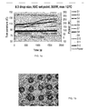
- FIG. 5 shows photographs of chip surfaces with several thermal interface materials, including a thermal interface material in accordance with aspects of the invention
- FIG. 6 shows a photograph of a control module and a module processed with Pentadecane
- FIG. 7 shows performance data of different thermal interface materials at several different sensor positions along the device
- FIG. 8 shows a first structure using the thermal interface materials in accordance with aspects of the invention.
- FIG. 9 a shows a test socket with a module attached thereto, with a heat sink in non-thermal contact with the device in accordance with aspects of the invention
- FIG. 9 b shows a test socket, where the heat sink is in thermal contact with the module using thermal interface material disposed between the module and heat sink (e.g., after actuating the heat sink into contact with the device);
- FIG. 10 shows a method of using the thermal interface materials in accordance with aspects of the invention.
- the invention relates to thermal interface materials for use with a test structure and method of use and, more particularly, to non-corrosive thermal interface materials for use in a test structure and method of use, e.g., module test and burn in.
- the thermal interface material is non-corrosive to the device under test and, more specifically, does not corrode at least the C4 (controlled collapse chip connection) structures of the device.
- the thermal interface material is electrically insulating and is capable of withstanding test conditions for a certain time and temperature during the test of the device.
- the thermal interface material can withstand conditions (e.g., not evaporate) during test from about 5 to 50 minutes at about 55° C.
- the thermal interface material of the present invention does not evaporate during test, thereby eliminating the need to at least (i) disassemble the test structure to replenish the thermal interface material, or (ii) provide an elaborate replenishment system for the test structure, both of which increase test time and costs.
- the thermal interface materials of the present invention provide improved thermal performance during test, which hence ensures that the device will not be destroyed or have its performance impaired by test procedures.
- the thermal interface material of the present invention does not leave a residue on the device, and thus does not need to be removed by solvents which, in turn, may corrode or damage the device or module. As should be understood by those of skill in the art, residue is detrimental to post test processing.
- the thermal interface material of the present invention is environmentally safe, non-toxic, and non-hazardous, and is compatible with other module (test) components (e.g., flux, underfill, capacitors, TIM, etc.) and tooling components (e.g., nozzle, syringe, piston, O-ring, connector, tubing, bottle, etc.).
- test e.g., flux, underfill, capacitors, TIM, etc.
- tooling components e.g., nozzle, syringe, piston, O-ring, connector, tubing, bottle, etc.
- the thermal interface material is an organic thermal interface material that is devoid of fluorine, chlorine, oxygen and nitrogen.
- the thermal interface material can be an organic thermal interface material that is devoid of oxygen.
- the thermal interface material is a hydrocarbon that is devoid of oxygen.
- the thermal interface material is a hydrocarbon that is devoid of fluorine, chlorine, oxygen and nitrogen.
- the thermal interface material can be a hydrocarbon that has a boiling point, in atmosphere, of between about 220° C. to about 300° C.
- the hydrocarbon is organic with 12 to 16 carbon atoms and more specifically one or more alkane with 12 to 16 carbon atoms.
- normal alkane composed of 12 to 16 carbon atoms and more specifically can be a normal alkane composed of 14 to 16 carbon atoms.
- the alkane can be Pentadecane or Hexadecane.
- FIG. 1 a shows results of a known thermal interface material mixture of water and propylene glycol tested between a 19 mm ⁇ 20 mm chip and a liquid cooled heat sink with a cooling fluid temperature of 60° C. Heat sink force was 44 lb.
- the power is off and the device is at the cooling fluid temperature, and when the power is turned on the chip heats up.
- FIG. 1 b shows corrosion residue left after testing a device with prior art water based LTI after some LTI came into contact with the chip C4s during electrical test.
- FIG. 2 shows a performance graph of an improved thermal interface material (e.g., Pentadecane) under a temperature test for 1 hour, in accordance with aspects of the invention. It should be understood that similar results (as should be understood with all of the test data herein) would also be provided with other thermal interface materials discussed herein. More specifically, FIG. 2 shows a temperature test for Pentadecane (C 15 H 32 ) as measured at several locations along a device under test. These locations are represented by “ctr” (center) and “b” through “h”, which are positions of temperature sensors along a device under test. Surprisingly, this graph shows that Pentadecane was able to withstand temperatures of about 115° C. for about an hour, without evaporating. This is shown by the steady state (e.g., constant) lines in the graphs, compared to the profile of FIG. 1 a.
- steady state e.g., constant
- the thermal interface material of the present invention can thus withstand test conditions, e.g., from about 5 to 50 minutes at about 55° C. to about 115° C., without evaporating. More specifically, it has been found that the thermal interface material of the present invention can withstand test conditions for at least 60 minutes and at least 115° C. This eliminates the need to at least (i) disassemble the test structure to replenish the thermal interface material, or (ii) provide an elaborate replenishment system for the test structure, both of which increase test time and costs.
- FIG. 3 shows a graph of data for a corrosion test (current vs. time) for various solvents, including Pentadecane (C 15 H 32 ) and Hexadecane (C 16 H 34 ) in accordance with aspects of the invention.
- This test shows Pentadecane and Hexadecane are non-corrosive materials to the C4, as well as exhibit good electrically insulating properties. It should be understood that similar results would also be provided with other thermal interface materials of the present invention, as discussed herein.
- Other materials that exhibit good thermal properties without causing corrosion include, for example, Nerol, Limonene, Pinane and Squalene; however, these materials do not exhibit, in toto, the remaining advantageous properties of the thermal interface materials of the present invention. Namely, these materials may evaporate during the test and/or leave residue on the device under test. For example, as discussed below, Nerol may leave a residue on the device under test, which would require a cleaning with solvent. It has been discovered from this experiment that all materials that had oxygen showed varying amounts of current flow and corrosion. Surprisingly, materials that did not contain oxygen did not allow current flow and had no sign of C4 corrosion.
- FIGS. 4 a and 4 b show representative devices that used thermal interface materials of the present invention during testing, in accordance with aspects of the invention. As shown in FIGS. 4 a and 4 b , devices using a test structure with Pentadecane 15 a and Hexadecane 15 b , respectively, do not exhibit any residue or corrosion of the chip C4s after testing.
- FIG. 5 shows chip surfaces at different phases of testing with different thermal interface materials, including Pentadecane in accordance with aspects of the invention.
- the testing with the interface material disposed between (in contact with) the chip and heat sink is for 30 min at 85° C. More specifically, FIG. 5 shows data for four thermal interface materials (PG (Propylene Glycol)/water (more specifically, 30% PG+70% De-ionized water), Nerol, Pentadecane and Farnesol).
- PG Polylene Glycol
- FIG. 5 shows data for four thermal interface materials (PG (Propylene Glycol)/water (more specifically, 30% PG+70% De-ionized water), Nerol, Pentadecane and Farnesol).
- PG Propylene Glycol
- the heat sink is removed and all chips except PG/Water are 100% covered by the thermal interface materials.
- the excess thermal interface materials is removed by suction in the deapplicator and then the parts were baked uncovered in an oven for 20 minutes
- Pentadecane shows many advantages over the remaining materials, one of which is no staining after the uncovered baking in an oven for 20 minutes at 70° C. This is in comparison to PG/Water, Nerol and Farnesol, each of which present issues at the same temperature.
- Nerol is a monoterpene
- Farnesol is a natural organic compound which is an acyclic sesquiterpene alcohol found as a colorless liquid.
- FIG. 5 shows that PG/water does not leave any residual, it is known to be corrosive to the C4 structure of the device under test.
- Nerol and Farnesol are non-corrosive to the C4 structure of the device under test, but they both leave residue. For example, as shown by the data of FIG. 5 , Nerol leaves a 3% stain; whereas, Farnesol leaves a 70% residue at 70° C.
- FIG. 6 shows a photograph of a control module and a module processed with Pentadecane.
- the module processed with the Pentadecane exhibited primarily aliphatic hydrocarbons at levels comparable to the control module.
- Sodium and potassium were also detected but at reduced levels relative to the control module.
- the thermal interface materials of the present invention appear to have helped clean the chip surfaces of both sodium and potassium.
- FIG. 7 shows performance data of different thermal interface materials at several different sensor positions along the device.
- helium provides non-acceptable thermal properties. It is also known that helium needs constant replenishment, as it will dissipate during test. Helium, though, is non-corrosive.
- Water e.g., PG/water
- Pentedecane provides good thermal properties, will not evaporate during test and is not corrosive to the C4 of the device under test.
- FIG. 8 shows a module using the thermal interface materials in accordance with aspects of the invention.
- the structure 10 includes a primary electronic component (device) 15 that includes interconnects (e.g., C4s) 20 for bonding to any known type of substrate 25 and/or card.
- the device 15 can be a single component (e.g., chip) or may be a combination of components (e.g., lidded module).
- the device 15 may or may not be attached on the substrate 25 and/or card that may or may not have secondary electronic components 45 with or without interconnects 30 .
- the device 15 in embodiments, is to be tested for performance, yield and/or reliability, for example.
- the substrate 25 and/or card can also include interconnects 30 a.
- the device 15 is in thermal contact with a heat sink (not shown) using a thermal interface material 40 , in order to take away (e.g., dissipate) heat from the powered device.
- the thermal interface material 40 can be in direct contact with (e.g., disposed between) the device and a heat sink.
- the thermal interface material 40 can be, for example, a normal alkane such as Pentadecane or Hexadecane.
- the normal alkane is non-corrosive, thermally stable and has good thermal performance.
- the thermal interface material 40 does not require cleaning.
- the module may also contain an underfill material surrounding the C4 interconnects (not shown) and may be covered with a lid (not shown).
- the device 15 (or chip) can have dimensions 21.3 mm ⁇ 26.7 mm with C4 interconnects powered up to at least about 340 W.
- the device or chip can have dimensions 23.6 mm ⁇ 22.0 mm with C4 interconnects powered up to at least about 400 W.
- FIG. 9 a shows the module installed in the test socket 50 after applying thermal interface material of the present invention to the surface of the chip. More specifically, FIG. 9 a shows a test socket with a module attached thereto, with a heat sink in non-thermal contact with the device. FIG. 9 b shows a test socket, where the heat sink is in thermal contact with the module using thermal interface material disposed between the module and heat sink (e.g., after actuating the heat sink into contact with the device). In this latter stage, the thermal interface material of the present invention fills the microscopic gaps between the chip and heat sink 35 thus resulting in improved temperature control.
- the socket may include a substrate clamping feature 100 and a hinged ( 35 b ) cover ( 35 a ) that incorporates a spring ( 35 c ) loaded heat sink 35 .
- the module is placed into the socket and thermal interface material placed thereon.
- the cover 35 can then be closed as shown in FIG. 9 b.
- the socket includes a primary electronic component (device) 15 that includes interconnects (e.g., C4s) 20 for bonding to any known type of substrate 25 .
- the device 15 can be attached to a ceramic substrate 25 having capacitors as secondary electronic components also attached to the substrate 25 with leaded and/or non interconnects.
- the device 15 is in thermal contact with a heat sink 35 by a thermal interface material 40 , in order to take away (e.g., dissipate) heat from the powered device.
- the thermal interface material 40 can be in direct contact with both the device 15 and the heat sink 35 .
- the heat sink 35 may be a water cooled heat-sink with a nickel plated interface to take away heat from the powered device 15 .
- the heat sink 35 may be placed in contact with the device 15 by a heat sink actuator 35 a , hinge mounted 35 b to a test board 35 d with tester electronics 55 .
- the heat sink actuator 35 a may include a spring mechanism 35 c to provide a downward pressure on the heat sink 35 .
- the heat sink 35 may include flexible supply tubing or bellows to supply cooling fluid (not shown).
- the heat sink 35 may also include heating elements and temperature sensors to actively control chip temperature. It is understood that FIG. 9 b is representative only, there are many other types of sockets, heat sinks and heat sinks actuators well known in the art. It is common that some or all parts of the process is automated.
- the thermal interface material 40 can be, for example, a normal alkane such as Pentadecane or Hexadecane. In embodiments, alkanes with 12 to 16 carbon atoms or a mixture of one or more of these alkanes or other materials discussed herein in accordance with the invention.
- the normal alkane is non corrosive, thermally stable and has good thermal performance.
- the thermal interface material 40 does not require cleaning and, after test, the device can be placed in an oven at 70° C. for 1 hour to evaporate excess thermal interface material (e.g., Pentadecane).
- FIG. 10 shows a method of implementing the present invention. More specifically, at step 1010 , a controlled weight and volume of the thermal interface material of the present invention is applied to device or heat sink.
- the weight and volume depends on the tooling attached for the test. The weight or volume for a given device/surface size is calculated or estimated on the chip size, chip and heat sink flatness, chip test temperature and test time. For example, too little weight/volume will not give complete coverage for the entire test; whereas, too much weight/volume will be a waste of material, which may spill out of the active area.
- the device is tested for a predetermined load, time and temperature.
- the load is provided to adequately make contact between the heat sink and device and thermal interface material.
- the time and temperature may be, for example, 60 minutes at 115° C. It is understood, though, that this is merely one example.
- the test device/module and heat sink/socket are separated.
- the device is heated to evaporate the thermal interface material of the present invention.
- Table 1 shows examples of weights, loads, wattage, test time and test temperature.
- the methods as described above is used in the fabrication of integrated circuit chips.
- the resulting integrated circuit chips can be distributed by the fabricator as a bare die, or in a packaged form. In the latter case the chip is mounted in a single chip package (such as a plastic carrier, with leads that are affixed to a motherboard or other higher level carrier) or in a multichip package (such as a ceramic carrier that has either or both surface interconnections or buried interconnections). In any case the chip is then integrated with other chips, discrete circuit elements, and/or other signal processing devices as part of either (a) an intermediate product, such as a motherboard, or (b) an end product.
- the end product can be any product that includes integrated circuit chips.
Landscapes
- Engineering & Computer Science (AREA)
- Computer Hardware Design (AREA)
- Microelectronics & Electronic Packaging (AREA)
- General Engineering & Computer Science (AREA)
- Physics & Mathematics (AREA)
- General Physics & Mathematics (AREA)
- Testing Of Individual Semiconductor Devices (AREA)
- Testing Resistance To Weather, Investigating Materials By Mechanical Methods (AREA)
Abstract
Description
| TABLE 1 | ||||||
| Chip | LTI | Test | Test | |||
| Chip Size | Power | Weight | Load | Time | Temp | |
| Example | mm × mm | Watt | mg | lbf | min | ° C. |
| 1 | 14.7 × 14.7 | 320 | 2.1 | 12.5 | 60 | 115 |
| 2 | 20.9 × 21.7 | 75-350 | 4.0 | 3.5 | 15 | 85 |
Claims (24)
Priority Applications (1)
| Application Number | Priority Date | Filing Date | Title |
|---|---|---|---|
| US12/770,948 US8686749B2 (en) | 2010-04-30 | 2010-04-30 | Thermal interface material, test structure and method of use |
Applications Claiming Priority (1)
| Application Number | Priority Date | Filing Date | Title |
|---|---|---|---|
| US12/770,948 US8686749B2 (en) | 2010-04-30 | 2010-04-30 | Thermal interface material, test structure and method of use |
Publications (2)
| Publication Number | Publication Date |
|---|---|
| US20110267084A1 US20110267084A1 (en) | 2011-11-03 |
| US8686749B2 true US8686749B2 (en) | 2014-04-01 |
Family
ID=44857756
Family Applications (1)
| Application Number | Title | Priority Date | Filing Date |
|---|---|---|---|
| US12/770,948 Active 2032-07-02 US8686749B2 (en) | 2010-04-30 | 2010-04-30 | Thermal interface material, test structure and method of use |
Country Status (1)
| Country | Link |
|---|---|
| US (1) | US8686749B2 (en) |
Cited By (1)
| Publication number | Priority date | Publication date | Assignee | Title |
|---|---|---|---|---|
| US20160081231A1 (en) * | 2014-09-11 | 2016-03-17 | Dell Products L.P. | Information Handling System Heat Sink Compatibility Management |
Families Citing this family (3)
| Publication number | Priority date | Publication date | Assignee | Title |
|---|---|---|---|---|
| US9244107B2 (en) * | 2012-11-12 | 2016-01-26 | Marvell World Trade Ltd. | Heat sink blade pack for device under test testing |
| US9269603B2 (en) * | 2013-05-09 | 2016-02-23 | Globalfoundries Inc. | Temporary liquid thermal interface material for surface tension adhesion and thermal control |
| US10401423B2 (en) * | 2016-05-03 | 2019-09-03 | Teradyne, Inc. | Thermal control using phase-change material |
Citations (15)
| Publication number | Priority date | Publication date | Assignee | Title |
|---|---|---|---|---|
| US5088006A (en) | 1991-04-25 | 1992-02-11 | International Business Machines Corporation | Liquid film interface cooling system for semiconductor wafer processing |
| US5224356A (en) * | 1991-09-30 | 1993-07-06 | Triangle Research & Development Corp. | Method of using thermal energy absorbing and conducting potting materials |
| US5918665A (en) | 1997-04-04 | 1999-07-06 | Unisys Corporation | Method of thermal coupling an electronic device to a heat exchange member while said electronic device is being tested |
| US6797382B2 (en) * | 1999-12-01 | 2004-09-28 | Honeywell International Inc. | Thermal interface materials |
| US20040191501A1 (en) * | 2001-10-18 | 2004-09-30 | Rasiah Ignatius J | Electrically conductive thermal interface |
| US20060090881A1 (en) | 2004-10-29 | 2006-05-04 | 3M Innovative Properties Company | Immersion cooling apparatus |
| US7141448B2 (en) * | 1999-03-03 | 2006-11-28 | Intel Corporation | Controlled collapse chip connection (C4) integrated circuit package which has two dissimilar underfill materials |
| US20070051773A1 (en) * | 2005-09-02 | 2007-03-08 | Ruchert Brian D | Thermal interface materials, methods of preparation thereof and their applications |
| US20070161521A1 (en) | 2006-01-12 | 2007-07-12 | Sachdev Krishna G | Enhanced thermo-oxidative stability thermal interface compositions and use thereof in microelectronics assembly |
| US7259580B2 (en) | 2005-02-22 | 2007-08-21 | International Business Machines Corporation | Method and apparatus for temporary thermal coupling of an electronic device to a heat sink during test |
| US20070290378A1 (en) * | 2006-06-20 | 2007-12-20 | International Business Machines Corporation | Novel reworkable underfills for ceramic mcm c4 protection |
| US20080298016A1 (en) | 2005-06-14 | 2008-12-04 | International Business Machines Corporation | Cooling an electronic device utilizing spring elements with fins |
| US20090281254A1 (en) | 2008-05-06 | 2009-11-12 | International Business Machines Corporation | Liquid thermal interface having mixture of linearly structured polymer doped crosslinked networks and related method |
| US20100006255A1 (en) | 2007-01-17 | 2010-01-14 | Bilodeau Stephane | Energy recuperation system |
| US7651340B2 (en) * | 2007-02-23 | 2010-01-26 | Essai, Inc. | Chip actuator cover assembly |
-
2010
- 2010-04-30 US US12/770,948 patent/US8686749B2/en active Active
Patent Citations (15)
| Publication number | Priority date | Publication date | Assignee | Title |
|---|---|---|---|---|
| US5088006A (en) | 1991-04-25 | 1992-02-11 | International Business Machines Corporation | Liquid film interface cooling system for semiconductor wafer processing |
| US5224356A (en) * | 1991-09-30 | 1993-07-06 | Triangle Research & Development Corp. | Method of using thermal energy absorbing and conducting potting materials |
| US5918665A (en) | 1997-04-04 | 1999-07-06 | Unisys Corporation | Method of thermal coupling an electronic device to a heat exchange member while said electronic device is being tested |
| US7141448B2 (en) * | 1999-03-03 | 2006-11-28 | Intel Corporation | Controlled collapse chip connection (C4) integrated circuit package which has two dissimilar underfill materials |
| US6797382B2 (en) * | 1999-12-01 | 2004-09-28 | Honeywell International Inc. | Thermal interface materials |
| US20040191501A1 (en) * | 2001-10-18 | 2004-09-30 | Rasiah Ignatius J | Electrically conductive thermal interface |
| US20060090881A1 (en) | 2004-10-29 | 2006-05-04 | 3M Innovative Properties Company | Immersion cooling apparatus |
| US7259580B2 (en) | 2005-02-22 | 2007-08-21 | International Business Machines Corporation | Method and apparatus for temporary thermal coupling of an electronic device to a heat sink during test |
| US20080298016A1 (en) | 2005-06-14 | 2008-12-04 | International Business Machines Corporation | Cooling an electronic device utilizing spring elements with fins |
| US20070051773A1 (en) * | 2005-09-02 | 2007-03-08 | Ruchert Brian D | Thermal interface materials, methods of preparation thereof and their applications |
| US20070161521A1 (en) | 2006-01-12 | 2007-07-12 | Sachdev Krishna G | Enhanced thermo-oxidative stability thermal interface compositions and use thereof in microelectronics assembly |
| US20070290378A1 (en) * | 2006-06-20 | 2007-12-20 | International Business Machines Corporation | Novel reworkable underfills for ceramic mcm c4 protection |
| US20100006255A1 (en) | 2007-01-17 | 2010-01-14 | Bilodeau Stephane | Energy recuperation system |
| US7651340B2 (en) * | 2007-02-23 | 2010-01-26 | Essai, Inc. | Chip actuator cover assembly |
| US20090281254A1 (en) | 2008-05-06 | 2009-11-12 | International Business Machines Corporation | Liquid thermal interface having mixture of linearly structured polymer doped crosslinked networks and related method |
Non-Patent Citations (8)
| Title |
|---|
| A.A. Mills et al., "Rate of evaporation of hydrocarbons from a hot surface: Nukiyama and Leidenfrost temperatures," Eur. J. Phys. vol. 3., 1982, pp. 152-154. |
| ChemSpider, the free cheical database, ID 11885, Pentadecane, p. 1-3. * |
| DeHaven, Keith, et al., Controlled collapse chip connection (C4)-an enabling technology, Proc. 44th Elec. Compon. & Tech. Conf., 1994, May 1-4, 1994, p. 1. * |
| DeHaven, Keith, et al., Controlled collapse chip connection (C4)—an enabling technology, Proc. 44th Elec. Compon. & Tech. Conf., 1994, May 1-4, 1994, p. 1. * |
| Epoxies 50-1225 Technical Bulletin, Thermally Conductive Silicone Rubber, Jun. 2003, p. 1-2. * |
| Si,gma, Product Information, Hexadecane Product No. H0255, Apr. 2003, p. 1. * |
| Stiver, Warren, Evaporation times and rates of specific hydrocarbons in oil spills, Environ. Sci. and Tech., 1989, 23, 101-105. * |
| Waldstein, Analysis of pump oil and alkanes evaporation, U of S. Floriday, Masters Thesis, 2008, p. 1-89. * |
Cited By (2)
| Publication number | Priority date | Publication date | Assignee | Title |
|---|---|---|---|---|
| US20160081231A1 (en) * | 2014-09-11 | 2016-03-17 | Dell Products L.P. | Information Handling System Heat Sink Compatibility Management |
| US9915984B2 (en) * | 2014-09-11 | 2018-03-13 | Dell Products L.P. | Information handling system heat sink compatibility management |
Also Published As
| Publication number | Publication date |
|---|---|
| US20110267084A1 (en) | 2011-11-03 |
Similar Documents
| Publication | Publication Date | Title |
|---|---|---|
| US8471575B2 (en) | Methodologies and test configurations for testing thermal interface materials | |
| US11692271B2 (en) | Immersion cooling with water-based fluid using nano-structured coating | |
| Swamy et al. | A review of the performance and characterization of conventional and promising thermal interface materials for electronic package applications | |
| Di Cioccio et al. | An overview of patterned metal/dielectric surface bonding: Mechanism, alignment and characterization | |
| JP5731405B2 (en) | Low compressive force non-silicone high thermal conductivity formulations and packages for thermal interface materials | |
| US7332927B2 (en) | Apparatus for temporary thermal coupling of an electronic device to a heat sink during test | |
| US5297621A (en) | Method and apparatus for maintaining electrically operating device temperatures | |
| US8686749B2 (en) | Thermal interface material, test structure and method of use | |
| JP6343571B2 (en) | Package on Package Thermal Force Device | |
| US20160315030A1 (en) | Reusable thermoplastic thermal interface materials and methods for establishing thermal joints between heat sources and heat dissipating/removal structures | |
| US7285971B2 (en) | Integrated circuit (IC) test assembly including phase change material for stabilizing temperature during stress testing of integrated circuits and method thereof | |
| Hanß et al. | Transient thermal analysis as measurement method for IC package structural integrity | |
| US8535956B2 (en) | Chip attach frame | |
| JPS6211509B2 (en) | ||
| US20170219303A1 (en) | Flexible metallic heat connector | |
| US20090009204A1 (en) | Test socket | |
| Gao et al. | Development of low temperature direct bond interconnect technology for die-to-wafer and die-to-die applications-stacking, yield improvement, reliability assessment | |
| US20090152713A1 (en) | Integrated circuit assembly including thermal interface material comprised of oil or wax | |
| El-Genk | Combined effects of subcooling and surface orientation on pool boiling of HFE-7100 from a simulated electronic chip | |
| Fruehauf et al. | Chip-package-board reliability of System-in-Package using laminate chip embedding technology based on Cu leadframe | |
| TW200509338A (en) | Heat dissipation apparatus for package device | |
| AboRas et al. | Development and fabrication of a thin film thermo test chip and its integration into a test system for thermal interface characterization | |
| Raypah et al. | Effects of solder paste on thermal and optical performance of high-power ThinGaN white LED | |
| Gong et al. | On-chip hotspot thermal delay and peak clipping using a heterogeneously integrated micro-thermoelectric cooler | |
| Ramakrishnan | Viability of server module thermal management using enhanced heat sinks and low global warming potential dielectric fluids |
Legal Events
| Date | Code | Title | Description |
|---|---|---|---|
| AS | Assignment |
Owner name: INTERNATIONAL BUSINESS MACHINES CORPORATION, NEW Y Free format text: ASSIGNMENT OF ASSIGNORS INTEREST;ASSIGNORS:ERWIN, BRIAN M.;GARDELL, DAVID L.;HUMENIK, JAMES N.;AND OTHERS;SIGNING DATES FROM 20100423 TO 20100426;REEL/FRAME:024316/0318 |
|
| STCF | Information on status: patent grant |
Free format text: PATENTED CASE |
|
| AS | Assignment |
Owner name: GLOBALFOUNDRIES U.S. 2 LLC, NEW YORK Free format text: ASSIGNMENT OF ASSIGNORS INTEREST;ASSIGNOR:INTERNATIONAL BUSINESS MACHINES CORPORATION;REEL/FRAME:036550/0001 Effective date: 20150629 |
|
| AS | Assignment |
Owner name: GLOBALFOUNDRIES INC., CAYMAN ISLANDS Free format text: ASSIGNMENT OF ASSIGNORS INTEREST;ASSIGNORS:GLOBALFOUNDRIES U.S. 2 LLC;GLOBALFOUNDRIES U.S. INC.;REEL/FRAME:036779/0001 Effective date: 20150910 |
|
| MAFP | Maintenance fee payment |
Free format text: PAYMENT OF MAINTENANCE FEE, 4TH YEAR, LARGE ENTITY (ORIGINAL EVENT CODE: M1551) Year of fee payment: 4 |
|
| AS | Assignment |
Owner name: WILMINGTON TRUST, NATIONAL ASSOCIATION, DELAWARE Free format text: SECURITY AGREEMENT;ASSIGNOR:GLOBALFOUNDRIES INC.;REEL/FRAME:049490/0001 Effective date: 20181127 |
|
| AS | Assignment |
Owner name: GLOBALFOUNDRIES U.S. INC., CALIFORNIA Free format text: ASSIGNMENT OF ASSIGNORS INTEREST;ASSIGNOR:GLOBALFOUNDRIES INC.;REEL/FRAME:054633/0001 Effective date: 20201022 |
|
| AS | Assignment |
Owner name: GLOBALFOUNDRIES INC., CAYMAN ISLANDS Free format text: RELEASE BY SECURED PARTY;ASSIGNOR:WILMINGTON TRUST, NATIONAL ASSOCIATION;REEL/FRAME:054636/0001 Effective date: 20201117 |
|
| AS | Assignment |
Owner name: GLOBALFOUNDRIES U.S. INC., NEW YORK Free format text: RELEASE BY SECURED PARTY;ASSIGNOR:WILMINGTON TRUST, NATIONAL ASSOCIATION;REEL/FRAME:056987/0001 Effective date: 20201117 |
|
| MAFP | Maintenance fee payment |
Free format text: PAYMENT OF MAINTENANCE FEE, 8TH YEAR, LARGE ENTITY (ORIGINAL EVENT CODE: M1552); ENTITY STATUS OF PATENT OWNER: LARGE ENTITY Year of fee payment: 8 |