US8673688B2 - Semiconductor package and method of manufacturing the same - Google Patents

Semiconductor package and method of manufacturing the same Download PDF

Info

Publication number
US8673688B2
US8673688B2 US13/227,889 US201113227889A US8673688B2 US 8673688 B2 US8673688 B2 US 8673688B2 US 201113227889 A US201113227889 A US 201113227889A US 8673688 B2 US8673688 B2 US 8673688B2
Authority
US
United States
Prior art keywords
substrate
dummy
metal pattern
forming
connection terminal
Prior art date
Legal status (The legal status is an assumption and is not a legal conclusion. Google has not performed a legal analysis and makes no representation as to the accuracy of the status listed.)
Active, expires
Application number
US13/227,889
Other versions
US20120100671A1 (en
Inventor
Wonkeun Kim
Current Assignee (The listed assignees may be inaccurate. Google has not performed a legal analysis and makes no representation or warranty as to the accuracy of the list.)
Samsung Electronics Co Ltd
Original Assignee
Samsung Electronics Co Ltd
Priority date (The priority date is an assumption and is not a legal conclusion. Google has not performed a legal analysis and makes no representation as to the accuracy of the date listed.)
Filing date
Publication date
Application filed by Samsung Electronics Co Ltd filed Critical Samsung Electronics Co Ltd
Assigned to SAMSUNG ELECTRONICS CO., LTD. reassignment SAMSUNG ELECTRONICS CO., LTD. ASSIGNMENT OF ASSIGNORS INTEREST (SEE DOCUMENT FOR DETAILS). Assignors: KIM, WONKEUN
Publication of US20120100671A1 publication Critical patent/US20120100671A1/en
Application granted granted Critical
Publication of US8673688B2 publication Critical patent/US8673688B2/en
Active legal-status Critical Current
Adjusted expiration legal-status Critical

Links

Images

Classifications

    • HELECTRICITY
    • H01ELECTRIC ELEMENTS
    • H01LSEMICONDUCTOR DEVICES NOT COVERED BY CLASS H10
    • H01L21/00Processes or apparatus adapted for the manufacture or treatment of semiconductor or solid state devices or of parts thereof
    • H01L21/02Manufacture or treatment of semiconductor devices or of parts thereof
    • H01L21/04Manufacture or treatment of semiconductor devices or of parts thereof the devices having at least one potential-jump barrier or surface barrier, e.g. PN junction, depletion layer or carrier concentration layer
    • H01L21/50Assembly of semiconductor devices using processes or apparatus not provided for in a single one of the subgroups H01L21/06 - H01L21/326, e.g. sealing of a cap to a base of a container
    • H01L21/56Encapsulations, e.g. encapsulation layers, coatings
    • H01L21/563Encapsulation of active face of flip-chip device, e.g. underfilling or underencapsulation of flip-chip, encapsulation preform on chip or mounting substrate
    • HELECTRICITY
    • H01ELECTRIC ELEMENTS
    • H01LSEMICONDUCTOR DEVICES NOT COVERED BY CLASS H10
    • H01L23/00Details of semiconductor or other solid state devices
    • H01L23/28Encapsulations, e.g. encapsulating layers, coatings, e.g. for protection
    • H01L23/31Encapsulations, e.g. encapsulating layers, coatings, e.g. for protection characterised by the arrangement or shape
    • H01L23/3107Encapsulations, e.g. encapsulating layers, coatings, e.g. for protection characterised by the arrangement or shape the device being completely enclosed
    • H01L23/3121Encapsulations, e.g. encapsulating layers, coatings, e.g. for protection characterised by the arrangement or shape the device being completely enclosed a substrate forming part of the encapsulation
    • H01L23/3128Encapsulations, e.g. encapsulating layers, coatings, e.g. for protection characterised by the arrangement or shape the device being completely enclosed a substrate forming part of the encapsulation the substrate having spherical bumps for external connection
    • HELECTRICITY
    • H01ELECTRIC ELEMENTS
    • H01LSEMICONDUCTOR DEVICES NOT COVERED BY CLASS H10
    • H01L23/00Details of semiconductor or other solid state devices
    • H01L23/48Arrangements for conducting electric current to or from the solid state body in operation, e.g. leads, terminal arrangements ; Selection of materials therefor
    • H01L23/488Arrangements for conducting electric current to or from the solid state body in operation, e.g. leads, terminal arrangements ; Selection of materials therefor consisting of soldered or bonded constructions
    • H01L23/498Leads, i.e. metallisations or lead-frames on insulating substrates, e.g. chip carriers
    • H01L23/49811Additional leads joined to the metallisation on the insulating substrate, e.g. pins, bumps, wires, flat leads
    • HELECTRICITY
    • H01ELECTRIC ELEMENTS
    • H01LSEMICONDUCTOR DEVICES NOT COVERED BY CLASS H10
    • H01L23/00Details of semiconductor or other solid state devices
    • H01L23/48Arrangements for conducting electric current to or from the solid state body in operation, e.g. leads, terminal arrangements ; Selection of materials therefor
    • H01L23/488Arrangements for conducting electric current to or from the solid state body in operation, e.g. leads, terminal arrangements ; Selection of materials therefor consisting of soldered or bonded constructions
    • H01L23/498Leads, i.e. metallisations or lead-frames on insulating substrates, e.g. chip carriers
    • H01L23/49827Via connections through the substrates, e.g. pins going through the substrate, coaxial cables
    • HELECTRICITY
    • H01ELECTRIC ELEMENTS
    • H01LSEMICONDUCTOR DEVICES NOT COVERED BY CLASS H10
    • H01L23/00Details of semiconductor or other solid state devices
    • H01L23/58Structural electrical arrangements for semiconductor devices not otherwise provided for, e.g. in combination with batteries
    • H01L23/585Structural electrical arrangements for semiconductor devices not otherwise provided for, e.g. in combination with batteries comprising conductive layers or plates or strips or rods or rings
    • HELECTRICITY
    • H01ELECTRIC ELEMENTS
    • H01LSEMICONDUCTOR DEVICES NOT COVERED BY CLASS H10
    • H01L24/00Arrangements for connecting or disconnecting semiconductor or solid-state bodies; Methods or apparatus related thereto
    • H01L24/01Means for bonding being attached to, or being formed on, the surface to be connected, e.g. chip-to-package, die-attach, "first-level" interconnects; Manufacturing methods related thereto
    • H01L24/10Bump connectors ; Manufacturing methods related thereto
    • H01L24/15Structure, shape, material or disposition of the bump connectors after the connecting process
    • H01L24/16Structure, shape, material or disposition of the bump connectors after the connecting process of an individual bump connector
    • HELECTRICITY
    • H01ELECTRIC ELEMENTS
    • H01LSEMICONDUCTOR DEVICES NOT COVERED BY CLASS H10
    • H01L24/00Arrangements for connecting or disconnecting semiconductor or solid-state bodies; Methods or apparatus related thereto
    • H01L24/01Means for bonding being attached to, or being formed on, the surface to be connected, e.g. chip-to-package, die-attach, "first-level" interconnects; Manufacturing methods related thereto
    • H01L24/26Layer connectors, e.g. plate connectors, solder or adhesive layers; Manufacturing methods related thereto
    • H01L24/28Structure, shape, material or disposition of the layer connectors prior to the connecting process
    • H01L24/29Structure, shape, material or disposition of the layer connectors prior to the connecting process of an individual layer connector
    • HELECTRICITY
    • H01ELECTRIC ELEMENTS
    • H01LSEMICONDUCTOR DEVICES NOT COVERED BY CLASS H10
    • H01L24/00Arrangements for connecting or disconnecting semiconductor or solid-state bodies; Methods or apparatus related thereto
    • H01L24/73Means for bonding being of different types provided for in two or more of groups H01L24/10, H01L24/18, H01L24/26, H01L24/34, H01L24/42, H01L24/50, H01L24/63, H01L24/71
    • HELECTRICITY
    • H01ELECTRIC ELEMENTS
    • H01LSEMICONDUCTOR DEVICES NOT COVERED BY CLASS H10
    • H01L24/00Arrangements for connecting or disconnecting semiconductor or solid-state bodies; Methods or apparatus related thereto
    • H01L24/80Methods for connecting semiconductor or other solid state bodies using means for bonding being attached to, or being formed on, the surface to be connected
    • H01L24/83Methods for connecting semiconductor or other solid state bodies using means for bonding being attached to, or being formed on, the surface to be connected using a layer connector
    • HELECTRICITY
    • H01ELECTRIC ELEMENTS
    • H01LSEMICONDUCTOR DEVICES NOT COVERED BY CLASS H10
    • H01L25/00Assemblies consisting of a plurality of individual semiconductor or other solid state devices ; Multistep manufacturing processes thereof
    • H01L25/03Assemblies consisting of a plurality of individual semiconductor or other solid state devices ; Multistep manufacturing processes thereof all the devices being of a type provided for in the same subgroup of groups H01L27/00 - H01L33/00, or in a single subclass of H10K, H10N, e.g. assemblies of rectifier diodes
    • H01L25/04Assemblies consisting of a plurality of individual semiconductor or other solid state devices ; Multistep manufacturing processes thereof all the devices being of a type provided for in the same subgroup of groups H01L27/00 - H01L33/00, or in a single subclass of H10K, H10N, e.g. assemblies of rectifier diodes the devices not having separate containers
    • H01L25/065Assemblies consisting of a plurality of individual semiconductor or other solid state devices ; Multistep manufacturing processes thereof all the devices being of a type provided for in the same subgroup of groups H01L27/00 - H01L33/00, or in a single subclass of H10K, H10N, e.g. assemblies of rectifier diodes the devices not having separate containers the devices being of a type provided for in group H01L27/00
    • H01L25/0657Stacked arrangements of devices
    • HELECTRICITY
    • H01ELECTRIC ELEMENTS
    • H01LSEMICONDUCTOR DEVICES NOT COVERED BY CLASS H10
    • H01L2224/00Indexing scheme for arrangements for connecting or disconnecting semiconductor or solid-state bodies and methods related thereto as covered by H01L24/00
    • H01L2224/01Means for bonding being attached to, or being formed on, the surface to be connected, e.g. chip-to-package, die-attach, "first-level" interconnects; Manufacturing methods related thereto
    • H01L2224/10Bump connectors; Manufacturing methods related thereto
    • H01L2224/15Structure, shape, material or disposition of the bump connectors after the connecting process
    • H01L2224/16Structure, shape, material or disposition of the bump connectors after the connecting process of an individual bump connector
    • H01L2224/161Disposition
    • H01L2224/16135Disposition the bump connector connecting between different semiconductor or solid-state bodies, i.e. chip-to-chip
    • H01L2224/16145Disposition the bump connector connecting between different semiconductor or solid-state bodies, i.e. chip-to-chip the bodies being stacked
    • HELECTRICITY
    • H01ELECTRIC ELEMENTS
    • H01LSEMICONDUCTOR DEVICES NOT COVERED BY CLASS H10
    • H01L2224/00Indexing scheme for arrangements for connecting or disconnecting semiconductor or solid-state bodies and methods related thereto as covered by H01L24/00
    • H01L2224/01Means for bonding being attached to, or being formed on, the surface to be connected, e.g. chip-to-package, die-attach, "first-level" interconnects; Manufacturing methods related thereto
    • H01L2224/10Bump connectors; Manufacturing methods related thereto
    • H01L2224/15Structure, shape, material or disposition of the bump connectors after the connecting process
    • H01L2224/16Structure, shape, material or disposition of the bump connectors after the connecting process of an individual bump connector
    • H01L2224/161Disposition
    • H01L2224/16151Disposition the bump connector connecting between a semiconductor or solid-state body and an item not being a semiconductor or solid-state body, e.g. chip-to-substrate, chip-to-passive
    • H01L2224/16221Disposition the bump connector connecting between a semiconductor or solid-state body and an item not being a semiconductor or solid-state body, e.g. chip-to-substrate, chip-to-passive the body and the item being stacked
    • H01L2224/16225Disposition the bump connector connecting between a semiconductor or solid-state body and an item not being a semiconductor or solid-state body, e.g. chip-to-substrate, chip-to-passive the body and the item being stacked the item being non-metallic, e.g. insulating substrate with or without metallisation
    • HELECTRICITY
    • H01ELECTRIC ELEMENTS
    • H01LSEMICONDUCTOR DEVICES NOT COVERED BY CLASS H10
    • H01L2224/00Indexing scheme for arrangements for connecting or disconnecting semiconductor or solid-state bodies and methods related thereto as covered by H01L24/00
    • H01L2224/01Means for bonding being attached to, or being formed on, the surface to be connected, e.g. chip-to-package, die-attach, "first-level" interconnects; Manufacturing methods related thereto
    • H01L2224/26Layer connectors, e.g. plate connectors, solder or adhesive layers; Manufacturing methods related thereto
    • H01L2224/2612Auxiliary members for layer connectors, e.g. spacers
    • H01L2224/26122Auxiliary members for layer connectors, e.g. spacers being formed on the semiconductor or solid-state body to be connected
    • HELECTRICITY
    • H01ELECTRIC ELEMENTS
    • H01LSEMICONDUCTOR DEVICES NOT COVERED BY CLASS H10
    • H01L2224/00Indexing scheme for arrangements for connecting or disconnecting semiconductor or solid-state bodies and methods related thereto as covered by H01L24/00
    • H01L2224/01Means for bonding being attached to, or being formed on, the surface to be connected, e.g. chip-to-package, die-attach, "first-level" interconnects; Manufacturing methods related thereto
    • H01L2224/26Layer connectors, e.g. plate connectors, solder or adhesive layers; Manufacturing methods related thereto
    • H01L2224/2612Auxiliary members for layer connectors, e.g. spacers
    • H01L2224/26152Auxiliary members for layer connectors, e.g. spacers being formed on an item to be connected not being a semiconductor or solid-state body
    • HELECTRICITY
    • H01ELECTRIC ELEMENTS
    • H01LSEMICONDUCTOR DEVICES NOT COVERED BY CLASS H10
    • H01L2224/00Indexing scheme for arrangements for connecting or disconnecting semiconductor or solid-state bodies and methods related thereto as covered by H01L24/00
    • H01L2224/01Means for bonding being attached to, or being formed on, the surface to be connected, e.g. chip-to-package, die-attach, "first-level" interconnects; Manufacturing methods related thereto
    • H01L2224/26Layer connectors, e.g. plate connectors, solder or adhesive layers; Manufacturing methods related thereto
    • H01L2224/28Structure, shape, material or disposition of the layer connectors prior to the connecting process
    • H01L2224/29Structure, shape, material or disposition of the layer connectors prior to the connecting process of an individual layer connector
    • H01L2224/29001Core members of the layer connector
    • H01L2224/29075Plural core members
    • H01L2224/2908Plural core members being stacked
    • H01L2224/29083Three-layer arrangements
    • HELECTRICITY
    • H01ELECTRIC ELEMENTS
    • H01LSEMICONDUCTOR DEVICES NOT COVERED BY CLASS H10
    • H01L2224/00Indexing scheme for arrangements for connecting or disconnecting semiconductor or solid-state bodies and methods related thereto as covered by H01L24/00
    • H01L2224/01Means for bonding being attached to, or being formed on, the surface to be connected, e.g. chip-to-package, die-attach, "first-level" interconnects; Manufacturing methods related thereto
    • H01L2224/26Layer connectors, e.g. plate connectors, solder or adhesive layers; Manufacturing methods related thereto
    • H01L2224/28Structure, shape, material or disposition of the layer connectors prior to the connecting process
    • H01L2224/29Structure, shape, material or disposition of the layer connectors prior to the connecting process of an individual layer connector
    • H01L2224/29001Core members of the layer connector
    • H01L2224/29099Material
    • H01L2224/291Material with a principal constituent of the material being a metal or a metalloid, e.g. boron [B], silicon [Si], germanium [Ge], arsenic [As], antimony [Sb], tellurium [Te] and polonium [Po], and alloys thereof
    • H01L2224/29101Material with a principal constituent of the material being a metal or a metalloid, e.g. boron [B], silicon [Si], germanium [Ge], arsenic [As], antimony [Sb], tellurium [Te] and polonium [Po], and alloys thereof the principal constituent melting at a temperature of less than 400°C
    • HELECTRICITY
    • H01ELECTRIC ELEMENTS
    • H01LSEMICONDUCTOR DEVICES NOT COVERED BY CLASS H10
    • H01L2224/00Indexing scheme for arrangements for connecting or disconnecting semiconductor or solid-state bodies and methods related thereto as covered by H01L24/00
    • H01L2224/01Means for bonding being attached to, or being formed on, the surface to be connected, e.g. chip-to-package, die-attach, "first-level" interconnects; Manufacturing methods related thereto
    • H01L2224/26Layer connectors, e.g. plate connectors, solder or adhesive layers; Manufacturing methods related thereto
    • H01L2224/28Structure, shape, material or disposition of the layer connectors prior to the connecting process
    • H01L2224/29Structure, shape, material or disposition of the layer connectors prior to the connecting process of an individual layer connector
    • H01L2224/29001Core members of the layer connector
    • H01L2224/29099Material
    • H01L2224/2919Material with a principal constituent of the material being a polymer, e.g. polyester, phenolic based polymer, epoxy
    • HELECTRICITY
    • H01ELECTRIC ELEMENTS
    • H01LSEMICONDUCTOR DEVICES NOT COVERED BY CLASS H10
    • H01L2224/00Indexing scheme for arrangements for connecting or disconnecting semiconductor or solid-state bodies and methods related thereto as covered by H01L24/00
    • H01L2224/01Means for bonding being attached to, or being formed on, the surface to be connected, e.g. chip-to-package, die-attach, "first-level" interconnects; Manufacturing methods related thereto
    • H01L2224/26Layer connectors, e.g. plate connectors, solder or adhesive layers; Manufacturing methods related thereto
    • H01L2224/28Structure, shape, material or disposition of the layer connectors prior to the connecting process
    • H01L2224/29Structure, shape, material or disposition of the layer connectors prior to the connecting process of an individual layer connector
    • H01L2224/29001Core members of the layer connector
    • H01L2224/29099Material
    • H01L2224/29198Material with a principal constituent of the material being a combination of two or more materials in the form of a matrix with a filler, i.e. being a hybrid material, e.g. segmented structures, foams
    • H01L2224/29199Material of the matrix
    • H01L2224/2929Material of the matrix with a principal constituent of the material being a polymer, e.g. polyester, phenolic based polymer, epoxy
    • HELECTRICITY
    • H01ELECTRIC ELEMENTS
    • H01LSEMICONDUCTOR DEVICES NOT COVERED BY CLASS H10
    • H01L2224/00Indexing scheme for arrangements for connecting or disconnecting semiconductor or solid-state bodies and methods related thereto as covered by H01L24/00
    • H01L2224/01Means for bonding being attached to, or being formed on, the surface to be connected, e.g. chip-to-package, die-attach, "first-level" interconnects; Manufacturing methods related thereto
    • H01L2224/26Layer connectors, e.g. plate connectors, solder or adhesive layers; Manufacturing methods related thereto
    • H01L2224/28Structure, shape, material or disposition of the layer connectors prior to the connecting process
    • H01L2224/29Structure, shape, material or disposition of the layer connectors prior to the connecting process of an individual layer connector
    • H01L2224/29001Core members of the layer connector
    • H01L2224/29099Material
    • H01L2224/29198Material with a principal constituent of the material being a combination of two or more materials in the form of a matrix with a filler, i.e. being a hybrid material, e.g. segmented structures, foams
    • H01L2224/29298Fillers
    • H01L2224/29299Base material
    • H01L2224/293Base material with a principal constituent of the material being a metal or a metalloid, e.g. boron [B], silicon [Si], germanium [Ge], arsenic [As], antimony [Sb], tellurium [Te] and polonium [Po], and alloys thereof
    • H01L2224/29301Base material with a principal constituent of the material being a metal or a metalloid, e.g. boron [B], silicon [Si], germanium [Ge], arsenic [As], antimony [Sb], tellurium [Te] and polonium [Po], and alloys thereof the principal constituent melting at a temperature of less than 400°C
    • H01L2224/29309Indium [In] as principal constituent
    • HELECTRICITY
    • H01ELECTRIC ELEMENTS
    • H01LSEMICONDUCTOR DEVICES NOT COVERED BY CLASS H10
    • H01L2224/00Indexing scheme for arrangements for connecting or disconnecting semiconductor or solid-state bodies and methods related thereto as covered by H01L24/00
    • H01L2224/01Means for bonding being attached to, or being formed on, the surface to be connected, e.g. chip-to-package, die-attach, "first-level" interconnects; Manufacturing methods related thereto
    • H01L2224/26Layer connectors, e.g. plate connectors, solder or adhesive layers; Manufacturing methods related thereto
    • H01L2224/28Structure, shape, material or disposition of the layer connectors prior to the connecting process
    • H01L2224/29Structure, shape, material or disposition of the layer connectors prior to the connecting process of an individual layer connector
    • H01L2224/29001Core members of the layer connector
    • H01L2224/29099Material
    • H01L2224/29198Material with a principal constituent of the material being a combination of two or more materials in the form of a matrix with a filler, i.e. being a hybrid material, e.g. segmented structures, foams
    • H01L2224/29298Fillers
    • H01L2224/29299Base material
    • H01L2224/293Base material with a principal constituent of the material being a metal or a metalloid, e.g. boron [B], silicon [Si], germanium [Ge], arsenic [As], antimony [Sb], tellurium [Te] and polonium [Po], and alloys thereof
    • H01L2224/29301Base material with a principal constituent of the material being a metal or a metalloid, e.g. boron [B], silicon [Si], germanium [Ge], arsenic [As], antimony [Sb], tellurium [Te] and polonium [Po], and alloys thereof the principal constituent melting at a temperature of less than 400°C
    • H01L2224/29311Tin [Sn] as principal constituent
    • HELECTRICITY
    • H01ELECTRIC ELEMENTS
    • H01LSEMICONDUCTOR DEVICES NOT COVERED BY CLASS H10
    • H01L2224/00Indexing scheme for arrangements for connecting or disconnecting semiconductor or solid-state bodies and methods related thereto as covered by H01L24/00
    • H01L2224/01Means for bonding being attached to, or being formed on, the surface to be connected, e.g. chip-to-package, die-attach, "first-level" interconnects; Manufacturing methods related thereto
    • H01L2224/26Layer connectors, e.g. plate connectors, solder or adhesive layers; Manufacturing methods related thereto
    • H01L2224/28Structure, shape, material or disposition of the layer connectors prior to the connecting process
    • H01L2224/29Structure, shape, material or disposition of the layer connectors prior to the connecting process of an individual layer connector
    • H01L2224/29001Core members of the layer connector
    • H01L2224/29099Material
    • H01L2224/29198Material with a principal constituent of the material being a combination of two or more materials in the form of a matrix with a filler, i.e. being a hybrid material, e.g. segmented structures, foams
    • H01L2224/29298Fillers
    • H01L2224/29299Base material
    • H01L2224/293Base material with a principal constituent of the material being a metal or a metalloid, e.g. boron [B], silicon [Si], germanium [Ge], arsenic [As], antimony [Sb], tellurium [Te] and polonium [Po], and alloys thereof
    • H01L2224/29301Base material with a principal constituent of the material being a metal or a metalloid, e.g. boron [B], silicon [Si], germanium [Ge], arsenic [As], antimony [Sb], tellurium [Te] and polonium [Po], and alloys thereof the principal constituent melting at a temperature of less than 400°C
    • H01L2224/29313Bismuth [Bi] as principal constituent
    • HELECTRICITY
    • H01ELECTRIC ELEMENTS
    • H01LSEMICONDUCTOR DEVICES NOT COVERED BY CLASS H10
    • H01L2224/00Indexing scheme for arrangements for connecting or disconnecting semiconductor or solid-state bodies and methods related thereto as covered by H01L24/00
    • H01L2224/01Means for bonding being attached to, or being formed on, the surface to be connected, e.g. chip-to-package, die-attach, "first-level" interconnects; Manufacturing methods related thereto
    • H01L2224/26Layer connectors, e.g. plate connectors, solder or adhesive layers; Manufacturing methods related thereto
    • H01L2224/28Structure, shape, material or disposition of the layer connectors prior to the connecting process
    • H01L2224/29Structure, shape, material or disposition of the layer connectors prior to the connecting process of an individual layer connector
    • H01L2224/29001Core members of the layer connector
    • H01L2224/29099Material
    • H01L2224/29198Material with a principal constituent of the material being a combination of two or more materials in the form of a matrix with a filler, i.e. being a hybrid material, e.g. segmented structures, foams
    • H01L2224/29298Fillers
    • H01L2224/29299Base material
    • H01L2224/293Base material with a principal constituent of the material being a metal or a metalloid, e.g. boron [B], silicon [Si], germanium [Ge], arsenic [As], antimony [Sb], tellurium [Te] and polonium [Po], and alloys thereof
    • H01L2224/29301Base material with a principal constituent of the material being a metal or a metalloid, e.g. boron [B], silicon [Si], germanium [Ge], arsenic [As], antimony [Sb], tellurium [Te] and polonium [Po], and alloys thereof the principal constituent melting at a temperature of less than 400°C
    • H01L2224/29316Lead [Pb] as principal constituent
    • HELECTRICITY
    • H01ELECTRIC ELEMENTS
    • H01LSEMICONDUCTOR DEVICES NOT COVERED BY CLASS H10
    • H01L2224/00Indexing scheme for arrangements for connecting or disconnecting semiconductor or solid-state bodies and methods related thereto as covered by H01L24/00
    • H01L2224/01Means for bonding being attached to, or being formed on, the surface to be connected, e.g. chip-to-package, die-attach, "first-level" interconnects; Manufacturing methods related thereto
    • H01L2224/26Layer connectors, e.g. plate connectors, solder or adhesive layers; Manufacturing methods related thereto
    • H01L2224/28Structure, shape, material or disposition of the layer connectors prior to the connecting process
    • H01L2224/29Structure, shape, material or disposition of the layer connectors prior to the connecting process of an individual layer connector
    • H01L2224/29001Core members of the layer connector
    • H01L2224/29099Material
    • H01L2224/29198Material with a principal constituent of the material being a combination of two or more materials in the form of a matrix with a filler, i.e. being a hybrid material, e.g. segmented structures, foams
    • H01L2224/29298Fillers
    • H01L2224/29299Base material
    • H01L2224/293Base material with a principal constituent of the material being a metal or a metalloid, e.g. boron [B], silicon [Si], germanium [Ge], arsenic [As], antimony [Sb], tellurium [Te] and polonium [Po], and alloys thereof
    • H01L2224/29317Base material with a principal constituent of the material being a metal or a metalloid, e.g. boron [B], silicon [Si], germanium [Ge], arsenic [As], antimony [Sb], tellurium [Te] and polonium [Po], and alloys thereof the principal constituent melting at a temperature of greater than or equal to 400°C and less than 950°C
    • H01L2224/2932Antimony [Sb] as principal constituent
    • HELECTRICITY
    • H01ELECTRIC ELEMENTS
    • H01LSEMICONDUCTOR DEVICES NOT COVERED BY CLASS H10
    • H01L2224/00Indexing scheme for arrangements for connecting or disconnecting semiconductor or solid-state bodies and methods related thereto as covered by H01L24/00
    • H01L2224/01Means for bonding being attached to, or being formed on, the surface to be connected, e.g. chip-to-package, die-attach, "first-level" interconnects; Manufacturing methods related thereto
    • H01L2224/26Layer connectors, e.g. plate connectors, solder or adhesive layers; Manufacturing methods related thereto
    • H01L2224/28Structure, shape, material or disposition of the layer connectors prior to the connecting process
    • H01L2224/29Structure, shape, material or disposition of the layer connectors prior to the connecting process of an individual layer connector
    • H01L2224/29001Core members of the layer connector
    • H01L2224/29099Material
    • H01L2224/29198Material with a principal constituent of the material being a combination of two or more materials in the form of a matrix with a filler, i.e. being a hybrid material, e.g. segmented structures, foams
    • H01L2224/29298Fillers
    • H01L2224/29299Base material
    • H01L2224/293Base material with a principal constituent of the material being a metal or a metalloid, e.g. boron [B], silicon [Si], germanium [Ge], arsenic [As], antimony [Sb], tellurium [Te] and polonium [Po], and alloys thereof
    • H01L2224/29338Base material with a principal constituent of the material being a metal or a metalloid, e.g. boron [B], silicon [Si], germanium [Ge], arsenic [As], antimony [Sb], tellurium [Te] and polonium [Po], and alloys thereof the principal constituent melting at a temperature of greater than or equal to 950°C and less than 1550°C
    • H01L2224/29339Silver [Ag] as principal constituent
    • HELECTRICITY
    • H01ELECTRIC ELEMENTS
    • H01LSEMICONDUCTOR DEVICES NOT COVERED BY CLASS H10
    • H01L2224/00Indexing scheme for arrangements for connecting or disconnecting semiconductor or solid-state bodies and methods related thereto as covered by H01L24/00
    • H01L2224/01Means for bonding being attached to, or being formed on, the surface to be connected, e.g. chip-to-package, die-attach, "first-level" interconnects; Manufacturing methods related thereto
    • H01L2224/26Layer connectors, e.g. plate connectors, solder or adhesive layers; Manufacturing methods related thereto
    • H01L2224/28Structure, shape, material or disposition of the layer connectors prior to the connecting process
    • H01L2224/29Structure, shape, material or disposition of the layer connectors prior to the connecting process of an individual layer connector
    • H01L2224/29001Core members of the layer connector
    • H01L2224/29099Material
    • H01L2224/29198Material with a principal constituent of the material being a combination of two or more materials in the form of a matrix with a filler, i.e. being a hybrid material, e.g. segmented structures, foams
    • H01L2224/29298Fillers
    • H01L2224/29299Base material
    • H01L2224/293Base material with a principal constituent of the material being a metal or a metalloid, e.g. boron [B], silicon [Si], germanium [Ge], arsenic [As], antimony [Sb], tellurium [Te] and polonium [Po], and alloys thereof
    • H01L2224/29338Base material with a principal constituent of the material being a metal or a metalloid, e.g. boron [B], silicon [Si], germanium [Ge], arsenic [As], antimony [Sb], tellurium [Te] and polonium [Po], and alloys thereof the principal constituent melting at a temperature of greater than or equal to 950°C and less than 1550°C
    • H01L2224/29347Copper [Cu] as principal constituent
    • HELECTRICITY
    • H01ELECTRIC ELEMENTS
    • H01LSEMICONDUCTOR DEVICES NOT COVERED BY CLASS H10
    • H01L2224/00Indexing scheme for arrangements for connecting or disconnecting semiconductor or solid-state bodies and methods related thereto as covered by H01L24/00
    • H01L2224/01Means for bonding being attached to, or being formed on, the surface to be connected, e.g. chip-to-package, die-attach, "first-level" interconnects; Manufacturing methods related thereto
    • H01L2224/26Layer connectors, e.g. plate connectors, solder or adhesive layers; Manufacturing methods related thereto
    • H01L2224/31Structure, shape, material or disposition of the layer connectors after the connecting process
    • H01L2224/32Structure, shape, material or disposition of the layer connectors after the connecting process of an individual layer connector
    • H01L2224/321Disposition
    • H01L2224/32151Disposition the layer connector connecting between a semiconductor or solid-state body and an item not being a semiconductor or solid-state body, e.g. chip-to-substrate, chip-to-passive
    • H01L2224/32221Disposition the layer connector connecting between a semiconductor or solid-state body and an item not being a semiconductor or solid-state body, e.g. chip-to-substrate, chip-to-passive the body and the item being stacked
    • H01L2224/32225Disposition the layer connector connecting between a semiconductor or solid-state body and an item not being a semiconductor or solid-state body, e.g. chip-to-substrate, chip-to-passive the body and the item being stacked the item being non-metallic, e.g. insulating substrate with or without metallisation
    • HELECTRICITY
    • H01ELECTRIC ELEMENTS
    • H01LSEMICONDUCTOR DEVICES NOT COVERED BY CLASS H10
    • H01L2224/00Indexing scheme for arrangements for connecting or disconnecting semiconductor or solid-state bodies and methods related thereto as covered by H01L24/00
    • H01L2224/73Means for bonding being of different types provided for in two or more of groups H01L2224/10, H01L2224/18, H01L2224/26, H01L2224/34, H01L2224/42, H01L2224/50, H01L2224/63, H01L2224/71
    • H01L2224/732Location after the connecting process
    • H01L2224/73201Location after the connecting process on the same surface
    • H01L2224/73203Bump and layer connectors
    • H01L2224/73204Bump and layer connectors the bump connector being embedded into the layer connector
    • HELECTRICITY
    • H01ELECTRIC ELEMENTS
    • H01LSEMICONDUCTOR DEVICES NOT COVERED BY CLASS H10
    • H01L2224/00Indexing scheme for arrangements for connecting or disconnecting semiconductor or solid-state bodies and methods related thereto as covered by H01L24/00
    • H01L2224/80Methods for connecting semiconductor or other solid state bodies using means for bonding being attached to, or being formed on, the surface to be connected
    • H01L2224/83Methods for connecting semiconductor or other solid state bodies using means for bonding being attached to, or being formed on, the surface to be connected using a layer connector
    • H01L2224/8319Arrangement of the layer connectors prior to mounting
    • H01L2224/83192Arrangement of the layer connectors prior to mounting wherein the layer connectors are disposed only on another item or body to be connected to the semiconductor or solid-state body
    • HELECTRICITY
    • H01ELECTRIC ELEMENTS
    • H01LSEMICONDUCTOR DEVICES NOT COVERED BY CLASS H10
    • H01L2224/00Indexing scheme for arrangements for connecting or disconnecting semiconductor or solid-state bodies and methods related thereto as covered by H01L24/00
    • H01L2224/80Methods for connecting semiconductor or other solid state bodies using means for bonding being attached to, or being formed on, the surface to be connected
    • H01L2224/83Methods for connecting semiconductor or other solid state bodies using means for bonding being attached to, or being formed on, the surface to be connected using a layer connector
    • H01L2224/838Bonding techniques
    • H01L2224/8385Bonding techniques using a polymer adhesive, e.g. an adhesive based on silicone, epoxy, polyimide, polyester
    • H01L2224/83851Bonding techniques using a polymer adhesive, e.g. an adhesive based on silicone, epoxy, polyimide, polyester being an anisotropic conductive adhesive
    • HELECTRICITY
    • H01ELECTRIC ELEMENTS
    • H01LSEMICONDUCTOR DEVICES NOT COVERED BY CLASS H10
    • H01L2224/00Indexing scheme for arrangements for connecting or disconnecting semiconductor or solid-state bodies and methods related thereto as covered by H01L24/00
    • H01L2224/80Methods for connecting semiconductor or other solid state bodies using means for bonding being attached to, or being formed on, the surface to be connected
    • H01L2224/83Methods for connecting semiconductor or other solid state bodies using means for bonding being attached to, or being formed on, the surface to be connected using a layer connector
    • H01L2224/838Bonding techniques
    • H01L2224/8385Bonding techniques using a polymer adhesive, e.g. an adhesive based on silicone, epoxy, polyimide, polyester
    • H01L2224/83855Hardening the adhesive by curing, i.e. thermosetting
    • H01L2224/83862Heat curing
    • HELECTRICITY
    • H01ELECTRIC ELEMENTS
    • H01LSEMICONDUCTOR DEVICES NOT COVERED BY CLASS H10
    • H01L2224/00Indexing scheme for arrangements for connecting or disconnecting semiconductor or solid-state bodies and methods related thereto as covered by H01L24/00
    • H01L2224/80Methods for connecting semiconductor or other solid state bodies using means for bonding being attached to, or being formed on, the surface to be connected
    • H01L2224/83Methods for connecting semiconductor or other solid state bodies using means for bonding being attached to, or being formed on, the surface to be connected using a layer connector
    • H01L2224/838Bonding techniques
    • H01L2224/83886Involving a self-assembly process, e.g. self-agglomeration of a material dispersed in a fluid
    • H01L2224/83888Involving a self-assembly process, e.g. self-agglomeration of a material dispersed in a fluid with special adaptation of the surface of the body to be connected, e.g. surface shape specially adapted for the self-assembly process
    • HELECTRICITY
    • H01ELECTRIC ELEMENTS
    • H01LSEMICONDUCTOR DEVICES NOT COVERED BY CLASS H10
    • H01L2224/00Indexing scheme for arrangements for connecting or disconnecting semiconductor or solid-state bodies and methods related thereto as covered by H01L24/00
    • H01L2224/80Methods for connecting semiconductor or other solid state bodies using means for bonding being attached to, or being formed on, the surface to be connected
    • H01L2224/83Methods for connecting semiconductor or other solid state bodies using means for bonding being attached to, or being formed on, the surface to be connected using a layer connector
    • H01L2224/83986Specific sequence of steps, e.g. repetition of manufacturing steps, time sequence
    • HELECTRICITY
    • H01ELECTRIC ELEMENTS
    • H01LSEMICONDUCTOR DEVICES NOT COVERED BY CLASS H10
    • H01L2225/00Details relating to assemblies covered by the group H01L25/00 but not provided for in its subgroups
    • H01L2225/03All the devices being of a type provided for in the same subgroup of groups H01L27/00 - H01L33/648 and H10K99/00
    • H01L2225/04All the devices being of a type provided for in the same subgroup of groups H01L27/00 - H01L33/648 and H10K99/00 the devices not having separate containers
    • H01L2225/065All the devices being of a type provided for in the same subgroup of groups H01L27/00 - H01L33/648 and H10K99/00 the devices not having separate containers the devices being of a type provided for in group H01L27/00
    • H01L2225/06503Stacked arrangements of devices
    • H01L2225/06513Bump or bump-like direct electrical connections between devices, e.g. flip-chip connection, solder bumps
    • HELECTRICITY
    • H01ELECTRIC ELEMENTS
    • H01LSEMICONDUCTOR DEVICES NOT COVERED BY CLASS H10
    • H01L2225/00Details relating to assemblies covered by the group H01L25/00 but not provided for in its subgroups
    • H01L2225/03All the devices being of a type provided for in the same subgroup of groups H01L27/00 - H01L33/648 and H10K99/00
    • H01L2225/04All the devices being of a type provided for in the same subgroup of groups H01L27/00 - H01L33/648 and H10K99/00 the devices not having separate containers
    • H01L2225/065All the devices being of a type provided for in the same subgroup of groups H01L27/00 - H01L33/648 and H10K99/00 the devices not having separate containers the devices being of a type provided for in group H01L27/00
    • H01L2225/06503Stacked arrangements of devices
    • H01L2225/06517Bump or bump-like direct electrical connections from device to substrate
    • HELECTRICITY
    • H01ELECTRIC ELEMENTS
    • H01LSEMICONDUCTOR DEVICES NOT COVERED BY CLASS H10
    • H01L2225/00Details relating to assemblies covered by the group H01L25/00 but not provided for in its subgroups
    • H01L2225/03All the devices being of a type provided for in the same subgroup of groups H01L27/00 - H01L33/648 and H10K99/00
    • H01L2225/04All the devices being of a type provided for in the same subgroup of groups H01L27/00 - H01L33/648 and H10K99/00 the devices not having separate containers
    • H01L2225/065All the devices being of a type provided for in the same subgroup of groups H01L27/00 - H01L33/648 and H10K99/00 the devices not having separate containers the devices being of a type provided for in group H01L27/00
    • H01L2225/06503Stacked arrangements of devices
    • H01L2225/06541Conductive via connections through the device, e.g. vertical interconnects, through silicon via [TSV]
    • HELECTRICITY
    • H01ELECTRIC ELEMENTS
    • H01LSEMICONDUCTOR DEVICES NOT COVERED BY CLASS H10
    • H01L23/00Details of semiconductor or other solid state devices
    • H01L23/12Mountings, e.g. non-detachable insulating substrates
    • H01L23/13Mountings, e.g. non-detachable insulating substrates characterised by the shape
    • HELECTRICITY
    • H01ELECTRIC ELEMENTS
    • H01LSEMICONDUCTOR DEVICES NOT COVERED BY CLASS H10
    • H01L23/00Details of semiconductor or other solid state devices
    • H01L23/48Arrangements for conducting electric current to or from the solid state body in operation, e.g. leads, terminal arrangements ; Selection of materials therefor
    • H01L23/488Arrangements for conducting electric current to or from the solid state body in operation, e.g. leads, terminal arrangements ; Selection of materials therefor consisting of soldered or bonded constructions
    • H01L23/498Leads, i.e. metallisations or lead-frames on insulating substrates, e.g. chip carriers
    • H01L23/49811Additional leads joined to the metallisation on the insulating substrate, e.g. pins, bumps, wires, flat leads
    • H01L23/49816Spherical bumps on the substrate for external connection, e.g. ball grid arrays [BGA]
    • HELECTRICITY
    • H01ELECTRIC ELEMENTS
    • H01LSEMICONDUCTOR DEVICES NOT COVERED BY CLASS H10
    • H01L23/00Details of semiconductor or other solid state devices
    • H01L23/48Arrangements for conducting electric current to or from the solid state body in operation, e.g. leads, terminal arrangements ; Selection of materials therefor
    • H01L23/488Arrangements for conducting electric current to or from the solid state body in operation, e.g. leads, terminal arrangements ; Selection of materials therefor consisting of soldered or bonded constructions
    • H01L23/498Leads, i.e. metallisations or lead-frames on insulating substrates, e.g. chip carriers
    • H01L23/49838Geometry or layout
    • HELECTRICITY
    • H01ELECTRIC ELEMENTS
    • H01LSEMICONDUCTOR DEVICES NOT COVERED BY CLASS H10
    • H01L24/00Arrangements for connecting or disconnecting semiconductor or solid-state bodies; Methods or apparatus related thereto
    • H01L24/01Means for bonding being attached to, or being formed on, the surface to be connected, e.g. chip-to-package, die-attach, "first-level" interconnects; Manufacturing methods related thereto
    • H01L24/26Layer connectors, e.g. plate connectors, solder or adhesive layers; Manufacturing methods related thereto
    • H01L24/31Structure, shape, material or disposition of the layer connectors after the connecting process
    • H01L24/32Structure, shape, material or disposition of the layer connectors after the connecting process of an individual layer connector
    • HELECTRICITY
    • H01ELECTRIC ELEMENTS
    • H01LSEMICONDUCTOR DEVICES NOT COVERED BY CLASS H10
    • H01L2924/00Indexing scheme for arrangements or methods for connecting or disconnecting semiconductor or solid-state bodies as covered by H01L24/00
    • H01L2924/01Chemical elements
    • H01L2924/01005Boron [B]
    • HELECTRICITY
    • H01ELECTRIC ELEMENTS
    • H01LSEMICONDUCTOR DEVICES NOT COVERED BY CLASS H10
    • H01L2924/00Indexing scheme for arrangements or methods for connecting or disconnecting semiconductor or solid-state bodies as covered by H01L24/00
    • H01L2924/01Chemical elements
    • H01L2924/01006Carbon [C]
    • HELECTRICITY
    • H01ELECTRIC ELEMENTS
    • H01LSEMICONDUCTOR DEVICES NOT COVERED BY CLASS H10
    • H01L2924/00Indexing scheme for arrangements or methods for connecting or disconnecting semiconductor or solid-state bodies as covered by H01L24/00
    • H01L2924/01Chemical elements
    • H01L2924/01029Copper [Cu]
    • HELECTRICITY
    • H01ELECTRIC ELEMENTS
    • H01LSEMICONDUCTOR DEVICES NOT COVERED BY CLASS H10
    • H01L2924/00Indexing scheme for arrangements or methods for connecting or disconnecting semiconductor or solid-state bodies as covered by H01L24/00
    • H01L2924/01Chemical elements
    • H01L2924/01033Arsenic [As]
    • HELECTRICITY
    • H01ELECTRIC ELEMENTS
    • H01LSEMICONDUCTOR DEVICES NOT COVERED BY CLASS H10
    • H01L2924/00Indexing scheme for arrangements or methods for connecting or disconnecting semiconductor or solid-state bodies as covered by H01L24/00
    • H01L2924/01Chemical elements
    • H01L2924/01047Silver [Ag]
    • HELECTRICITY
    • H01ELECTRIC ELEMENTS
    • H01LSEMICONDUCTOR DEVICES NOT COVERED BY CLASS H10
    • H01L2924/00Indexing scheme for arrangements or methods for connecting or disconnecting semiconductor or solid-state bodies as covered by H01L24/00
    • H01L2924/01Chemical elements
    • H01L2924/01049Indium [In]
    • HELECTRICITY
    • H01ELECTRIC ELEMENTS
    • H01LSEMICONDUCTOR DEVICES NOT COVERED BY CLASS H10
    • H01L2924/00Indexing scheme for arrangements or methods for connecting or disconnecting semiconductor or solid-state bodies as covered by H01L24/00
    • H01L2924/01Chemical elements
    • H01L2924/0105Tin [Sn]
    • HELECTRICITY
    • H01ELECTRIC ELEMENTS
    • H01LSEMICONDUCTOR DEVICES NOT COVERED BY CLASS H10
    • H01L2924/00Indexing scheme for arrangements or methods for connecting or disconnecting semiconductor or solid-state bodies as covered by H01L24/00
    • H01L2924/01Chemical elements
    • H01L2924/01051Antimony [Sb]
    • HELECTRICITY
    • H01ELECTRIC ELEMENTS
    • H01LSEMICONDUCTOR DEVICES NOT COVERED BY CLASS H10
    • H01L2924/00Indexing scheme for arrangements or methods for connecting or disconnecting semiconductor or solid-state bodies as covered by H01L24/00
    • H01L2924/01Chemical elements
    • H01L2924/01074Tungsten [W]
    • HELECTRICITY
    • H01ELECTRIC ELEMENTS
    • H01LSEMICONDUCTOR DEVICES NOT COVERED BY CLASS H10
    • H01L2924/00Indexing scheme for arrangements or methods for connecting or disconnecting semiconductor or solid-state bodies as covered by H01L24/00
    • H01L2924/01Chemical elements
    • H01L2924/01082Lead [Pb]
    • HELECTRICITY
    • H01ELECTRIC ELEMENTS
    • H01LSEMICONDUCTOR DEVICES NOT COVERED BY CLASS H10
    • H01L2924/00Indexing scheme for arrangements or methods for connecting or disconnecting semiconductor or solid-state bodies as covered by H01L24/00
    • H01L2924/013Alloys
    • H01L2924/014Solder alloys
    • HELECTRICITY
    • H01ELECTRIC ELEMENTS
    • H01LSEMICONDUCTOR DEVICES NOT COVERED BY CLASS H10
    • H01L2924/00Indexing scheme for arrangements or methods for connecting or disconnecting semiconductor or solid-state bodies as covered by H01L24/00
    • H01L2924/06Polymers
    • H01L2924/0665Epoxy resin
    • HELECTRICITY
    • H01ELECTRIC ELEMENTS
    • H01LSEMICONDUCTOR DEVICES NOT COVERED BY CLASS H10
    • H01L2924/00Indexing scheme for arrangements or methods for connecting or disconnecting semiconductor or solid-state bodies as covered by H01L24/00
    • H01L2924/095Indexing scheme for arrangements or methods for connecting or disconnecting semiconductor or solid-state bodies as covered by H01L24/00 with a principal constituent of the material being a combination of two or more materials provided in the groups H01L2924/013 - H01L2924/0715
    • H01L2924/097Glass-ceramics, e.g. devitrified glass
    • H01L2924/09701Low temperature co-fired ceramic [LTCC]
    • HELECTRICITY
    • H01ELECTRIC ELEMENTS
    • H01LSEMICONDUCTOR DEVICES NOT COVERED BY CLASS H10
    • H01L2924/00Indexing scheme for arrangements or methods for connecting or disconnecting semiconductor or solid-state bodies as covered by H01L24/00
    • H01L2924/10Details of semiconductor or other solid state devices to be connected
    • H01L2924/11Device type
    • H01L2924/14Integrated circuits
    • HELECTRICITY
    • H01ELECTRIC ELEMENTS
    • H01LSEMICONDUCTOR DEVICES NOT COVERED BY CLASS H10
    • H01L2924/00Indexing scheme for arrangements or methods for connecting or disconnecting semiconductor or solid-state bodies as covered by H01L24/00
    • H01L2924/15Details of package parts other than the semiconductor or other solid state devices to be connected
    • H01L2924/151Die mounting substrate
    • H01L2924/153Connection portion
    • H01L2924/1531Connection portion the connection portion being formed only on the surface of the substrate opposite to the die mounting surface
    • H01L2924/15311Connection portion the connection portion being formed only on the surface of the substrate opposite to the die mounting surface being a ball array, e.g. BGA

Definitions

  • the present disclosure herein relates to a semiconductor package and a method of manufacturing the same.
  • flip chip bonding mounting is extensively used for reducing wiring delay as a semiconductor chip is mounted on a circuit substrate (or a wiring substrate). More reliable and simpler flip chip bonding mounting methods are diversely studied in relation to a manufacturing method of a semiconductor package.
  • the present disclosure provides a reliable semiconductor package.
  • the present disclosure also provides a reliable manufacturing method of a semiconductor package.
  • One example embodiment includes a circuit substrate including a base substrate.
  • a substrate connection terminal is on the base substrate, and a substrate insulation layer on the base substrate exposes the substrate connection terminal.
  • the package further includes a first semiconductor chip, which includes a chip connection terminal and a chip insulation layer.
  • the chip insulation layer exposes the chip connection terminal and is mounted on the circuit substrate.
  • An inner solder ball is between the substrate connection terminal and the chip connection terminal. The inner solder ball electrically connects the substrate connection terminal to the chip connection terminal.
  • a dummy solder fills a dummy opening in at least one of the substrate insulation layer and the chip insulation layer. The dummy solder does not electrically connect the semiconductor chip with the substrate.
  • the circuit substrate may further include a via metal pattern on an inner sidewall of a via hole that penetrates.
  • a dummy opening is in the substrate insulation layer and exposes the via metal pattern, and the dummy solder contacts the via metal pattern and at least partially fills the via hole.
  • the circuit substrate may further include a circuit metal pattern electrically connected to the substrate connection terminal.
  • the substrate insulation layer includes the dummy opening, which exposes the circuit metal pattern.
  • a width of the dummy opening greater than a width of the circuit metal pattern.
  • the circuit substrate may further include a substrate dummy metal pattern.
  • the substrate insulation layer includes the dummy opening, which may expose the substrate dummy metal pattern.
  • the dummy solder may contact the dummy metal pattern.
  • a width of the dummy opening may be greater than a width of the substrate dummy metal pattern.
  • the circuit substrate may further include a recess metal pattern on a sidewall and a bottom of a recessed region of the circuit substrate.
  • the substrate insulation layer includes the dummy opening, which exposes the recess metal pattern.
  • the dummy solder contacts the recess metal pattern and at least partially fills the recessed region.
  • the semiconductor chip may further include a chip dummy metal pattern, and a dummy opening is in the chip insulation layer.
  • the dummy opening exposes the chip dummy metal pattern, and the dummy solder contacts the chip dummy metal pattern.
  • the first semiconductor chip may further include a bump on the chip connection terminal, and the inner solder ball may cover at least a side of the bump.
  • the semiconductor chip may further include a through via penetrating the first semiconductor chip.
  • the semiconductor package may further include a second semiconductor chip mounted on the first semiconductor chip and connected electrically to the through via.
  • One embodiment of the method includes forming a circuit substrate including a base substrate.
  • a substrate connection terminal is on the base substrate, and a substrate insulation layer covers the base substrate and exposes the substrate connection terminal.
  • a mixture layer is formed on the circuit substrate and includes an adhesive resin and a solder particle.
  • a first semiconductor chip is provided on the mixture layer.
  • the first semiconductor chip includes a chip connection terminal and a chip insulation layer, which exposes the chip connection terminal.
  • the method further includes forming an inner solder ball between the substrate connection terminal and the chip connection terminal, and forming dummy solder in a dummy opening. The dummy opening is in one of the substrate insulation layer and the chip insulation layer.
  • the solder particles are dispersed in the adhesive resin.
  • the forming the mixture layer may include providing a mixed multilayer including an adhesive resin layer formed of the adhesive resin and a solder particle layer formed of the solder particles.
  • the forming of the inner solder ball may include heating with the mixture layer to a temperature of more than a melting point of the solder particles.
  • the forming of the circuit substrate may include preparing the base substrate; forming the substrate connection terminal on the base substrate; and forming the substrate insulation layer on the base substrate such that the substrate insulation layer exposes the substrate connection terminal.
  • the methods may further include forming a circuit metal pattern on the base substrate.
  • the substrate insulation layer includes a dummy opening exposing the circuit metal pattern.
  • the dummy opening has a width greater than a width of the circuit metal pattern.
  • the methods may further include forming a via hole by patterning the base substrate, and forming a via metal pattern on a sidewall of the via hole, wherein the substrate insulation layer includes a dummy opening exposing the via metal pattern.
  • the methods may further include forming a recessed region in the base substrate, and forming a recess metal pattern covering a sidewall and a bottom of the recessed region, wherein the substrate insulation layer is formed to have a dummy opening exposing the recess metal pattern.
  • the methods may further include forming a substrate dummy metal pattern on the base substrate, wherein the substrate insulation layer is formed to have a dummy opening exposing the substrate dummy metal pattern.
  • the dummy opening has a width greater than a width of the substrate dummy metal pattern.
  • the methods may further include forming an upper mixture layer on the first semiconductor chip; and providing a second semiconductor chip on the upper mixture layer.
  • the second semiconductor chip includes an upper chip connection terminal and an upper chip insulation layer exposing the upper chip connection terminal.
  • An upper inner solder ball is formed between the chip connection terminal and the upper chip connection terminal.
  • the forming of the inner solder ball and the forming of the upper inner solder ball may be performed simultaneously.
  • the method includes forming at least one dummy opening in at least one of an insulation layer of a semiconductor chip and an insulation layer of a substrate.
  • An inner solder ball is formed between the substrate and the semiconductor chip. The inner solder ball electrically connects a chip connecting terminal of the semiconductor chip to a substrate connection terminal of the substrate.
  • a dummy solder is formed in the at least one dummy opening, and the dummy solder does not electrically connect the substrate to the semiconductor chip.
  • the method further includes forming at least one of a circuit metal pattern, a via metal pattern, and a dummy substrate metal pattern on the substrate; wherein the at least one dummy opening is formed to expose at least one of the circuit metal pattern, the via metal pattern, and the dummy substrate metal pattern.
  • the method further includes forming a circuit metal pattern, a via metal pattern, and a dummy substrate metal pattern on the substrate; wherein the at least one dummy opening is a plurality of dummy openings formed to expose the circuit metal pattern, the via metal pattern, and the dummy substrate metal pattern.
  • the method further includes forming a mixture layer on the substrate.
  • the mixture layer includes an adhesive resin and a plurality of solder particles, and the inner solder ball and the dummy solder are simultaneously formed by heating the mixture layer.
  • the solder particles may be dispersed in the adhesive resin.
  • the forming the mixture layer includes providing a mixed multilayer having an adhesive resin layer formed of the adhesive resin and a solder particle layer formed of the solder particles.
  • FIG. 1 is a plan view of a semiconductor package according to a first example embodiment of the inventive concepts
  • FIG. 2 is a sectional view taken along the line II-II′ of FIG. 1 .
  • FIGS. 3 through 8 , 9 A, 10 A, and 12 are manufacturing sectional views illustrating sequential manufacturing processes of a semiconductor package having a section of FIG. 2 according to an example embodiment of the inventive concepts;
  • FIG. 9B is an enlarged perspective view of a portion A of FIG. 9A ;
  • FIG. 10B is an enlarged sectional view of a portion B of FIG. 10A ;
  • FIG. 11A is a manufacturing sectional view illustrating a semiconductor package having a section of FIG. 2 according to another example embodiment of the inventive concepts
  • FIG. 11B is an enlarged sectional view of a portion C of FIG. 11A ;
  • FIG. 13 is a plan view of a semiconductor package according to a second example embodiment of the inventive concepts.
  • FIG. 14A is a sectional view taken along the line XIVA-XIVA′ of FIG. 13 ;
  • FIG. 14B is a sectional view taken along the line XIVB-XIVB′ of FIG. 13 .
  • FIGS. 15A through 19A are manufacturing sectional views illustrating sequential manufacturing processes of a semiconductor package having a section of FIG. 14A ;
  • FIGS. 15B through 19B are manufacturing sectional views illustrating sequential manufacturing processes of a semiconductor package having a section of FIG. 14B ;
  • FIG. 18C is an enlarged perspective view of a portion D of FIG. 18A ;
  • FIG. 20 is a sectional view of a semiconductor package according to a third example embodiment.
  • FIG. 21 is a sectional view of a semiconductor package according to a fourth example embodiment of the inventive concepts.
  • FIG. 22 is a sectional view of a semiconductor package according to a fifth example embodiment.
  • FIGS. 23 through 26 are manufacturing sectional views illustrating sequential manufacturing processes of a semiconductor package having a section of FIG. 22 according to an example embodiment of the inventive concepts
  • FIG. 27 is a manufacturing sectional view illustrating sequential manufacturing processes of a semiconductor package having a section of FIG. 22 according to another example embodiment of the inventive concepts;
  • FIG. 28 is a view illustrating an example of a package module including a semiconductor package that the technique of the inventive concepts is applied;
  • FIG. 29 is a block diagram illustrating an example of an electronic device including a semiconductor package that the technique of the inventive concepts is applied.
  • FIG. 30 is a block diagram illustrating a memory system with a semiconductor package that the technique of the inventive concepts is applied.
  • Example embodiments will be described more fully hereinafter with reference to the accompanying drawings, in which example embodiments are shown.
  • the present invention may, however, be embodied in many different forms and should not be construed as limited to example embodiments as set forth herein. Rather, example embodiments are provided so that this disclosure will be thorough and complete, and will fully convey the scope of the present invention to those skilled in the art.
  • the sizes and relative sizes of layers and regions may be exaggerated for clarity.
  • first, second, third etc. may be used herein to describe various elements, components, regions, layers and/or sections, these elements, components, regions, layers and/or sections should not be limited by these terms. These terms are only used to distinguish one element, component, region, layer or section from another region, layer or section. Thus, a first element, component, region, layer or section discussed below could be termed a second element, component, region, layer or section without departing from the teachings of the present invention.
  • spatially relative terms such as “beneath,” “below,” “lower,” “above,” “upper” and the like, may be used herein for ease of description to describe one element or feature's relationship to another element(s) or feature(s) as illustrated in the figures. It will be understood that the spatially relative terms are intended to encompass different orientations of the device in use or operation in addition to the orientation depicted in the figures. For example, if the device in the figures is turned over, elements described as “below” or “beneath” other elements or features would then be oriented “above” the other elements or features. Thus, the exemplary term “below” can encompass both an orientation of above and below. The device may be otherwise oriented (rotated 90 degrees or at other orientations) and the spatially relative descriptors used herein interpreted accordingly.
  • Example embodiments are described herein with reference to cross-sectional illustrations that are schematic illustrations of idealized example embodiments (and intermediate structures). As such, variations from the shapes of the illustrations as a result, for example, of manufacturing techniques and/or tolerances, are to be expected. Thus, example embodiments should not be construed as limited to the particular shapes of regions illustrated herein but are to include deviations in shapes that result, for example, from manufacturing. For example, an implanted region illustrated as a rectangle will, typically, have rounded or curved features and/or a gradient of implant concentration at its edges rather than a binary change from implanted to non-implanted region.
  • a buried region formed by implantation may result in some implantation in the region between the buried region and the surface through which the implantation takes place.
  • the regions illustrated in the figures are schematic in nature and their shapes are not intended to illustrate the actual shape of a region of a device and are not intended to limit the scope of the present invention.
  • FIG. 1 is a plan view of a semiconductor package according to a first example embodiment (embodiment 1) of the inventive concepts.
  • FIG. 2 is a sectional view taken along the line II-II′ of FIG. 1 .
  • the semiconductor package 300 of the embodiment 1 includes a circuit substrate 100 and a semiconductor chip 200 mounted thereon.
  • the circuit substrate 100 includes a base substrate 1 .
  • the base substrate 1 may be formed of Bismaleimide triazine resin, alumina based ceramic, glass based ceramic, or silicon.
  • the base substrate 1 includes a first side 2 a and a second side 2 b facing the first side 2 a .
  • the base substrate 1 includes a via hole 5 penetrating the first side 2 a and the second side 2 b .
  • a metal plate 3 is disposed on the first side 2 a and the second side 2 b , and a seed layer 7 is disposed on the metal plate 3 and the via hole 5 .
  • the metal plate 3 may be a copper plate.
  • the seed layer 7 may be formed of an electroless plating pattern. Electro plating patterns 9 a , 9 b , 9 c , and 9 d are disposed on the seed layer 7 .
  • the plating patterns 9 a , 9 b , 9 c , and 9 d may include a substrate connection terminal 9 a , a via metal pattern 9 b , a circuit metal pattern 9 c , and a ball land 9 d .
  • the substrate connection terminal 9 a is disposed on the first side 2 a and is electrically connected to a chip connection terminal 122 of a semiconductor chip 200 .
  • the via metal pattern 9 b is disposed to cover an inner sidewall of the via hole 5 .
  • the circuit metal pattern 9 c is disposed on the first side 2 a and is electrically connected to the substrate connection terminal 9 a to deliver a signal.
  • the ball land 9 d is disposed on the second side 2 b and an external solder ball 40 is attached on the ball land 9 d .
  • the seed layer 7 and the electro plating patterns 9 a , 9 b , 9 c , and 9 d may include copper.
  • a first substrate insulation layer 13 is disposed on the first side 2 a and a second substrate insulation layer 17 is disposed on the second side 2 b .
  • the first substrate insulation layer 13 and the second substrate insulation layer 17 may correspond to a solder resist layer and may be formed of a photo sensitive photoresist layer.
  • the first substrate insulation layer 13 includes a substrate connection terminal opening 15 a exposing the substrate connection terminal 9 a .
  • the first substrate insulation layer 13 may further include dummy substrate openings 15 b and 15 c .
  • the dummy substrate openings 15 b and 15 c may include a via dummy opening 15 b and a circuit dummy opening 15 c , which expose predetermined portions of the via metal pattern 9 b and the circuit metal pattern 9 c , respectively.
  • the circuit dummy opening 15 c of this example embodiment has a rectangular line form on a plane but the inventive concepts is not limited thereto and thus the circuit dummy opening 15 c may have various plane forms along the circuit metal pattern 9 c .
  • the second substrate insulation layer 17 may include a ball land opening 19 exposing the ball land 9 d .
  • the dummy substrate openings 15 b and 15 c are filled with dummy solders 132 b and 132 c .
  • the dummy solders 132 b and 132 c include a via dummy solder 132 b and a circuit dummy solder 132 c .
  • the via dummy solder 132 b fills the via dummy opening 15 b and the circuit dummy solder 132 c fills the circuit dummy opening 15 c.
  • the semiconductor chip 200 is disposed on the circuit substrate 100 .
  • a chip connection terminal 122 is disposed at the bottom surface of the semiconductor chip 200 .
  • a chip insulation layer 124 with a chip connection terminal opening 135 a exposing the chip connection terminal 122 is provided at the bottom surface of the semiconductor chip 200 .
  • the chip connection terminal 122 is disposed at a portion overlapping the substrate connection terminal 9 a .
  • An inner solder ball 133 is disposed between the chip connection terminal 122 and the substrate connection terminal 9 a so that it electrically connects the chip connection terminal 122 with the substrate connection terminal 9 a .
  • the dummy solders 132 b and 132 c may be formed of the same material as the inner solder ball 133 , which may be metals such as Pb, Sn, In, Bi, Sb, Ag, or combinations thereof.
  • a resin layer 131 is disposed between the chip insulation layer 124 and the first substrate insulation layer 13 to protect the inner solder ball 133 . No opening is provided in the chip insulation layer 124 at a position that the dummy solders 132 b and 132 c overlap.
  • a molding layer 42 may cover the semiconductor chip 200 on the circuit substrate 100 .
  • FIGS. 3 through 8 , 9 A, 10 A, and 12 are manufacturing sectional views illustrating sequential manufacturing processes of a semiconductor package having a section of FIG. 2 according to an example embodiment of the inventive concepts.
  • a base substrate 1 having a first side 2 a and a second side 2 b facing the first side 2 a is prepared.
  • a metal plate 3 is stacked on the first side 2 a and the second side 2 b of the base substrate 1 .
  • the metal plate 3 may be fixed on the base substrate 1 through a bonding and/or compression method.
  • the metal plate 3 may be a copper plate.
  • a half-etching process may be performed to reduce a thickness of the metal plate 3 .
  • a via hole 5 penetrating the metal plate 3 and the base substrate 1 is formed through an etching and drill process.
  • a seed layer 7 is formed on the base substrate 1 having the via hole 5 .
  • the seed layer 7 may be formed through an electroless plating method.
  • the seed layer 7 may include copper.
  • the seed layer 7 is formed to cover the metal plate 3 on the first side 2 a and the second side 2 b and an inner sidewall of the via hole 5 .
  • an electro plating layer 9 is formed on the seed layer 7 .
  • the electro plating layer 9 may be formed through an electro plating method.
  • the electro plating layer 9 may include copper.
  • the electro plating layer 9 is formed on the seed layer 7 so that it is formed on an inner sidewall of the via hole 5 .
  • a dry film is covered on the electro plating layer 9 and exposure and development processes are performed thereon to form a dry film mask 11 .
  • the dry film mask 11 may be formed to cover the via hole 5 .
  • a substrate connection terminal 9 a a via metal pattern 9 b , a circuit metal pattern 9 c , and a ball land 9 d are formed.
  • the seed layer 7 and the metal plate 3 below the electrode plating layer 9 are etched simultaneously, so that a surface of the base substrate 1 is exposed.
  • the dry film mask 11 is removed.
  • the dry film mask 11 may be removed through a wet etching method.
  • FIG. 9B is an enlarged perspective view of a portion A of FIG. 9A .
  • a first substrate insulation layer 13 is formed on the first side 2 a of the base substrate 1 and a second substrate insulation layer 17 is formed on the second side 2 b .
  • the substrate insulation layers 13 and 17 as a solder resist layer may be formed of a photo sensitive photoresist and also may be formed through a photolithography process.
  • the first substrate insulation layer 13 is formed to have a substrate connection terminal opening 15 a exposing the substrate connection terminal 9 a .
  • the first substrate insulation layer 13 is formed to include dummy substrate openings 15 b and 15 c .
  • the dummy substrate openings 15 b and 15 c may include a via dummy opening 15 b and a circuit dummy opening 15 c exposing predetermined portions of the via metal pattern 9 b and the circuit metal pattern 9 c , respectively.
  • the circuit dummy opening 15 c may be formed to have a width W 1 that is broader than a width W 2 of the circuit metal pattern 9 c as shown in FIG. 9B . Accordingly, a surface of the base substrate 1 adjacent to both sidewalls of the circuit metal pattern 9 c may be exposed through the circuit dummy opening 15 c . Additionally, the both sides of the circuit metal pattern 9 c may be exposed.
  • a ball land opening 19 exposing the ball land 9 d may be formed in the second substrate insulation layer 17 . Thus, a circuit substrate 10 may be completed.
  • FIG. 10B is an enlarged sectional view of a portion B of FIG. 10A .
  • a mixture 134 including a solder particle 132 and an adhesive resin 130 is applied on the circuit substrate 100 .
  • the solder particle 132 and the adhesive resin 130 may be mixed with a volume ratio of about 1:9 to about 5:5 in the mixture 134 .
  • the solder particle 132 may have a diameter of about 0.1 ⁇ m to about 100 ⁇ m.
  • the solder particle 132 may be a particle of metals such as Cu, Pb, Sn, In, Bi, Sb, Ag, and combinations thereof.
  • the adhesive resin 130 may have a flux function. Once heated, the adhesive resin 130 may have a function for removing an oxide layer on a surface of the solder particle 132 .
  • the adhesive resin 130 may have an adhesive function.
  • the adhesive resin 130 may be an epoxy based resin, for example and may include bisphenol A and epichlorohydrin as more detailed example.
  • the mixture 134 may further include a reductant, a deforming agent, a solvent and/or a hardener.
  • the hardener may be silicon base, phenol base, acid anhydride base, and amine base.
  • the mixture 134 may further include a thermal setting agent, a thermal plastic agent and/or a UV hardening material.
  • a semiconductor chip 200 is provided on the mixture 134 .
  • the circuit substrate 100 is heated. At this point, the circuit substrate 100 is heated at a temperature of more than a melting point of the solder particle 132 .
  • the heated adhesive resin 130 may remove an oxide layer on a surface of the solder particle 132 .
  • the mixture 134 may include a deforming agent, the deforming agent may suppress gas generation in the mixture 134 so that it helps the solder particle 132 to reveal a wetting characteristic on a metal surface.
  • the adhesive resin 130 is hardened after its solvent is evaporated through the heating process so that a resin layer 131 may be formed. Additionally, as shown in FIG.
  • the solder particle 132 which flows along the dotted arrow in the adhesive resin 130 , moves to and is attached to metal patterns (i.e., surfaces of the substrate connection terminal 9 a , the via metal pattern 9 b , the circuit metal pattern 9 c , and a chip connection terminal 122 ) exposed to openings 15 a , 15 b , and 15 c .
  • metal patterns i.e., surfaces of the substrate connection terminal 9 a , the via metal pattern 9 b , the circuit metal pattern 9 c , and a chip connection terminal 122 .
  • solder particles 132 which do not become the inner solder ball 133 connecting the substrate connection terminal 9 a with the chip connection terminal 122 and remain on a peripheral region, become a via dummy solder 132 b and a circuit dummy solder 132 c filling the via dummy opening 15 b and the circuit dummy opening 15 c , respectively. Since the circuit dummy opening 15 c is formed with a width W 1 that is broader than a width W 2 of the circuit metal pattern 9 c as shown in FIG. 9B , the solder particles 132 are attached to a top surface and both sidewalls of the exposed circuit metal pattern 9 c .
  • the circuit dummy opening 15 c is formed to have a width W 1 broader than a width W 2 of the circuit metal pattern 9 c , an area of the circuit metal pattern 9 c on which the solder particles 132 are attached broadens. Therefore, limitations such as electrical short and leakage current by remaining solder particles may be resolved so that a reliable semiconductor package may be provided.
  • the dummy solders 132 b and 132 c are formed to fill the dummy openings 15 b and 15 c in the dummy openings 15 b and 15 c , they do not excessively protrude to the top surface of the first substrate insulation layer 13 .
  • top surfaces of the dummy solders 132 b and 132 c become far from the semiconductor chip 200 .
  • influences such as signal interference due to a coupling effect may be reduced. Therefore, a reliable semiconductor package may be realized.
  • a molding layer 42 may be formed through a molding process.
  • FIG. 11A is a manufacturing sectional view illustrating a semiconductor package having a section of FIG. 2 according to another example embodiment of the inventive concepts.
  • FIG. 11B is an enlarged sectional view of a portion C of FIG. 11A .
  • a mixed multilayer 134 a (which may be called a solder foil) is provided on the circuit substrate 100 of FIG. 9A .
  • the mixed multilayer 134 a includes a solder particle layer 132 a formed of a solder particle 132 (which will be described with reference to FIG. 10A ) and an adhesive resin layer 130 a formed of an adhesive resin 130 (which will be described with reference to FIG. 10A ) disposed on both sides of the solder particle layer 132 a .
  • the semiconductor chip 200 is provided on the mixed multilayer 134 a .
  • the circuit substrate 100 is heated.
  • the adhesive resin layer 130 a is hardened after its solvent is evaporated through the heating process so that a resin layer 131 may be formed. Additionally, as shown in FIG. 11B , the solder particle layer 132 a , which flows along the dotted arrow in the adhesive resin layer 130 a , moves to and is attached to metal patterns (i.e., surfaces of the substrate connection terminal 9 a , the via metal pattern 9 b , the circuit metal pattern 9 c , and a chip connection terminal 122 ) exposed to openings 15 a , 15 b , and 15 c . Thus, an inner solder ball 133 is formed between the chip connection terminal 122 and the substrate connection terminal 9 a .
  • metal patterns i.e., surfaces of the substrate connection terminal 9 a , the via metal pattern 9 b , the circuit metal pattern 9 c , and a chip connection terminal 122
  • the solder particle layer 132 a which does not become the inner solder ball 133 connecting the substrate connection terminal 9 a with the chip connection terminal 122 and remains on a peripheral region, become a via dummy solder 132 b and a circuit dummy solder 132 c filling the via dummy opening 15 b and the circuit dummy opening 15 c , respectively. Therefore, limitations such as electrical short and leakage current by a remaining solder particle layer may be resolved so that a reliable semiconductor package may be provided. Additionally, a self-assembly solder bonding process for more simple flip chip bonding may be performed using the mixed multilayer 134 a.
  • a circuit dummy opening 15 c is formed to expose a predetermined portion of a circuit metal pattern (i.e., a signal transmission path)
  • a dummy metal pattern may not need to be formed purposely.
  • a signal wiring design of a circuit substrate may not need to be changed. Accordingly, without a change of the signal wiring design of the circuit substrate, only a circuit dummy opening of a substrate insulation layer is formed on a desired position so that a reliable semiconductor package may be realized.
  • FIG. 13 is a plan view of a semiconductor package according to a second example embodiment (embodiment 2) of the inventive concepts.
  • FIG. 14A is a sectional view taken along the line XIVA-XIVA′ of FIG. 13 .
  • FIG. 14B is a sectional view taken along the line XIVB-XIVB′ of FIG. 13 .
  • a substrate dummy metal pattern 9 f and a recess metal pattern 9 e are additionally disposed on a first side 2 a of a circuit substrate 101 in a semiconductor package 301 according to the embodiment 2.
  • the substrate dummy metal pattern 9 f may be disposed between two adjacent substrate connection terminals 9 a .
  • a recessed region 5 a is formed in a base substrate 1 of the circuit substrate 101 and the recess metal pattern 9 e is disposed in the recessed region 5 a thereby filling the recessed region 5 a .
  • the recess metal pattern 9 e may be disposed between two adjacent substrate connection terminals 9 a and between two adjacent substrate dummy metal patterns 9 f .
  • a first substrate insulation layer 13 is disposed on the first side 2 a .
  • a substrate connection terminal opening 15 a and dummy openings 15 b , 15 c , 15 e , and 15 f are formed in the first substrate insulation layer 13 .
  • the dummy openings 15 b , 15 c , 15 e , and 15 f may include a via dummy opening 15 b , a circuit dummy opening 15 c , a recess dummy opening 15 e , and a substrate dummy opening 15 f , which expose predetermined portions of a via metal pattern 9 b , a circuit metal pattern 9 c , a recess metal pattern 9 e , and a substrate dummy metal pattern 9 f , respectively.
  • the dummy openings 15 b , 15 c , 15 e , and 15 f may be filled with a via dummy solder 132 b , a circuit dummy solder 132 c , a recess dummy solder 132 e , and a substrate dummy solder 132 f , respectively. Besides that, configurations may be identical/similar to those of the embodiment 1.
  • FIGS. 15A through 19A are manufacturing sectional views illustrating sequential manufacturing processes of a semiconductor package having a section of FIG. 14A .
  • FIGS. 15B through 19B are manufacturing sectional views illustrating sequential manufacturing processes of a semiconductor package having a section of FIG. 14B .
  • a base substrate 1 including a first side 2 a and a second side 2 b facing the first side 2 a is prepared.
  • a metal plate 3 may be stacked on the first side 2 a and the second side 2 b of the base substrate 1 .
  • the metal plate 3 may be a copper plate.
  • a half-etching process may be performed to reduce a thickness of the metal plate 3 .
  • a via hole 5 penetrating the metal plate 3 and the base substrate 1 is formed through etching and drill processes. At this point, a recessed region 5 a is formed by removing predetermined portions of the metal plate 3 and the base substrate 1 .
  • the via hole 5 and the recessed region 5 a may be simultaneously or separately formed.
  • a seed layer 7 is formed on the base substrate 1 having the via hole 5 and the recessed region 5 a .
  • the seed layer 7 may be formed through an electroless plating method.
  • the seed layer 7 may include copper.
  • the seed layer 7 is formed to cover the metal plate 3 on the first side 2 a and the second sides 2 b , an inner sidewall of the via hole 5 , and the inner sidewall and the bottom of the recessed region 5 a .
  • An electro plating layer 9 is formed on the seed layer 7 .
  • the electro plating layer 9 may be formed through an electro plating method.
  • the electro plating layer 9 may include copper. Since the electro plating layer 9 is formed on the seed layer 7 , it is formed on the inner sidewall of the via hole 5 and the inner sidewall and the bottom of the recessed region 5 a.
  • a substrate connection terminal 9 a a via metal pattern 9 b , a circuit metal pattern 9 c , a ball land 9 d , a recess metal pattern 9 e , and a substrate dummy metal pattern 9 f are formed.
  • the seed layer 7 and the metal plate 3 below the electrode plating layer 9 are etched simultaneously so that a surface of the base substrate 1 is exposed. Then, the dry film mask is removed.
  • FIG. 18C is an enlarged perspective view of a portion D of FIG. 18A .
  • a first substrate insulation layer 13 is formed on the first side 2 a of the base substrate 1 , and a second substrate insulation layer 17 is formed on the second side 2 b .
  • the substrate insulation layers 13 and 17 as a solder resist layer may be formed of a photo sensitive photoresist and also may be formed through a photolithography process.
  • the first substrate insulation layer 13 is formed to have a substrate connection terminal opening 15 a exposing the substrate connection terminal 9 a .
  • the first substrate insulation layer 13 is formed to include dummy substrate openings 15 b , 15 c , 15 e , and 15 f .
  • the dummy substrate openings 15 b , 15 c , 15 e , and 15 f may include a via dummy opening 15 b , a circuit dummy opening 15 c , a recess dummy opening 15 e , and a substrate dummy opening 15 f exposing predetermined portions of the via metal pattern 9 b , the circuit metal pattern 9 c , the recess metal pattern 9 e , and the substrate dummy metal pattern 9 f , respectively.
  • the substrate dummy opening 15 f may be formed to have a width W 3 that is broader than a width W 4 of the substrate dummy metal pattern 9 f as shown in FIG. 18C .
  • a surface of the base substrate 1 adjacent to both sidewalls of the substrate dummy metal pattern 9 f may be exposed through the substrate dummy opening 15 f . Additionally, three sides of the substrate dummy metal pattern 9 f may be exposed. A ball land opening 19 exposing the ball land 9 d may be formed in the second substrate insulation layer 17 . Thus, a circuit substrate 101 may be completed.
  • a mixture 134 including a solder particle 132 and an adhesive resin 130 is applied on the circuit substrate 101 .
  • a semiconductor chip 200 is provided on the mixture 134 .
  • the circuit substrate 100 is heated. At this point, the circuit substrate 100 is heated at a temperature of more than a melting point of the solder particle 132 . Therefore, referring to FIGS. 14A and 14B , the adhesive resin 130 is hardened after its solvent is evaporated through the heating process so that a resin layer 131 may be formed.
  • solder particle 132 which flows in the adhesive resin 130 , moves to and is attached to metal patterns (i.e., surfaces of the substrate connection terminal 9 a , the via metal pattern 9 b , the circuit metal pattern 9 c , the recess metal pattern 9 e , the substrate dummy metal pattern 9 f , the chip connection terminal 122 ) exposed to openings 15 a , 15 b , 15 c , 15 e , and 15 f .
  • metal patterns i.e., surfaces of the substrate connection terminal 9 a , the via metal pattern 9 b , the circuit metal pattern 9 c , the recess metal pattern 9 e , the substrate dummy metal pattern 9 f , the chip connection terminal 122 .
  • an inner solder ball 133 is formed between the chip connection terminal 122 and the substrate connection terminal 9 a .
  • solder particles 132 which do not become the inner solder ball 133 connecting the substrate connection terminal 9 a with the chip connection terminal 122 and remain on a peripheral region, become a via dummy solder 132 b , a circuit dummy solder 132 c , a recess dummy solder 132 e , and a substrate dummy solder 132 f filling the dummy opening 15 b , 15 c , 15 e , and 15 f , respectively.
  • a self-assembly solder bonding process may be performed using the mixed multilayer. Its forming process may be identical/similar to that of the embodiment 1.
  • FIG. 20 is a sectional view of a semiconductor package according to a third example embodiment (embodiment 3).
  • a chip connection terminal 122 and a chip dummy metal pattern 126 are disposed at the bottom surface of a semiconductor chip 200 mounted on a circuit substrate 102 .
  • a chip insulation layer 124 which includes a chip connection terminal opening 135 a exposing the chip connection terminal 122 and a chip dummy opening 135 g exposing the chip dummy metal pattern 126 is provided at the bottom surface of the semiconductor chip 200 .
  • the chip dummy opening 135 g is filled with a chip dummy solder 132 g . This may be the feature of this example embodiment.
  • a first substrate insulation layer 13 having a substrate dummy metal pattern 132 f and a substrate dummy opening 15 f exposing the same may be disposed on the circuit substrate 102 .
  • the positions of the chip dummy opening 135 g and the substrate dummy opening 15 f may not overlap each other.
  • the first substrate insulation layer 13 does not expose a circuit metal pattern 9 c and a via metal pattern 9 b .
  • the via hole 5 may be filled with a conductive paste 21 .
  • the circuit substrate 102 of this example embodiment may be replaced with the circuit substrate 100 of the embodiment 1. Besides that, a configuration and a manufacturing method may be identical/similar to those of the embodiment 1.
  • FIG. 21 is a sectional view of a semiconductor package according to a fourth example embodiment (embodiment 4) of the inventive concepts.
  • a bump 128 is attached to a chip connection terminal 122 disposed at the bottom surface of a semiconductor chip 200 mounted on a circuit substrate 103 .
  • An inner solder ball 133 connecting the chip connection terminal 122 with a substrate connection terminal 9 a electrically is formed to cover at least a side of the bump 128 .
  • the inner solder ball 133 may cover the bottom of the bump 128 .
  • the circuit substrate 103 may be identical to that 101 of the embodiment 2. Besides that, a configuration and a manufacturing method may be identical/similar to those of the embodiments 1 to 3.
  • FIG. 22 is a sectional view of a semiconductor package according to a fifth example embodiment (embodiment 5).
  • more than two semiconductor chips 200 and 201 are stacked and mounted on a circuit substrate 104 . That is, the lower semiconductor chip 201 is stacked on the circuit substrate 104 and the upper semiconductor chip 202 is stacked on the lower semiconductor chip 201 .
  • a through via 142 penetrating the inside may be formed in the lower semiconductor chip 201 .
  • a first lower chip connection terminal 146 contacting the bottom of the through via 142 and a first lower chip insulation layer 148 exposing the first lower chip connection terminal 146 are disposed at the bottom surface of the lower semiconductor chip 201 .
  • a second lower chip connection terminal 144 contacting the top of the through via 142 and a second lower chip insulation layer 149 exposing the second lower chip connection terminal 144 are disposed on the top surface of the lower semiconductor chip 201 .
  • An upper chip connection terminal 122 and an upper chip dummy metal pattern 126 are disposed at the bottom of the upper semiconductor chip 202 .
  • an upper chip insulation layer 124 exposing the upper chip connection terminal 122 and the upper chip dummy metal pattern 126 is disposed at the bottom of the upper semiconductor chip 202 .
  • An upper chip dummy solder 152 g is attached to the upper chip dummy metal pattern 126 .
  • a first inner solder ball 133 is disposed between the first lower chip connection terminal 146 and a substrate connection terminal 9 a of the circuit substrate 104 .
  • a second inner solder ball 152 a is disposed between the upper chip connection terminal 122 and the second lower chip connection terminal 144 .
  • the circuit substrate 104 of this example embodiment may be identical/similar to circuit substrate 101 as shown in FIG. 14 .
  • the chip dummy metal pattern 126 is disposed on the bottom surface of the semiconductor chip 202 but may be disposed at the top surface or the bottom surface of the lower semiconductor chip 201 .
  • the chip dummy metal pattern 126 may be disposed at the bottom surface of the lower semiconductor chip 201 , it may be disposed at a position that do not overlap dummy openings 15 a , 15 b , 15 c , and 15 f of the circuit substrate 104 .
  • FIGS. 23 through 26 are manufacturing sectional views illustrating sequential manufacturing processes of a semiconductor package having a section of FIG. 22 according to an example embodiment of the inventive concepts.
  • a first mixed multilayer 134 a is provided on a circuit substrate 104 .
  • the first mixed multilayer 134 a includes a first solder particle layer 132 a formed of the solder particle 132 of FIG. 10A and a first adhesive resin layer 130 a disposed at the both sides of the first solder particle layer 132 a and formed of the adhesive resin 130 of FIG. 10A .
  • a lower semiconductor chip 201 is provided on the first mixture multilayer 134 a.
  • the circuit substrate 100 is heated.
  • the first adhesive resin layer 130 a is hardened after its solvent is evaporated through the heating process so that a first resin layer 131 may be formed.
  • the first solder particle layer 132 a moves to and is attached to metal patterns (i.e., surfaces of the substrate connection terminal 9 a , the via metal pattern 9 b , the circuit metal pattern 9 c , the substrate dummy metal pattern 9 f , and the first lower chip connection terminal 146 ) exposed to openings 15 a , 15 b , 15 c , and 15 f in the adhesive resin layer 130 a . Therefore, a first inner solder ball 133 is formed between the first lower chip connection terminal 146 and the substrate connection terminal 9 a .
  • the solder particle layer 132 a which does not become the first inner solder ball 133 connecting the substrate connection terminal 9 a with the first lower chip connection terminal 146 and remains on a peripheral region, becomes a via dummy solder 132 b , a circuit dummy solder 132 c , and a substrate dummy solder 132 f filling the dummy opening 15 b , 15 c , and 15 f , respectively.
  • a second mixed multilayer 154 is provided on the lower semiconductor chip 201 .
  • the second mixed multilayer 154 includes a second solder particle layer 152 formed of the solder particle 132 of FIG. 10A and a second adhesive resin layer 150 disposed at the both sides of the second solder particle layer 152 and formed of the adhesive resin 130 of FIG. 10A .
  • an upper semiconductor chip 202 is provided on the second mixture multilayer 154 .
  • the circuit substrate 100 is heated.
  • the second adhesive resin layer 150 is hardened after its solvent is evaporated through the heating process so that a second resin layer 151 may be formed.
  • the second solder particle layer 152 moves to and is attached to metal patterns (i.e., surfaces of the second lower chip connection terminal 144 , the upper chip connection terminal 122 , and the upper chip dummy metal pattern 126 ). Therefore, a second inner solder ball 152 a is formed between the second lower chip connection terminal 144 and the upper chip connection terminal 122 and an upper chip dummy solder 152 g is formed in the upper chip dummy metal pattern 126 .
  • a semiconductor package 304 having a section of FIG. 22 may be completed.
  • FIG. 27 is a manufacturing sectional view illustrating sequential manufacturing processes of a semiconductor package having a section of FIG. 22 according to another example embodiment of the inventive concepts.
  • a first mixed multilayer 134 a , a lower semiconductor chip 201 , a second mixed multilayer layer 154 , and an upper semiconductor chip 202 are sequentially stacked on a circuit substrate 104 . Then, the circuit board 104 is heated so that a structure having a section of FIG. 26 may be manufactured more simply.
  • a mixed multilayer is used in the manufacturing method of this example embodiment, as described with reference to FIGS. 10A , 10 B, and 12 , a mixture 134 is applied for the next process.
  • the lower semiconductor chip 201 is joined to the upper semiconductor chip 202 simultaneously using the mixture 134 , the lower semiconductor chip 201 and the upper semiconductor chip 202 may be stacked when a solvent is volatized by hardening the mixture 134 .
  • the circuit substrate itself may correspond to a mother board and thus the external solder ball 40 may not be attached.
  • the semiconductor package technique may be applied to various kinds of semiconductor devices and a package module including the same.
  • FIG. 28 is a view illustrating an example of a package module including a semiconductor package that the technique of the inventive concepts is applied.
  • the package module 1200 may include a semiconductor integrated circuit chip 1220 and a Quad Flat Package (QFP) applied semiconductor integrated circuit chip 1230 .
  • QFP Quad Flat Package
  • the semiconductor devices 1220 and 1230 to which a semiconductor package technique of the inventive concepts is applied are mounted on a substrate 1210 , the package module 1200 may be formed.
  • the package module 1200 may be connected to an external electronic device through an external connection terminal 1240 at one side of the substrate 1210 .
  • FIG. 29 is a block diagram illustrating an example of an electronic device including a semiconductor package that the technique of the inventive concepts is applied.
  • the electronic system 1300 may include a controller 1310 , an input/output device (or I/O) 1320 such as a keypad, a keyboard, and a display, and a memory device 1330 .
  • the controller 1310 , the input/output device 1320 , and the memory device 1330 may be combined through a bus 1350 .
  • the bus 1350 is a path through which data transfers.
  • the controller 1310 may include at least one micro processor, digital signal processor, micro controller, or other processors similar thereto.
  • the controller 1310 and the memory device 1330 may include a semiconductor package according to the inventive concepts.
  • the input/output device 1320 may include a keyboard, a keypad, or a display device.
  • the memory device 1330 stores data.
  • the memory device 1330 may store data and/or commands executed by the controller 1310 .
  • the memory device 1330 may include a volatile memory device and/or a nonvolatile memory device.
  • the memory device 1310 may be formed of a flash memory.
  • a flash memory to which the technique of the inventive concepts is applied may be mounted on an information processing system such as a mobile device or a desktop computer.
  • This flash memory may include a semiconductor disk device (SSD).
  • the electronic system 1300 may stably store a large amount of data in the flash memory system.
  • the electronic system 1300 may further include an interface 1340 for transmitting or receiving data to or from a network.
  • the interface 1349 may have a wire/wireless form.
  • the interface 1340 may include an antenna or a wire/wireless transceiver.
  • the electronic system 1300 may further include an application chipset, a camera image processor (CIS), and an input/output device.
  • CIS camera image processor
  • the electronic system 1300 may be realized with a mobile system, a personal computer, an industrial computer, or a system performing various functions.
  • the mobile system may be a personal digital assistant (PDA), a portable computer, a web tablet, a mobile phone, a wireless phone, a laptop computer, a memory card, a digital music system, or an information transmitting/receiving system.
  • PDA personal digital assistant
  • the electronic system 1300 is a device for wireless communication, it may use a communication interface protocol of the third generation communication system such as code division multiple access (CDMA), global system for mobile communications (GSM), enhanced-time division multiple access (E-TDMA), wideband code division multiple access (W-CDMA), and CDMA1000.
  • CDMA code division multiple access
  • GSM global system for mobile communications
  • E-TDMA enhanced-time division multiple access
  • W-CDMA wideband code division multiple access
  • CDMA1000 Code division multiple access
  • CDMA code division multiple access
  • GSM global system for mobile communications
  • E-TDMA enhanced-
  • FIG. 30 is a block diagram illustrating a memory system with a semiconductor package that the technique of the inventive concepts is applied.
  • the memory card 1400 includes a non-volatile memory device 1410 and a memory controller 1420 .
  • the non-volatile memory device 1410 and the memory controller 1420 may store data or read the stored data.
  • the non-volatile memory device 1410 may include at least one of the non-volatile memory devices that the technique of the inventive concepts is applied.
  • the memory controller 1420 may control the flash memory device 1410 to read stored data or store data in response to a read/write request from a host.
  • the memory card 1400 may interface with a host 1430 that may use the memory card 1400 to store or retrieve data.
  • At least one of a substrate insulation layer and a chip insulation layer includes a dummy opening.
  • dummy solder is formed by filling the dummy opening with solder particles, which do not become an inner solder ball and thus remain on a peripheral region.
  • a circuit dummy opening is formed to expose a predetermined portion of a circuit metal pattern (i.e., a signal transmission path)
  • a dummy metal pattern may not need to be formed purposely.
  • a signal wiring design of a circuit substrate may not need to be changed. Accordingly, without a change of the signal wiring design of the circuit substrate, only a circuit dummy opening of a substrate insulation layer is formed on a desired position so that a reliable semiconductor package may be realized.

Abstract

A semiconductor package includes a circuit substrate, a semiconductor chip on the circuit substrate, an inner solder ball between the circuit substrate and the semiconductor chip, and dummy solder filling a dummy opening in at least one of an substrate insulation layer of the circuit substrate and a chip insulation layer. The dummy solder does not electrically connect the semiconductor chip with the substrate. The circuit substrate may include a base substrate, a substrate connection terminal on the base substrate, and the substrate insulation layer covering the base substrate. The semiconductor chip may include a chip connection terminal and the chip insulation layer exposing the chip connection terminal. The inner solder ball may be interposed between the substrate connection terminal and the chip connection terminal to electrically connect the circuit substrate to the semiconductor chip.

Description

CROSS-REFERENCE TO RELATED APPLICATIONS
This U.S. non-provisional patent application claims priority under 35 U.S.C. §119 of Korean Patent Application No. 10-2010-0102563, filed on Oct. 20, 2010, the entire contents of which are hereby incorporated by reference.
BACKGROUND
The present disclosure herein relates to a semiconductor package and a method of manufacturing the same.
As a semiconductor integrated circuit used in an electronic device becomes denser and highly integrated, a tendency for a multi pin and a narrow pitch of an electrode terminal in a semiconductor chip becomes stronger rapidly. Moreover, flip chip bonding mounting is extensively used for reducing wiring delay as a semiconductor chip is mounted on a circuit substrate (or a wiring substrate). More reliable and simpler flip chip bonding mounting methods are diversely studied in relation to a manufacturing method of a semiconductor package.
SUMMARY
The present disclosure provides a reliable semiconductor package.
The present disclosure also provides a reliable manufacturing method of a semiconductor package.
Some example embodiments of the inventive concepts provide semiconductor packages. One example embodiment includes a circuit substrate including a base substrate. A substrate connection terminal is on the base substrate, and a substrate insulation layer on the base substrate exposes the substrate connection terminal. The package further includes a first semiconductor chip, which includes a chip connection terminal and a chip insulation layer. The chip insulation layer exposes the chip connection terminal and is mounted on the circuit substrate. An inner solder ball is between the substrate connection terminal and the chip connection terminal. The inner solder ball electrically connects the substrate connection terminal to the chip connection terminal. A dummy solder fills a dummy opening in at least one of the substrate insulation layer and the chip insulation layer. The dummy solder does not electrically connect the semiconductor chip with the substrate.
In some example embodiments, the circuit substrate may further include a via metal pattern on an inner sidewall of a via hole that penetrates. A dummy opening is in the substrate insulation layer and exposes the via metal pattern, and the dummy solder contacts the via metal pattern and at least partially fills the via hole.
In other example embodiments, the circuit substrate may further include a circuit metal pattern electrically connected to the substrate connection terminal. The substrate insulation layer includes the dummy opening, which exposes the circuit metal pattern.
In still other example embodiments, a width of the dummy opening greater than a width of the circuit metal pattern.
In even other example embodiments, the circuit substrate may further include a substrate dummy metal pattern. The substrate insulation layer includes the dummy opening, which may expose the substrate dummy metal pattern. The dummy solder may contact the dummy metal pattern.
In yet other example embodiments, a width of the dummy opening may be greater than a width of the substrate dummy metal pattern.
In further example embodiments, the circuit substrate may further include a recess metal pattern on a sidewall and a bottom of a recessed region of the circuit substrate. The substrate insulation layer includes the dummy opening, which exposes the recess metal pattern. The dummy solder contacts the recess metal pattern and at least partially fills the recessed region.
In still further example embodiments, the semiconductor chip may further include a chip dummy metal pattern, and a dummy opening is in the chip insulation layer. The dummy opening exposes the chip dummy metal pattern, and the dummy solder contacts the chip dummy metal pattern.
In even further example embodiments, the first semiconductor chip may further include a bump on the chip connection terminal, and the inner solder ball may cover at least a side of the bump.
In yet further example embodiments, the semiconductor chip may further include a through via penetrating the first semiconductor chip.
In yet further example embodiments, the semiconductor package may further include a second semiconductor chip mounted on the first semiconductor chip and connected electrically to the through via.
Other example embodiments of the inventive concepts are directed to methods of manufacturing a semiconductor package. One embodiment of the method includes forming a circuit substrate including a base substrate. A substrate connection terminal is on the base substrate, and a substrate insulation layer covers the base substrate and exposes the substrate connection terminal. A mixture layer is formed on the circuit substrate and includes an adhesive resin and a solder particle. A first semiconductor chip is provided on the mixture layer. The first semiconductor chip includes a chip connection terminal and a chip insulation layer, which exposes the chip connection terminal. The method further includes forming an inner solder ball between the substrate connection terminal and the chip connection terminal, and forming dummy solder in a dummy opening. The dummy opening is in one of the substrate insulation layer and the chip insulation layer.
In some example embodiments, the solder particles are dispersed in the adhesive resin.
In other example embodiments, the forming the mixture layer may include providing a mixed multilayer including an adhesive resin layer formed of the adhesive resin and a solder particle layer formed of the solder particles.
In still other example embodiments, the forming of the inner solder ball may include heating with the mixture layer to a temperature of more than a melting point of the solder particles.
In even other example embodiments, the forming of the circuit substrate may include preparing the base substrate; forming the substrate connection terminal on the base substrate; and forming the substrate insulation layer on the base substrate such that the substrate insulation layer exposes the substrate connection terminal.
In yet other example embodiments, the methods may further include forming a circuit metal pattern on the base substrate. The substrate insulation layer includes a dummy opening exposing the circuit metal pattern.
In further example embodiments, the dummy opening has a width greater than a width of the circuit metal pattern.
In still further example embodiments, the methods may further include forming a via hole by patterning the base substrate, and forming a via metal pattern on a sidewall of the via hole, wherein the substrate insulation layer includes a dummy opening exposing the via metal pattern.
In even further example embodiments, the methods may further include forming a recessed region in the base substrate, and forming a recess metal pattern covering a sidewall and a bottom of the recessed region, wherein the substrate insulation layer is formed to have a dummy opening exposing the recess metal pattern.
In yet further example embodiments, the methods may further include forming a substrate dummy metal pattern on the base substrate, wherein the substrate insulation layer is formed to have a dummy opening exposing the substrate dummy metal pattern.
In yet further example embodiments, the dummy opening has a width greater than a width of the substrate dummy metal pattern.
In yet further example embodiments, the methods may further include forming an upper mixture layer on the first semiconductor chip; and providing a second semiconductor chip on the upper mixture layer. The second semiconductor chip includes an upper chip connection terminal and an upper chip insulation layer exposing the upper chip connection terminal. An upper inner solder ball is formed between the chip connection terminal and the upper chip connection terminal.
In yet further example embodiments, the forming of the inner solder ball and the forming of the upper inner solder ball may be performed simultaneously.
In a further embodiment of the method, the method includes forming at least one dummy opening in at least one of an insulation layer of a semiconductor chip and an insulation layer of a substrate. An inner solder ball is formed between the substrate and the semiconductor chip. The inner solder ball electrically connects a chip connecting terminal of the semiconductor chip to a substrate connection terminal of the substrate. A dummy solder is formed in the at least one dummy opening, and the dummy solder does not electrically connect the substrate to the semiconductor chip.
In one embodiment, the method further includes forming at least one of a circuit metal pattern, a via metal pattern, and a dummy substrate metal pattern on the substrate; wherein the at least one dummy opening is formed to expose at least one of the circuit metal pattern, the via metal pattern, and the dummy substrate metal pattern.
In one embodiment, the method further includes forming a circuit metal pattern, a via metal pattern, and a dummy substrate metal pattern on the substrate; wherein the at least one dummy opening is a plurality of dummy openings formed to expose the circuit metal pattern, the via metal pattern, and the dummy substrate metal pattern.
In one embodiment, the method further includes forming a mixture layer on the substrate. The mixture layer includes an adhesive resin and a plurality of solder particles, and the inner solder ball and the dummy solder are simultaneously formed by heating the mixture layer.
In one embodiment, the solder particles may be dispersed in the adhesive resin.
In one embodiment, the forming the mixture layer includes providing a mixed multilayer having an adhesive resin layer formed of the adhesive resin and a solder particle layer formed of the solder particles.
BRIEF DESCRIPTION OF THE DRAWINGS
The accompanying drawings are included to provide a further understanding of the inventive concepts, and are incorporated in and constitute a part of this specification. The drawings illustrate example embodiments of the inventive concepts and, together with the description, serve to explain principles of the inventive concepts. In the drawings:
FIG. 1 is a plan view of a semiconductor package according to a first example embodiment of the inventive concepts;
FIG. 2 is a sectional view taken along the line II-II′ of FIG. 1.
FIGS. 3 through 8, 9A, 10A, and 12 are manufacturing sectional views illustrating sequential manufacturing processes of a semiconductor package having a section of FIG. 2 according to an example embodiment of the inventive concepts;
FIG. 9B is an enlarged perspective view of a portion A of FIG. 9A;
FIG. 10B is an enlarged sectional view of a portion B of FIG. 10A;
FIG. 11A is a manufacturing sectional view illustrating a semiconductor package having a section of FIG. 2 according to another example embodiment of the inventive concepts;
FIG. 11B is an enlarged sectional view of a portion C of FIG. 11A;
FIG. 13 is a plan view of a semiconductor package according to a second example embodiment of the inventive concepts;
FIG. 14A is a sectional view taken along the line XIVA-XIVA′ of FIG. 13;
FIG. 14B is a sectional view taken along the line XIVB-XIVB′ of FIG. 13.
FIGS. 15A through 19A are manufacturing sectional views illustrating sequential manufacturing processes of a semiconductor package having a section of FIG. 14A;
FIGS. 15B through 19B are manufacturing sectional views illustrating sequential manufacturing processes of a semiconductor package having a section of FIG. 14B;
FIG. 18C is an enlarged perspective view of a portion D of FIG. 18A;
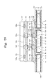
FIG. 20 is a sectional view of a semiconductor package according to a third example embodiment;
FIG. 21 is a sectional view of a semiconductor package according to a fourth example embodiment of the inventive concepts;
FIG. 22 is a sectional view of a semiconductor package according to a fifth example embodiment;
FIGS. 23 through 26 are manufacturing sectional views illustrating sequential manufacturing processes of a semiconductor package having a section of FIG. 22 according to an example embodiment of the inventive concepts;
FIG. 27 is a manufacturing sectional view illustrating sequential manufacturing processes of a semiconductor package having a section of FIG. 22 according to another example embodiment of the inventive concepts;
FIG. 28 is a view illustrating an example of a package module including a semiconductor package that the technique of the inventive concepts is applied;
FIG. 29 is a block diagram illustrating an example of an electronic device including a semiconductor package that the technique of the inventive concepts is applied; and
FIG. 30 is a block diagram illustrating a memory system with a semiconductor package that the technique of the inventive concepts is applied.
DETAILED DESCRIPTION OF THE EMBODIMENTS
Example embodiments will be described more fully hereinafter with reference to the accompanying drawings, in which example embodiments are shown. The present invention may, however, be embodied in many different forms and should not be construed as limited to example embodiments as set forth herein. Rather, example embodiments are provided so that this disclosure will be thorough and complete, and will fully convey the scope of the present invention to those skilled in the art. In the drawings, the sizes and relative sizes of layers and regions may be exaggerated for clarity.
It will be understood that when an element or layer is referred to as being “on,” “connected to” or “coupled to” another element or layer, it can be directly on, connected or coupled to the other element or layer or intervening elements or layers that may be present. In contrast, when an element is referred to as being “directly on,” “directly connected to” or “directly coupled to” another element or layer, there are no intervening elements or layers present. Like numerals refer to like elements throughout. As used herein, the term “and/or” includes any and all combinations of one or more of the associated listed items.
It will be understood that, although the terms first, second, third etc. may be used herein to describe various elements, components, regions, layers and/or sections, these elements, components, regions, layers and/or sections should not be limited by these terms. These terms are only used to distinguish one element, component, region, layer or section from another region, layer or section. Thus, a first element, component, region, layer or section discussed below could be termed a second element, component, region, layer or section without departing from the teachings of the present invention.
Spatially relative terms, such as “beneath,” “below,” “lower,” “above,” “upper” and the like, may be used herein for ease of description to describe one element or feature's relationship to another element(s) or feature(s) as illustrated in the figures. It will be understood that the spatially relative terms are intended to encompass different orientations of the device in use or operation in addition to the orientation depicted in the figures. For example, if the device in the figures is turned over, elements described as “below” or “beneath” other elements or features would then be oriented “above” the other elements or features. Thus, the exemplary term “below” can encompass both an orientation of above and below. The device may be otherwise oriented (rotated 90 degrees or at other orientations) and the spatially relative descriptors used herein interpreted accordingly.
The terminology used herein is for the purpose of describing example embodiments only and is not intended to be limiting of the present invention. As used herein, the singular forms “a,” “an” and “the” are intended to include the plural forms as well, unless the context clearly indicates otherwise. It will be further understood that the terms “comprises” and/or “comprising,” when used in this specification, specify the presence of stated features, integers, steps, operations, elements, and/or components, but do not preclude the presence or addition of one or more other features, integers, steps, operations, elements, components, and/or groups thereof.
Example embodiments are described herein with reference to cross-sectional illustrations that are schematic illustrations of idealized example embodiments (and intermediate structures). As such, variations from the shapes of the illustrations as a result, for example, of manufacturing techniques and/or tolerances, are to be expected. Thus, example embodiments should not be construed as limited to the particular shapes of regions illustrated herein but are to include deviations in shapes that result, for example, from manufacturing. For example, an implanted region illustrated as a rectangle will, typically, have rounded or curved features and/or a gradient of implant concentration at its edges rather than a binary change from implanted to non-implanted region. Likewise, a buried region formed by implantation may result in some implantation in the region between the buried region and the surface through which the implantation takes place. Thus, the regions illustrated in the figures are schematic in nature and their shapes are not intended to illustrate the actual shape of a region of a device and are not intended to limit the scope of the present invention.
Unless otherwise defined, all terms (including technical and scientific terms) used herein have the same meaning as commonly understood by one of ordinary skill in the art to which this invention belongs. It will be further understood that terms, such as those defined in commonly used dictionaries, should be interpreted as having a meaning that is consistent with their meaning in the context of the relevant art and will not be interpreted in an idealized or overly formal sense unless expressly so defined herein.
Example embodiments of the inventive concepts will be described below in more detail with reference to the accompanying drawings. The inventive concepts may, however, be embodied in different forms and should not be construed as limited to the example embodiments set forth herein. Rather, these example embodiments are provided so that this disclosure will be thorough and complete, and will fully convey the scope of the inventive concepts to those skilled in the art. In the drawings, the dimensions of layers and regions are exaggerated for clarity of illustration. It will also be understood that when a layer (or film) is referred to as being ‘on’ another layer or substrate, it can be directly on the other layer or substrate, or intervening layers may also be present. Further, it will be understood that when a layer is referred to as being ‘under’ another layer, it can be directly under, and one or more intervening layers may also be present. In addition, it will also be understood that when a layer is referred to as being ‘between’ two layers, it can be the only layer between the two layers, or one or more intervening layers may also be present. Like reference numerals refer to like elements throughout.
Embodiment 1
FIG. 1 is a plan view of a semiconductor package according to a first example embodiment (embodiment 1) of the inventive concepts. FIG. 2 is a sectional view taken along the line II-II′ of FIG. 1.
Referring to FIGS. 1 and 2, the semiconductor package 300 of the embodiment 1 includes a circuit substrate 100 and a semiconductor chip 200 mounted thereon. The circuit substrate 100 includes a base substrate 1. The base substrate 1 may be formed of Bismaleimide triazine resin, alumina based ceramic, glass based ceramic, or silicon.
The base substrate 1 includes a first side 2 a and a second side 2 b facing the first side 2 a. The base substrate 1 includes a via hole 5 penetrating the first side 2 a and the second side 2 b. A metal plate 3 is disposed on the first side 2 a and the second side 2 b, and a seed layer 7 is disposed on the metal plate 3 and the via hole 5. The metal plate 3 may be a copper plate. For example, the seed layer 7 may be formed of an electroless plating pattern. Electro plating patterns 9 a, 9 b, 9 c, and 9 d are disposed on the seed layer 7. The plating patterns 9 a, 9 b, 9 c, and 9 d may include a substrate connection terminal 9 a, a via metal pattern 9 b, a circuit metal pattern 9 c, and a ball land 9 d. The substrate connection terminal 9 a is disposed on the first side 2 a and is electrically connected to a chip connection terminal 122 of a semiconductor chip 200. The via metal pattern 9 b is disposed to cover an inner sidewall of the via hole 5. The circuit metal pattern 9 c is disposed on the first side 2 a and is electrically connected to the substrate connection terminal 9 a to deliver a signal. The ball land 9 d is disposed on the second side 2 b and an external solder ball 40 is attached on the ball land 9 d. The seed layer 7 and the electro plating patterns 9 a, 9 b, 9 c, and 9 d may include copper. A first substrate insulation layer 13 is disposed on the first side 2 a and a second substrate insulation layer 17 is disposed on the second side 2 b. The first substrate insulation layer 13 and the second substrate insulation layer 17 may correspond to a solder resist layer and may be formed of a photo sensitive photoresist layer. The first substrate insulation layer 13 includes a substrate connection terminal opening 15 a exposing the substrate connection terminal 9 a. The first substrate insulation layer 13 may further include dummy substrate openings 15 b and 15 c. The dummy substrate openings 15 b and 15 c may include a via dummy opening 15 b and a circuit dummy opening 15 c, which expose predetermined portions of the via metal pattern 9 b and the circuit metal pattern 9 c, respectively. The circuit dummy opening 15 c of this example embodiment has a rectangular line form on a plane but the inventive concepts is not limited thereto and thus the circuit dummy opening 15 c may have various plane forms along the circuit metal pattern 9 c. The second substrate insulation layer 17 may include a ball land opening 19 exposing the ball land 9 d. The dummy substrate openings 15 b and 15 c are filled with dummy solders 132 b and 132 c. The dummy solders 132 b and 132 c include a via dummy solder 132 b and a circuit dummy solder 132 c. The via dummy solder 132 b fills the via dummy opening 15 b and the circuit dummy solder 132 c fills the circuit dummy opening 15 c.
The semiconductor chip 200 is disposed on the circuit substrate 100. A chip connection terminal 122 is disposed at the bottom surface of the semiconductor chip 200. A chip insulation layer 124 with a chip connection terminal opening 135 a exposing the chip connection terminal 122 is provided at the bottom surface of the semiconductor chip 200. The chip connection terminal 122 is disposed at a portion overlapping the substrate connection terminal 9 a. An inner solder ball 133 is disposed between the chip connection terminal 122 and the substrate connection terminal 9 a so that it electrically connects the chip connection terminal 122 with the substrate connection terminal 9 a. The dummy solders 132 b and 132 c may be formed of the same material as the inner solder ball 133, which may be metals such as Pb, Sn, In, Bi, Sb, Ag, or combinations thereof. A resin layer 131 is disposed between the chip insulation layer 124 and the first substrate insulation layer 13 to protect the inner solder ball 133. No opening is provided in the chip insulation layer 124 at a position that the dummy solders 132 b and 132 c overlap. A molding layer 42 may cover the semiconductor chip 200 on the circuit substrate 100.
FIGS. 3 through 8, 9A, 10A, and 12 are manufacturing sectional views illustrating sequential manufacturing processes of a semiconductor package having a section of FIG. 2 according to an example embodiment of the inventive concepts.
Referring to FIG. 3, a base substrate 1 having a first side 2 a and a second side 2 b facing the first side 2 a is prepared. A metal plate 3 is stacked on the first side 2 a and the second side 2 b of the base substrate 1. The metal plate 3 may be fixed on the base substrate 1 through a bonding and/or compression method. The metal plate 3 may be a copper plate. A half-etching process may be performed to reduce a thickness of the metal plate 3.
Referring to FIG. 4, a via hole 5 penetrating the metal plate 3 and the base substrate 1 is formed through an etching and drill process.
Referring to FIG. 5, a seed layer 7 is formed on the base substrate 1 having the via hole 5. The seed layer 7 may be formed through an electroless plating method. The seed layer 7 may include copper. The seed layer 7 is formed to cover the metal plate 3 on the first side 2 a and the second side 2 b and an inner sidewall of the via hole 5.
Referring to FIG. 6, an electro plating layer 9 is formed on the seed layer 7. The electro plating layer 9 may be formed through an electro plating method. The electro plating layer 9 may include copper. The electro plating layer 9 is formed on the seed layer 7 so that it is formed on an inner sidewall of the via hole 5.
Referring to FIG. 7, a dry film is covered on the electro plating layer 9 and exposure and development processes are performed thereon to form a dry film mask 11. The dry film mask 11 may be formed to cover the via hole 5.
Referring to FIG. 8, by using the dry film mask 11 as an etch mask and etching the electro plating layer 9 therebelow, a substrate connection terminal 9 a, a via metal pattern 9 b, a circuit metal pattern 9 c, and a ball land 9 d are formed. The seed layer 7 and the metal plate 3 below the electrode plating layer 9 are etched simultaneously, so that a surface of the base substrate 1 is exposed. Then, the dry film mask 11 is removed. The dry film mask 11 may be removed through a wet etching method.
FIG. 9B is an enlarged perspective view of a portion A of FIG. 9A.
Referring to FIGS. 9A and 9B, a first substrate insulation layer 13 is formed on the first side 2 a of the base substrate 1 and a second substrate insulation layer 17 is formed on the second side 2 b. The substrate insulation layers 13 and 17 as a solder resist layer may be formed of a photo sensitive photoresist and also may be formed through a photolithography process. The first substrate insulation layer 13 is formed to have a substrate connection terminal opening 15 a exposing the substrate connection terminal 9 a. The first substrate insulation layer 13 is formed to include dummy substrate openings 15 b and 15 c. The dummy substrate openings 15 b and 15 c may include a via dummy opening 15 b and a circuit dummy opening 15 c exposing predetermined portions of the via metal pattern 9 b and the circuit metal pattern 9 c, respectively. The circuit dummy opening 15 c may be formed to have a width W1 that is broader than a width W2 of the circuit metal pattern 9 c as shown in FIG. 9B. Accordingly, a surface of the base substrate 1 adjacent to both sidewalls of the circuit metal pattern 9 c may be exposed through the circuit dummy opening 15 c. Additionally, the both sides of the circuit metal pattern 9 c may be exposed. A ball land opening 19 exposing the ball land 9 d may be formed in the second substrate insulation layer 17. Thus, a circuit substrate 10 may be completed.
FIG. 10B is an enlarged sectional view of a portion B of FIG. 10A.
Referring to FIGS. 10A, 10B, and 12, a mixture 134 including a solder particle 132 and an adhesive resin 130 is applied on the circuit substrate 100. The solder particle 132 and the adhesive resin 130 may be mixed with a volume ratio of about 1:9 to about 5:5 in the mixture 134. For example, the solder particle 132 may have a diameter of about 0.1 μm to about 100 μm. The solder particle 132 may be a particle of metals such as Cu, Pb, Sn, In, Bi, Sb, Ag, and combinations thereof. The adhesive resin 130 may have a flux function. Once heated, the adhesive resin 130 may have a function for removing an oxide layer on a surface of the solder particle 132. The adhesive resin 130 may have an adhesive function. The adhesive resin 130 may be an epoxy based resin, for example and may include bisphenol A and epichlorohydrin as more detailed example. The mixture 134 may further include a reductant, a deforming agent, a solvent and/or a hardener. The hardener may be silicon base, phenol base, acid anhydride base, and amine base. The mixture 134 may further include a thermal setting agent, a thermal plastic agent and/or a UV hardening material.
Like the above, after the mixture 134 is applied, a semiconductor chip 200 is provided on the mixture 134. Then, the circuit substrate 100 is heated. At this point, the circuit substrate 100 is heated at a temperature of more than a melting point of the solder particle 132. The heated adhesive resin 130 may remove an oxide layer on a surface of the solder particle 132. Moreover, the mixture 134 may include a deforming agent, the deforming agent may suppress gas generation in the mixture 134 so that it helps the solder particle 132 to reveal a wetting characteristic on a metal surface. The adhesive resin 130 is hardened after its solvent is evaporated through the heating process so that a resin layer 131 may be formed. Additionally, as shown in FIG. 10B, the solder particle 132, which flows along the dotted arrow in the adhesive resin 130, moves to and is attached to metal patterns (i.e., surfaces of the substrate connection terminal 9 a, the via metal pattern 9 b, the circuit metal pattern 9 c, and a chip connection terminal 122) exposed to openings 15 a, 15 b, and 15 c. Thus, an inner solder ball 133 is formed between the chip connection terminal 122 and the substrate connection terminal 9 a. Simultaneously, solder particles 132, which do not become the inner solder ball 133 connecting the substrate connection terminal 9 a with the chip connection terminal 122 and remain on a peripheral region, become a via dummy solder 132 b and a circuit dummy solder 132 c filling the via dummy opening 15 b and the circuit dummy opening 15 c, respectively. Since the circuit dummy opening 15 c is formed with a width W1 that is broader than a width W2 of the circuit metal pattern 9 c as shown in FIG. 9B, the solder particles 132 are attached to a top surface and both sidewalls of the exposed circuit metal pattern 9 c. Accordingly, since the circuit dummy opening 15 c is formed to have a width W1 broader than a width W2 of the circuit metal pattern 9 c, an area of the circuit metal pattern 9 c on which the solder particles 132 are attached broadens. Therefore, limitations such as electrical short and leakage current by remaining solder particles may be resolved so that a reliable semiconductor package may be provided. Moreover, since the dummy solders 132 b and 132 c are formed to fill the dummy openings 15 b and 15 c in the dummy openings 15 b and 15 c, they do not excessively protrude to the top surface of the first substrate insulation layer 13. Thus, compared to a case that a dummy solder is disposed on a substrate insulation layer without a dummy opening, according to the inventive concepts, top surfaces of the dummy solders 132 b and 132 c become far from the semiconductor chip 200. As a result, influences such as signal interference due to a coupling effect may be reduced. Therefore, a reliable semiconductor package may be realized.
Next, a molding layer 42 may be formed through a molding process.
FIG. 11A is a manufacturing sectional view illustrating a semiconductor package having a section of FIG. 2 according to another example embodiment of the inventive concepts. FIG. 11B is an enlarged sectional view of a portion C of FIG. 11A.
Referring to FIGS. 11A, 11B, and 12, a mixed multilayer 134 a (which may be called a solder foil) is provided on the circuit substrate 100 of FIG. 9A. The mixed multilayer 134 a includes a solder particle layer 132 a formed of a solder particle 132 (which will be described with reference to FIG. 10A) and an adhesive resin layer 130 a formed of an adhesive resin 130 (which will be described with reference to FIG. 10A) disposed on both sides of the solder particle layer 132 a. Also, the semiconductor chip 200 is provided on the mixed multilayer 134 a. The circuit substrate 100 is heated. The adhesive resin layer 130 a is hardened after its solvent is evaporated through the heating process so that a resin layer 131 may be formed. Additionally, as shown in FIG. 11B, the solder particle layer 132 a, which flows along the dotted arrow in the adhesive resin layer 130 a, moves to and is attached to metal patterns (i.e., surfaces of the substrate connection terminal 9 a, the via metal pattern 9 b, the circuit metal pattern 9 c, and a chip connection terminal 122) exposed to openings 15 a, 15 b, and 15 c. Thus, an inner solder ball 133 is formed between the chip connection terminal 122 and the substrate connection terminal 9 a. Simultaneously, the solder particle layer 132 a, which does not become the inner solder ball 133 connecting the substrate connection terminal 9 a with the chip connection terminal 122 and remains on a peripheral region, become a via dummy solder 132 b and a circuit dummy solder 132 c filling the via dummy opening 15 b and the circuit dummy opening 15 c, respectively. Therefore, limitations such as electrical short and leakage current by a remaining solder particle layer may be resolved so that a reliable semiconductor package may be provided. Additionally, a self-assembly solder bonding process for more simple flip chip bonding may be performed using the mixed multilayer 134 a.
According to an example embodiment of the inventive concepts, since a circuit dummy opening 15 c is formed to expose a predetermined portion of a circuit metal pattern (i.e., a signal transmission path), a dummy metal pattern may not need to be formed purposely. Thus, a signal wiring design of a circuit substrate may not need to be changed. Accordingly, without a change of the signal wiring design of the circuit substrate, only a circuit dummy opening of a substrate insulation layer is formed on a desired position so that a reliable semiconductor package may be realized.
Embodiment 2
FIG. 13 is a plan view of a semiconductor package according to a second example embodiment (embodiment 2) of the inventive concepts. FIG. 14A is a sectional view taken along the line XIVA-XIVA′ of FIG. 13. FIG. 14B is a sectional view taken along the line XIVB-XIVB′ of FIG. 13.
Referring to FIGS. 13, 14A and 14B, a substrate dummy metal pattern 9 f and a recess metal pattern 9 e are additionally disposed on a first side 2 a of a circuit substrate 101 in a semiconductor package 301 according to the embodiment 2. The substrate dummy metal pattern 9 f may be disposed between two adjacent substrate connection terminals 9 a. A recessed region 5 a is formed in a base substrate 1 of the circuit substrate 101 and the recess metal pattern 9 e is disposed in the recessed region 5 a thereby filling the recessed region 5 a. The recess metal pattern 9 e may be disposed between two adjacent substrate connection terminals 9 a and between two adjacent substrate dummy metal patterns 9 f. The positions of the substrate dummy metal pattern 9 f and the recess metal pattern 9 e are not limited thereto and may vary. A first substrate insulation layer 13 is disposed on the first side 2 a. A substrate connection terminal opening 15 a and dummy openings 15 b, 15 c, 15 e, and 15 f are formed in the first substrate insulation layer 13. The dummy openings 15 b, 15 c, 15 e, and 15 f may include a via dummy opening 15 b, a circuit dummy opening 15 c, a recess dummy opening 15 e, and a substrate dummy opening 15 f, which expose predetermined portions of a via metal pattern 9 b, a circuit metal pattern 9 c, a recess metal pattern 9 e, and a substrate dummy metal pattern 9 f, respectively. The dummy openings 15 b, 15 c, 15 e, and 15 f may be filled with a via dummy solder 132 b, a circuit dummy solder 132 c, a recess dummy solder 132 e, and a substrate dummy solder 132 f, respectively. Besides that, configurations may be identical/similar to those of the embodiment 1.
FIGS. 15A through 19A are manufacturing sectional views illustrating sequential manufacturing processes of a semiconductor package having a section of FIG. 14A. FIGS. 15B through 19B are manufacturing sectional views illustrating sequential manufacturing processes of a semiconductor package having a section of FIG. 14B.
Referring to FIGS. 15A and 15B, a base substrate 1 including a first side 2 a and a second side 2 b facing the first side 2 a is prepared. A metal plate 3 may be stacked on the first side 2 a and the second side 2 b of the base substrate 1. The metal plate 3 may be a copper plate. A half-etching process may be performed to reduce a thickness of the metal plate 3. A via hole 5 penetrating the metal plate 3 and the base substrate 1 is formed through etching and drill processes. At this point, a recessed region 5 a is formed by removing predetermined portions of the metal plate 3 and the base substrate 1. The via hole 5 and the recessed region 5 a may be simultaneously or separately formed.
Referring to FIGS. 16A and 16B, a seed layer 7 is formed on the base substrate 1 having the via hole 5 and the recessed region 5 a. The seed layer 7 may be formed through an electroless plating method. The seed layer 7 may include copper. The seed layer 7 is formed to cover the metal plate 3 on the first side 2 a and the second sides 2 b, an inner sidewall of the via hole 5, and the inner sidewall and the bottom of the recessed region 5 a. An electro plating layer 9 is formed on the seed layer 7. The electro plating layer 9 may be formed through an electro plating method. The electro plating layer 9 may include copper. Since the electro plating layer 9 is formed on the seed layer 7, it is formed on the inner sidewall of the via hole 5 and the inner sidewall and the bottom of the recessed region 5 a.
Referring to FIGS. 17A and 17B, by etching the electro plating layer 9 using a dry film mask as an etch mask, a substrate connection terminal 9 a, a via metal pattern 9 b, a circuit metal pattern 9 c, a ball land 9 d, a recess metal pattern 9 e, and a substrate dummy metal pattern 9 f are formed. The seed layer 7 and the metal plate 3 below the electrode plating layer 9 are etched simultaneously so that a surface of the base substrate 1 is exposed. Then, the dry film mask is removed.
FIG. 18C is an enlarged perspective view of a portion D of FIG. 18A.
Referring to FIGS. 18A, 18B, and 18C, a first substrate insulation layer 13 is formed on the first side 2 a of the base substrate 1, and a second substrate insulation layer 17 is formed on the second side 2 b. The substrate insulation layers 13 and 17 as a solder resist layer may be formed of a photo sensitive photoresist and also may be formed through a photolithography process. The first substrate insulation layer 13 is formed to have a substrate connection terminal opening 15 a exposing the substrate connection terminal 9 a. The first substrate insulation layer 13 is formed to include dummy substrate openings 15 b, 15 c, 15 e, and 15 f. The dummy substrate openings 15 b, 15 c, 15 e, and 15 f may include a via dummy opening 15 b, a circuit dummy opening 15 c, a recess dummy opening 15 e, and a substrate dummy opening 15 f exposing predetermined portions of the via metal pattern 9 b, the circuit metal pattern 9 c, the recess metal pattern 9 e, and the substrate dummy metal pattern 9 f, respectively. The substrate dummy opening 15 f may be formed to have a width W3 that is broader than a width W4 of the substrate dummy metal pattern 9 f as shown in FIG. 18C. Accordingly, a surface of the base substrate 1 adjacent to both sidewalls of the substrate dummy metal pattern 9 f may be exposed through the substrate dummy opening 15 f. Additionally, three sides of the substrate dummy metal pattern 9 f may be exposed. A ball land opening 19 exposing the ball land 9 d may be formed in the second substrate insulation layer 17. Thus, a circuit substrate 101 may be completed.
Referring to FIGS. 19A and 19B, a mixture 134 including a solder particle 132 and an adhesive resin 130 is applied on the circuit substrate 101. After the mixture 134 is applied, a semiconductor chip 200 is provided on the mixture 134. Then, the circuit substrate 100 is heated. At this point, the circuit substrate 100 is heated at a temperature of more than a melting point of the solder particle 132. Therefore, referring to FIGS. 14A and 14B, the adhesive resin 130 is hardened after its solvent is evaporated through the heating process so that a resin layer 131 may be formed. Additionally, the solder particle 132, which flows in the adhesive resin 130, moves to and is attached to metal patterns (i.e., surfaces of the substrate connection terminal 9 a, the via metal pattern 9 b, the circuit metal pattern 9 c, the recess metal pattern 9 e, the substrate dummy metal pattern 9 f, the chip connection terminal 122) exposed to openings 15 a, 15 b, 15 c, 15 e, and 15 f. Thus, an inner solder ball 133 is formed between the chip connection terminal 122 and the substrate connection terminal 9 a. Simultaneously, solder particles 132, which do not become the inner solder ball 133 connecting the substrate connection terminal 9 a with the chip connection terminal 122 and remain on a peripheral region, become a via dummy solder 132 b, a circuit dummy solder 132 c, a recess dummy solder 132 e, and a substrate dummy solder 132 f filling the dummy opening 15 b, 15 c, 15 e, and 15 f, respectively.
As described with reference to FIG. 11A, a self-assembly solder bonding process may be performed using the mixed multilayer. Its forming process may be identical/similar to that of the embodiment 1.
In this example embodiment, there is a change of a signal wiring design of a circuit substrate according to an addition of a substrate dummy metal pattern and a recess metal pattern. However, according to this example embodiment, since dummy openings are formed in the first substrate insulation layer to allow the dummy solders to fill the dummy openings, a reliable semiconductor package described in the embodiment 1 may be realized.
Embodiment 3
FIG. 20 is a sectional view of a semiconductor package according to a third example embodiment (embodiment 3).
Referring to FIG. 20, in relation to the semiconductor package 302 according to the embodiment 3, a chip connection terminal 122 and a chip dummy metal pattern 126 are disposed at the bottom surface of a semiconductor chip 200 mounted on a circuit substrate 102. Then, a chip insulation layer 124, which includes a chip connection terminal opening 135 a exposing the chip connection terminal 122 and a chip dummy opening 135 g exposing the chip dummy metal pattern 126 is provided at the bottom surface of the semiconductor chip 200. The chip dummy opening 135 g is filled with a chip dummy solder 132 g. This may be the feature of this example embodiment.
Selectively, a first substrate insulation layer 13 having a substrate dummy metal pattern 132 f and a substrate dummy opening 15 f exposing the same may be disposed on the circuit substrate 102. The positions of the chip dummy opening 135 g and the substrate dummy opening 15 f may not overlap each other. The first substrate insulation layer 13 does not expose a circuit metal pattern 9 c and a via metal pattern 9 b. Unlike the embodiment 2 (in which the via hole 5 is filled with the via dummy solder 132 b), according to this example embodiment, the via hole 5 may be filled with a conductive paste 21.
The circuit substrate 102 of this example embodiment may be replaced with the circuit substrate 100 of the embodiment 1. Besides that, a configuration and a manufacturing method may be identical/similar to those of the embodiment 1.
Embodiment 4
FIG. 21 is a sectional view of a semiconductor package according to a fourth example embodiment (embodiment 4) of the inventive concepts.
Referring to FIG. 21, in relation to the semiconductor package 303 according to this example embodiment, a bump 128 is attached to a chip connection terminal 122 disposed at the bottom surface of a semiconductor chip 200 mounted on a circuit substrate 103. An inner solder ball 133 connecting the chip connection terminal 122 with a substrate connection terminal 9 a electrically is formed to cover at least a side of the bump 128. The inner solder ball 133 may cover the bottom of the bump 128.
During a self-assembly solder bonding process in forming processes of the semiconductor package 303, the side and the bottom of the bump 128 are exposed so that an area to which solder particles are attached is increased. As a result, the adhesiveness between an inner solder ball 133 and the bump 128 may be improved. Additionally, due to the height of the bump 128, an interval between the semiconductor chip 200 and the circuit substrate 103 may be uniformly maintained. Thus, a reliable semiconductor package may be realized. In this example embodiment, the circuit substrate 103 may be identical to that 101 of the embodiment 2. Besides that, a configuration and a manufacturing method may be identical/similar to those of the embodiments 1 to 3.
Embodiment 5
FIG. 22 is a sectional view of a semiconductor package according to a fifth example embodiment (embodiment 5).
Referring to FIG. 22, in relation to the semiconductor package 304 of the embodiment 4, more than two semiconductor chips 200 and 201 are stacked and mounted on a circuit substrate 104. That is, the lower semiconductor chip 201 is stacked on the circuit substrate 104 and the upper semiconductor chip 202 is stacked on the lower semiconductor chip 201. A through via 142 penetrating the inside may be formed in the lower semiconductor chip 201. A first lower chip connection terminal 146 contacting the bottom of the through via 142 and a first lower chip insulation layer 148 exposing the first lower chip connection terminal 146 are disposed at the bottom surface of the lower semiconductor chip 201. A second lower chip connection terminal 144 contacting the top of the through via 142 and a second lower chip insulation layer 149 exposing the second lower chip connection terminal 144 are disposed on the top surface of the lower semiconductor chip 201. An upper chip connection terminal 122 and an upper chip dummy metal pattern 126 are disposed at the bottom of the upper semiconductor chip 202. Also, an upper chip insulation layer 124 exposing the upper chip connection terminal 122 and the upper chip dummy metal pattern 126 is disposed at the bottom of the upper semiconductor chip 202. An upper chip dummy solder 152 g is attached to the upper chip dummy metal pattern 126. A first inner solder ball 133 is disposed between the first lower chip connection terminal 146 and a substrate connection terminal 9 a of the circuit substrate 104. A second inner solder ball 152 a is disposed between the upper chip connection terminal 122 and the second lower chip connection terminal 144.
The circuit substrate 104 of this example embodiment may be identical/similar to circuit substrate 101 as shown in FIG. 14. Additionally, the chip dummy metal pattern 126 is disposed on the bottom surface of the semiconductor chip 202 but may be disposed at the top surface or the bottom surface of the lower semiconductor chip 201. When the chip dummy metal pattern 126 is disposed at the bottom surface of the lower semiconductor chip 201, it may be disposed at a position that do not overlap dummy openings 15 a, 15 b, 15 c, and 15 f of the circuit substrate 104.
FIGS. 23 through 26 are manufacturing sectional views illustrating sequential manufacturing processes of a semiconductor package having a section of FIG. 22 according to an example embodiment of the inventive concepts.
Referring to FIG. 23, a first mixed multilayer 134 a is provided on a circuit substrate 104. The first mixed multilayer 134 a includes a first solder particle layer 132 a formed of the solder particle 132 of FIG. 10A and a first adhesive resin layer 130 a disposed at the both sides of the first solder particle layer 132 a and formed of the adhesive resin 130 of FIG. 10A. Also, a lower semiconductor chip 201 is provided on the first mixture multilayer 134 a.
Referring to FIG. 24, the circuit substrate 100 is heated. The first adhesive resin layer 130 a is hardened after its solvent is evaporated through the heating process so that a first resin layer 131 may be formed. The first solder particle layer 132 a moves to and is attached to metal patterns (i.e., surfaces of the substrate connection terminal 9 a, the via metal pattern 9 b, the circuit metal pattern 9 c, the substrate dummy metal pattern 9 f, and the first lower chip connection terminal 146) exposed to openings 15 a, 15 b, 15 c, and 15 f in the adhesive resin layer 130 a. Therefore, a first inner solder ball 133 is formed between the first lower chip connection terminal 146 and the substrate connection terminal 9 a. Simultaneously, the solder particle layer 132 a, which does not become the first inner solder ball 133 connecting the substrate connection terminal 9 a with the first lower chip connection terminal 146 and remains on a peripheral region, becomes a via dummy solder 132 b, a circuit dummy solder 132 c, and a substrate dummy solder 132 f filling the dummy opening 15 b, 15 c, and 15 f, respectively.
Referring to FIG. 25, a second mixed multilayer 154 is provided on the lower semiconductor chip 201. The second mixed multilayer 154 includes a second solder particle layer 152 formed of the solder particle 132 of FIG. 10A and a second adhesive resin layer 150 disposed at the both sides of the second solder particle layer 152 and formed of the adhesive resin 130 of FIG. 10A. Also, an upper semiconductor chip 202 is provided on the second mixture multilayer 154.
Referring to FIG. 26, the circuit substrate 100 is heated. The second adhesive resin layer 150 is hardened after its solvent is evaporated through the heating process so that a second resin layer 151 may be formed. The second solder particle layer 152 moves to and is attached to metal patterns (i.e., surfaces of the second lower chip connection terminal 144, the upper chip connection terminal 122, and the upper chip dummy metal pattern 126). Therefore, a second inner solder ball 152 a is formed between the second lower chip connection terminal 144 and the upper chip connection terminal 122 and an upper chip dummy solder 152 g is formed in the upper chip dummy metal pattern 126.
Next, after an external solder ball 40 is attached and a molding layer 42 is formed, a semiconductor package 304 having a section of FIG. 22 may be completed.
FIG. 27 is a manufacturing sectional view illustrating sequential manufacturing processes of a semiconductor package having a section of FIG. 22 according to another example embodiment of the inventive concepts.
Referring to FIG. 27, a first mixed multilayer 134 a, a lower semiconductor chip 201, a second mixed multilayer layer 154, and an upper semiconductor chip 202 are sequentially stacked on a circuit substrate 104. Then, the circuit board 104 is heated so that a structure having a section of FIG. 26 may be manufactured more simply.
Although a mixed multilayer is used in the manufacturing method of this example embodiment, as described with reference to FIGS. 10A, 10B, and 12, a mixture 134 is applied for the next process. When the lower semiconductor chip 201 is joined to the upper semiconductor chip 202 simultaneously using the mixture 134, the lower semiconductor chip 201 and the upper semiconductor chip 202 may be stacked when a solvent is volatized by hardening the mixture 134.
Although a semiconductor chip is mounted on a circuit substrate and an external solder ball 40 is attached to the circuit substrate in the semiconductor packages in the embodiments 1 through 5, the circuit substrate itself may correspond to a mother board and thus the external solder ball 40 may not be attached.
The semiconductor package technique may be applied to various kinds of semiconductor devices and a package module including the same.
FIG. 28 is a view illustrating an example of a package module including a semiconductor package that the technique of the inventive concepts is applied. Referring to FIG. 28, the package module 1200 may include a semiconductor integrated circuit chip 1220 and a Quad Flat Package (QFP) applied semiconductor integrated circuit chip 1230. As the semiconductor devices 1220 and 1230 to which a semiconductor package technique of the inventive concepts is applied are mounted on a substrate 1210, the package module 1200 may be formed. The package module 1200 may be connected to an external electronic device through an external connection terminal 1240 at one side of the substrate 1210.
The above semiconductor package technique may be applied to an electronic system. FIG. 29 is a block diagram illustrating an example of an electronic device including a semiconductor package that the technique of the inventive concepts is applied. Referring to FIG. 29, the electronic system 1300 may include a controller 1310, an input/output device (or I/O) 1320 such as a keypad, a keyboard, and a display, and a memory device 1330. The controller 1310, the input/output device 1320, and the memory device 1330 may be combined through a bus 1350. The bus 1350 is a path through which data transfers. For example, the controller 1310 may include at least one micro processor, digital signal processor, micro controller, or other processors similar thereto. The controller 1310 and the memory device 1330 may include a semiconductor package according to the inventive concepts. The input/output device 1320 may include a keyboard, a keypad, or a display device. The memory device 1330 stores data. The memory device 1330 may store data and/or commands executed by the controller 1310. The memory device 1330 may include a volatile memory device and/or a nonvolatile memory device. Or, the memory device 1310 may be formed of a flash memory. For example, a flash memory to which the technique of the inventive concepts is applied may be mounted on an information processing system such as a mobile device or a desktop computer. This flash memory may include a semiconductor disk device (SSD). In this case, the electronic system 1300 may stably store a large amount of data in the flash memory system. The electronic system 1300 may further include an interface 1340 for transmitting or receiving data to or from a network. The interface 1349 may have a wire/wireless form. For example, the interface 1340 may include an antenna or a wire/wireless transceiver. Although not shown in the drawings, it is apparent to those skilled in the art that the electronic system 1300 may further include an application chipset, a camera image processor (CIS), and an input/output device.
The electronic system 1300 may be realized with a mobile system, a personal computer, an industrial computer, or a system performing various functions. For example the mobile system may be a personal digital assistant (PDA), a portable computer, a web tablet, a mobile phone, a wireless phone, a laptop computer, a memory card, a digital music system, or an information transmitting/receiving system. If the electronic system 1300 is a device for wireless communication, it may use a communication interface protocol of the third generation communication system such as code division multiple access (CDMA), global system for mobile communications (GSM), enhanced-time division multiple access (E-TDMA), wideband code division multiple access (W-CDMA), and CDMA1000.
A semiconductor device to which the technique of the inventive concepts is applied may be provided with a form of a memory card. FIG. 30 is a block diagram illustrating a memory system with a semiconductor package that the technique of the inventive concepts is applied. Referring to FIG. 30, the memory card 1400 includes a non-volatile memory device 1410 and a memory controller 1420. The non-volatile memory device 1410 and the memory controller 1420 may store data or read the stored data. The non-volatile memory device 1410 may include at least one of the non-volatile memory devices that the technique of the inventive concepts is applied. The memory controller 1420 may control the flash memory device 1410 to read stored data or store data in response to a read/write request from a host. The memory card 1400 may interface with a host 1430 that may use the memory card 1400 to store or retrieve data.
According to an example embodiment of the inventive concepts, at least one of a substrate insulation layer and a chip insulation layer includes a dummy opening. During a self-assembly solder bonding process for flip chip bonding, dummy solder is formed by filling the dummy opening with solder particles, which do not become an inner solder ball and thus remain on a peripheral region. Thus, compared to a case that a dummy solder is disposed on a substrate insulation layer without a dummy opening, according to the inventive concepts, a top surface of a dummy solder does not protrude excessively, so that it becomes far from the semiconductor chip. As a result, influences such as signal interference due to a coupling effect may be reduced. Therefore, limitations such as electrical short and leakage current by remaining solder particles may be resolved so that a reliable semiconductor package may be provided.
According to an example embodiment of the inventive concepts, since a circuit dummy opening is formed to expose a predetermined portion of a circuit metal pattern (i.e., a signal transmission path), a dummy metal pattern may not need to be formed purposely. Thus, a signal wiring design of a circuit substrate may not need to be changed. Accordingly, without a change of the signal wiring design of the circuit substrate, only a circuit dummy opening of a substrate insulation layer is formed on a desired position so that a reliable semiconductor package may be realized.
The above-disclosed subject matter is to be considered illustrative and not restrictive, and the appended claims are intended to cover all such modifications, enhancements, and other example embodiments, which fall within the true spirit and scope of the inventive concepts. Thus, to the maximum extent allowed by law, the scope of the inventive concepts is to be determined by the broadest permissible interpretation of the following claims and their equivalents, and shall not be restricted or limited by the foregoing detailed description.

Claims (19)

What is claimed is:
1. A method of manufacturing a semiconductor package, the method comprising:
forming a circuit substrate including a base substrate, a substrate connection terminal on the base substrate, and a substrate insulation layer covering the base substrate and exposing the substrate connection terminal;
forming a mixture layer on the circuit substrate, the mixture layer including an adhesive resin and a plurality of solder particles;
providing a first semiconductor chip on the mixture layer, the first semiconductor chip including a chip connection terminal and a chip insulation layer exposing the chip connection terminal;
forming an inner solder ball between the substrate connection terminal and the chip connection terminal; and
forming a dummy solder in a dummy opening, the dummy opening being in one of the substrate insulation layer and the chip insulation layer, the dummy solder configured to be physically spaced apart from one of the circuit substrate and the first semiconductor chip.
2. The method of claim 1, wherein the solder particles are dispersed in the adhesive resin.
3. The method of claim 1, wherein the forming a mixture layer comprises providing a mixed multilayer including an adhesive resin layer formed of the adhesive resin and a solder particle layer formed of the solder particles.
4. The method of claim 1, wherein at least one of the forming a dummy solder and the forming an inner solder ball comprises heating the mixture layer to a temperature of more than a melting point of the solder particles.
5. The method of claim 1, wherein the forming a circuit substrate comprises:
preparing the base substrate;
forming the substrate connection terminal on the base substrate; and
forming the substrate insulation layer on the base substrate, the substrate insulation layer being formed to expose the substrate connection terminal.
6. The method of claim 5, further comprising:
forming a circuit metal pattern on the base substrate, wherein the substrate insulation layer includes the dummy opening and the dummy opening exposes the circuit metal pattern.
7. The method of claim 6, wherein the dummy opening has a greater width than a width of the circuit metal pattern.
8. The method of claim 5, further comprising:
forming a via hole by patterning the base substrate; and
forming a via metal pattern on a sidewall of the via hole, wherein the substrate insulation layer includes the dummy opening and the dummy opening exposes the via metal pattern.
9. The method of claim 5, further comprising:
forming a recessed region in the base substrate; and
forming a recess metal pattern covering a sidewall and a bottom of the recessed region,
wherein the substrate insulation layer is formed to have a dummy opening exposing the recess metal pattern.
10. The method of claim 5, further comprising:
forming a substrate dummy metal pattern on the base substrate, wherein the substrate insulation layer is formed to have the dummy opening and the dummy opening is formed to expose the substrate dummy metal pattern.
11. The method of claim 10, wherein the dummy opening is formed to have a width greater than a width of the substrate dummy metal pattern.
12. The method of claim 1, further comprising:
forming an upper mixture layer on the first semiconductor chip;
providing a second semiconductor chip on the upper mixture layer, the second semiconductor chip including an upper chip connection terminal and an upper chip insulation layer exposing the upper chip connection terminal; and
forming an upper inner solder ball between the chip connection terminal and the upper chip connection terminal.
13. The method of claim 12, wherein the forming an inner solder ball and the forming of the upper inner solder ball are performed simultaneously.
14. A method of manufacturing a semiconductor package, the method comprising:
forming at least one dummy opening in at least one of an insulation layer of a semiconductor chip and an insulation layer of a substrate;
forming an inner solder ball between the substrate and the semiconductor chip, the inner solder ball electrically connecting a chip connecting terminal of the semiconductor chip to a substrate connection terminal of the substrate;
forming a dummy solder in the at least one dummy opening, the dummy solder configured to be physically spaced apart from one of the substrate and the semiconductor chip.
15. The method of claim 14, further comprising:
forming at least one of a circuit metal pattern, a via metal pattern, and a dummy substrate metal pattern on the substrate, wherein
the at least one dummy opening is formed to expose at least one of the circuit metal pattern, the via metal pattern, and the dummy substrate metal pattern.
16. The method of claim 14, further comprising:
forming a circuit metal pattern, a via metal pattern, and a dummy substrate metal pattern on the substrate, wherein
the at least one dummy opening is a plurality of dummy openings formed to expose the circuit metal pattern, the via metal pattern, and the dummy substrate metal pattern.
17. The method of claim 14, further comprising:
forming a mixture layer on the substrate, the mixture layer including an adhesive resin and a plurality of solder particles, wherein
the inner solder ball and the dummy solder are simultaneously formed by heating the mixture layer.
18. The method of claim 17, wherein the solder particles are dispersed in the adhesive resin.
19. The method of claim 17, wherein the forming a mixture layer comprises providing a mixed multilayer including an adhesive resin layer formed of the adhesive resin and a solder particle layer formed of the solder particles.
US13/227,889 2010-10-20 2011-09-08 Semiconductor package and method of manufacturing the same Active 2031-10-19 US8673688B2 (en)

Applications Claiming Priority (2)

Application Number Priority Date Filing Date Title
KR1020100102563A KR101711499B1 (en) 2010-10-20 2010-10-20 Semiconductor package and method of forming the same
KR10-2010-0102563 2010-10-20

Publications (2)

Publication Number Publication Date
US20120100671A1 US20120100671A1 (en) 2012-04-26
US8673688B2 true US8673688B2 (en) 2014-03-18

Family

ID=45973369

Family Applications (1)

Application Number Title Priority Date Filing Date
US13/227,889 Active 2031-10-19 US8673688B2 (en) 2010-10-20 2011-09-08 Semiconductor package and method of manufacturing the same

Country Status (4)

Country Link
US (1) US8673688B2 (en)
JP (1) JP2012089847A (en)
KR (1) KR101711499B1 (en)
CN (1) CN102456658B (en)

Families Citing this family (12)

* Cited by examiner, † Cited by third party
Publication number Priority date Publication date Assignee Title
US9553040B2 (en) 2012-03-27 2017-01-24 Mediatek Inc. Semiconductor package
US20140001622A1 (en) 2012-06-27 2014-01-02 Infineon Technologies Ag Chip packages, chip arrangements, a circuit board, and methods for manufacturing chip packages
KR101917221B1 (en) * 2012-06-29 2018-11-13 엘지이노텍 주식회사 Camera module
JP2014072494A (en) * 2012-10-01 2014-04-21 Toshiba Corp Semiconductor device and method of manufacturing the same
TWI480989B (en) * 2012-10-02 2015-04-11 矽品精密工業股份有限公司 Semiconductor package and fabrication method thereof
KR20140081193A (en) * 2012-12-21 2014-07-01 삼성전기주식회사 Hybrid substrate with high density and low density substrate area and manufacturing method thereof
KR102111739B1 (en) * 2013-07-23 2020-05-15 삼성전자주식회사 Semiconductor package and method of manufacturing the same
TWI514530B (en) * 2013-08-28 2015-12-21 Via Tech Inc Circuit substrate, semiconductor package and process for fabricating a circuit substrate
TWI553807B (en) * 2014-06-13 2016-10-11 思鷺科技股份有限公司 Package structure
KR20160080526A (en) * 2014-12-29 2016-07-08 삼성전기주식회사 Printed circuit board and method of manufacturing the same
KR101665242B1 (en) * 2015-03-20 2016-10-11 앰코 테크놀로지 코리아 주식회사 Semiconductor package and manufacturing method thereof
CN113130457A (en) * 2019-12-31 2021-07-16 Tcl集团股份有限公司 Light source plate, preparation method thereof and display

Citations (8)

* Cited by examiner, † Cited by third party
Publication number Priority date Publication date Assignee Title
US20060055028A1 (en) * 2004-09-10 2006-03-16 Kabushiki Kaisha Toshiba Semiconductor device
WO2006030674A1 (en) 2004-09-15 2006-03-23 Matsushita Electric Industrial Co., Ltd. Flip chip mounting method and flip chip mounting element
US20060231949A1 (en) * 2005-04-14 2006-10-19 Chang-Yong Park Semiconductor module and method of forming a semiconductor module
WO2006123554A1 (en) 2005-05-17 2006-11-23 Matsushita Electric Industrial Co., Ltd. Flip-chip mounting body and flip-chip mounting method
JP2008078238A (en) 2006-09-19 2008-04-03 Nec Corp Structure and method for mounting electronic component
US20080311701A1 (en) * 2007-06-18 2008-12-18 Seung Taek Yang Method for fabricating semiconductor package
US20100052189A1 (en) * 2006-11-28 2010-03-04 Daisuke Sakurai Electronic component mounting structure and method for manufacturing the same
US20120098123A1 (en) * 2010-10-26 2012-04-26 Taiwan Semiconductor Manufacturing Company, Ltd. Molded Chip Interposer Structure and Methods

Family Cites Families (8)

* Cited by examiner, † Cited by third party
Publication number Priority date Publication date Assignee Title
JP3678547B2 (en) * 1997-07-24 2005-08-03 ソニーケミカル株式会社 Multilayer anisotropic conductive adhesive and method for producing the same
CN100563001C (en) * 2005-03-07 2009-11-25 松下电器产业株式会社 Fixing body and manufacture method thereof
WO2006098268A1 (en) * 2005-03-16 2006-09-21 Matsushita Electric Industrial Co., Ltd. Method of bump forming and method of flip chip mounting using conductive grain
JP4401411B2 (en) * 2005-03-17 2010-01-20 パナソニック株式会社 Mounting body provided with semiconductor chip and manufacturing method thereof
EP2055756A1 (en) * 2006-08-25 2009-05-06 Sumitomo Bakelite Company, Ltd. Adhesive tape, joint structure, and semiconductor package
US20090057378A1 (en) * 2007-08-27 2009-03-05 Chi-Won Hwang In-situ chip attachment using self-organizing solder
JP5560713B2 (en) * 2007-10-05 2014-07-30 日本電気株式会社 Electronic component mounting method, etc.
JP5264585B2 (en) * 2009-03-24 2013-08-14 パナソニック株式会社 Electronic component joining method and electronic component

Patent Citations (13)

* Cited by examiner, † Cited by third party
Publication number Priority date Publication date Assignee Title
US20060055028A1 (en) * 2004-09-10 2006-03-16 Kabushiki Kaisha Toshiba Semiconductor device
US20080017995A1 (en) 2004-09-15 2008-01-24 Seiji Karashima Flip Chip Mounting Process and Flip Chip Assembly
WO2006030674A1 (en) 2004-09-15 2006-03-23 Matsushita Electric Industrial Co., Ltd. Flip chip mounting method and flip chip mounting element
KR20070052791A (en) 2004-09-15 2007-05-22 마츠시타 덴끼 산교 가부시키가이샤 Flip chip mounting method and flip chip mounting element
JP3955302B2 (en) 2004-09-15 2007-08-08 松下電器産業株式会社 Method of manufacturing flip chip mounting body
US20060231949A1 (en) * 2005-04-14 2006-10-19 Chang-Yong Park Semiconductor module and method of forming a semiconductor module
WO2006123554A1 (en) 2005-05-17 2006-11-23 Matsushita Electric Industrial Co., Ltd. Flip-chip mounting body and flip-chip mounting method
US20090085227A1 (en) 2005-05-17 2009-04-02 Matsushita Electric Industrial Co., Ltd. Flip-chip mounting body and flip-chip mounting method
JP4402718B2 (en) 2005-05-17 2010-01-20 パナソニック株式会社 Flip chip mounting method
JP2008078238A (en) 2006-09-19 2008-04-03 Nec Corp Structure and method for mounting electronic component
US20100052189A1 (en) * 2006-11-28 2010-03-04 Daisuke Sakurai Electronic component mounting structure and method for manufacturing the same
US20080311701A1 (en) * 2007-06-18 2008-12-18 Seung Taek Yang Method for fabricating semiconductor package
US20120098123A1 (en) * 2010-10-26 2012-04-26 Taiwan Semiconductor Manufacturing Company, Ltd. Molded Chip Interposer Structure and Methods

Also Published As

Publication number Publication date
JP2012089847A (en) 2012-05-10
US20120100671A1 (en) 2012-04-26
CN102456658A (en) 2012-05-16
KR20120041010A (en) 2012-04-30
KR101711499B1 (en) 2017-03-13
CN102456658B (en) 2016-12-21

Similar Documents

Publication Publication Date Title
US8673688B2 (en) Semiconductor package and method of manufacturing the same
US8399992B2 (en) Package-on-package type semiconductor package
KR101862496B1 (en) Microelectronic package having a passive microelectronic device disposed within a package body, method of fabricating it and computing device comprising it
US8759958B2 (en) Semiconductor package and method of manufacturing the same
US7453155B2 (en) Method for fabricating a flip chip package
US20130295725A1 (en) Semiconductor package and method of forming the same
US20110207266A1 (en) Printed circuit board (pcb) including a wire pattern, semiconductor package including the pcb, electrical and electronic apparatus including the semiconductor package, method of fabricating the pcb, and method of fabricating the semiconductor package
CN104253115A (en) Underfill material flow control for reduced die-to-die spacing in semiconductor packages
KR20120016925A (en) Semiconductor package and method for manufacturing the same
US8513793B2 (en) Stacked semiconductor package and method of fabricating the same
US8981543B2 (en) Semiconductor package and method of forming the same
US9837360B2 (en) Wafer level packages and electronics system including the same
US9806066B2 (en) Semiconductor package including exposed connecting stubs
US20120068350A1 (en) Semiconductor packages, electronic devices and electronic systems employing the same
CN205248255U (en) Encapsulation stack type stacked package
US9460990B1 (en) Substrates and semiconductor packages including the same, electronic systems including the semiconductor packages, and memory cards including the semiconductor packages
US8304876B2 (en) Semiconductor package and method for manufacturing the same
US20130161784A1 (en) Semiconductor package
US20120087099A1 (en) Printed Circuit Board For Board-On-Chip Package, Board-On-Chip Package Including The Same, And Method Of Fabricating The Board-On-Chip Package
US9905540B1 (en) Fan-out packages including vertically stacked chips and methods of fabricating the same
US6689637B2 (en) Method of manufacturing a multi-chip semiconductor package
US9875990B2 (en) Semiconductor package including planar stacked semiconductor chips
US8828795B2 (en) Method of fabricating semiconductor package having substrate with solder ball connections
US20230057061A1 (en) Semiconductor chip
US20230034877A1 (en) Methods of manufacturing semiconductor device with bump interconnection

Legal Events

Date Code Title Description
AS Assignment

Owner name: SAMSUNG ELECTRONICS CO., LTD., KOREA, REPUBLIC OF

Free format text: ASSIGNMENT OF ASSIGNORS INTEREST;ASSIGNOR:KIM, WONKEUN;REEL/FRAME:026877/0151

Effective date: 20110902

STCF Information on status: patent grant

Free format text: PATENTED CASE

MAFP Maintenance fee payment

Free format text: PAYMENT OF MAINTENANCE FEE, 4TH YEAR, LARGE ENTITY (ORIGINAL EVENT CODE: M1551)

Year of fee payment: 4

MAFP Maintenance fee payment

Free format text: PAYMENT OF MAINTENANCE FEE, 8TH YEAR, LARGE ENTITY (ORIGINAL EVENT CODE: M1552); ENTITY STATUS OF PATENT OWNER: LARGE ENTITY

Year of fee payment: 8