US8648564B2 - Power transmitting device - Google Patents
Power transmitting device Download PDFInfo
- Publication number
- US8648564B2 US8648564B2 US13/608,033 US201213608033A US8648564B2 US 8648564 B2 US8648564 B2 US 8648564B2 US 201213608033 A US201213608033 A US 201213608033A US 8648564 B2 US8648564 B2 US 8648564B2
- Authority
- US
- United States
- Prior art keywords
- power
- switch
- transmitting device
- power transmitting
- power supply
- Prior art date
- Legal status (The legal status is an assumption and is not a legal conclusion. Google has not performed a legal analysis and makes no representation as to the accuracy of the status listed.)
- Expired - Fee Related
Links
Images

Classifications
-
- H—ELECTRICITY
- H02—GENERATION; CONVERSION OR DISTRIBUTION OF ELECTRIC POWER
- H02J—ELECTRIC POWER NETWORKS; CIRCUIT ARRANGEMENTS OR SYSTEMS FOR SUPPLYING OR DISTRIBUTING ELECTRIC POWER; SYSTEMS FOR STORING ELECTRIC ENERGY
- H02J7/00—Circuit arrangements for charging or discharging batteries or for supplying loads from batteries
- H02J7/70—Circuit arrangements for charging or discharging batteries or for supplying loads from batteries characterised by the mechanical construction
- H02J7/731—Circuit arrangements for charging or discharging batteries or for supplying loads from batteries characterised by the mechanical construction specially adapted for holding portable devices containing batteries
-
- H—ELECTRICITY
- H02—GENERATION; CONVERSION OR DISTRIBUTION OF ELECTRIC POWER
- H02J—ELECTRIC POWER NETWORKS; CIRCUIT ARRANGEMENTS OR SYSTEMS FOR SUPPLYING OR DISTRIBUTING ELECTRIC POWER; SYSTEMS FOR STORING ELECTRIC ENERGY
- H02J50/00—Circuit arrangements or systems for wireless supply or distribution of electric power
- H02J50/10—Circuit arrangements or systems for wireless supply or distribution of electric power using inductive coupling
-
- H—ELECTRICITY
- H02—GENERATION; CONVERSION OR DISTRIBUTION OF ELECTRIC POWER
- H02J—ELECTRIC POWER NETWORKS; CIRCUIT ARRANGEMENTS OR SYSTEMS FOR SUPPLYING OR DISTRIBUTING ELECTRIC POWER; SYSTEMS FOR STORING ELECTRIC ENERGY
- H02J50/00—Circuit arrangements or systems for wireless supply or distribution of electric power
- H02J50/80—Circuit arrangements or systems for wireless supply or distribution of electric power involving the exchange of data, concerning supply or distribution of electric power, between transmitting devices and receiving devices
-
- H—ELECTRICITY
- H02—GENERATION; CONVERSION OR DISTRIBUTION OF ELECTRIC POWER
- H02J—ELECTRIC POWER NETWORKS; CIRCUIT ARRANGEMENTS OR SYSTEMS FOR SUPPLYING OR DISTRIBUTING ELECTRIC POWER; SYSTEMS FOR STORING ELECTRIC ENERGY
- H02J50/00—Circuit arrangements or systems for wireless supply or distribution of electric power
- H02J50/90—Circuit arrangements or systems for wireless supply or distribution of electric power involving detection or optimisation of position, e.g. alignment
Definitions
- Embodiments described herein relate generally to a power transmitting device.
- a power transmitting device (a charging platform) which wirelessly supplies electric power to a power receiving device by using electromagnetic induction is known.
- the power receiving device include a mobile phone.
- a user can charge a built-in battery of the power receiving device by wirelessly transmitted power only when placing the power receiving device on the power transmitting device.
- the power transmitting device is connected to a commercial power supply at all times so that the power receiving device can be charged at any time when the power receiving device is placed on the power transmitting device.
- the power transmitting device transmits charging power when the power receiving device is located nearby and the power transmitting device does not transmit charging power when the power receiving device is not located nearby.
- the power transmitting device transmits a PING signal at a certain time interval and checks whether or not the power receiving device is located nearby by the presence or absence of a response from the power receiving device. Therefore, the power transmitting device requires standby power of several mW to check the presence of the power receiving device even in a standby state where the power receiving device is not located nearby.
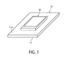
- FIG. 1 is a perspective view schematically showing an external shape of a power transmitting device and a power receiving device according to an embodiment.
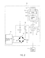
- FIG. 2 is a block diagram of the power transmitting device according to an embodiment.
- a power transmitting device includes a power supply unit, a power transmitting coil, a first switch, a piezoelectric element, and a first switch controller.
- a power receiving device can be placed on the power transmitting device.
- the power receiving device charges a built-in battery by using wirelessly received power.
- the power supply unit includes a power input terminal.
- the power supply unit is configured to generate a transmission power by using power supplied to the power input terminal.
- the power transmitting coil is configured to wirelessly transmit the transmission power to the power receiving device.
- the first switch electrically disconnects the external power supply and the power input terminal until the first switch is turned on next time by receiving the switch-on control.
- the piezoelectric element is disposed at a position at which a weight of the placed power receiving device can be detected.
- the piezoelectric element is configured to generate a detection power according to the weight of the placed power receiving device.
- the first switch controller is configured to generate a starting power by the detection power and switches the first switch to on by using the starting power.
- FIG. 1 is a perspective view schematically showing an external shape of a power transmitting device 10 and a power receiving device 20 according to an embodiment.
- the power transmitting device 10 includes a flat-plate-shaped housing 11 .
- the housing 11 includes an upper surface (a placing portion) 11 a on which the power receiving device 20 can be placed.
- the power receiving device 20 is placed on the upper surface 11 a of the housing 11 of the power transmitting device 10 .
- the power transmitting device 10 wirelessly transmits power to the power receiving device 20 from the side of the upper surface 11 a of the housing 11 by using electromagnetic induction.
- the power receiving device 20 includes a power receiving coil and a built-in battery.
- the power receiving device 20 charges the built-in battery by using power wirelessly received by the power receiving coil.
- the power receiving device 20 is a mobile device such as, for example, a mobile phone, a game console, and a camera and operates by power of a built-in battery. In this way, the power transmitting device 10 functions as a charging platform.
- the power transmitting device 10 transmits power and the power receiving device 20 receives power in compliance with, for example, a standard of Wireless Power Consortium (WPC).
- WPC Wireless Power Consortium
- FIG. 2 is a block diagram of the power transmitting device 10 according to an embodiment.
- the power transmitting device 10 includes a power supply unit 12 , a power transmitting coil 13 , a first switch SW 1 , a piezoelectric element (a piezo element) 14 , a first switch controller 15 , and a second switch controller 16 .
- the housing 11 shown in FIG. 1 houses the power supply unit 12 , the power transmitting coil 13 , the first switch SW 1 , the piezoelectric element 14 , the first switch controller 15 , and the second switch controller 16 .
- the power supply unit 12 includes a power input terminal 12 a and generates a transmission power by using AC power supplied to the power input terminal 12 a .
- the power supply unit 12 converts the supplied AC power into DC power and operates by the DC power.
- the power supply unit 12 includes a bridge circuit 121 such as a full bridge inverter for driving the power transmitting coil 13 and a control unit 122 for controlling the bridge circuit 121 and the power supply unit 12 in compliance with a standard of the Wireless Power Consortium.
- the power transmitting coil 13 is housed, for example, below the upper surface 11 a of the housing 11 and wirelessly transmits the transmission power generated by the power supply unit 12 to the power receiving device 20 .
- the first switch SW 1 is connected to an external power supply P and the other end thereof is connected to the power input terminal 12 a of the power supply unit 12 . Once the first switch SW 1 is turned on, the first switch SW 1 electrically connects the external power supply P and the power input terminal 12 a until the first switch SW 1 is turned off next time, and once the first switch SW 1 is turned off, the first switch SW 1 electrically disconnects the external power supply P and the power input terminal 12 a until the first switch SW 1 is turned on next time.
- the first switch SW 1 is, for example, a toggle switch or a mechanical relay.
- the external power supply P is a commercial AC power supply.
- the first switch SW 1 switches whether or not the AC power from the external power supply P is supplied to the power supply unit 12 . Normally, one end of the first switch SW 1 is connected to the external power supply P at all times using a power supply plug (not shown in FIG. 2 ).
- the piezoelectric element 14 is disposed at a position at which the weight of a placed power receiving device 20 can be detected, and generates a detection power Pd according to the weight of the placed power receiving device 20 .
- a columnar member is provided inside the upper surface 11 a of the housing 11 and the piezoelectric element 14 may be disposed at a position at which a pressure is applied by the columnar member when the power receiving device 20 is placed on the upper surface 11 a.
- the first switch controller 15 generates a starting power Pa by the detection power Pd and switches the first switch SW 1 to on by using the starting power Pa.
- the first switch controller 15 includes a bridge diode (a rectifier circuit) B 1 , a smoothing capacitor (a smoothing circuit) C 1 , a capacitor element (an electric power storage element) C 2 , and a second switch SW 2 .
- the bridge diode B 1 is a full-wave rectifier circuit including four diodes, which full wave rectifies the detection power Pd generated in the piezoelectric element 14 and outputs rectified power.
- the rectified power is supplied to one end of the smoothing capacitor C 1 and the ground is connected to the other end of the smoothing capacitor C 1 .
- the smoothing capacitor C 1 smoothes the rectified power.
- One end of the capacitor element C 2 is connected to the ground and a power that can switch the first switch SW 1 to on can be charged in the capacitor element C 2 .
- One end of the second switch SW 2 is connected to the other end of the capacitor element C 2 .
- the second switch SW 2 is turned on to output the power of the capacitor element C 2 from the other end thereof as the starting power Pa.
- the second switch SW 2 is turned off to stop the output of the starting power Pa.
- the second switch SW 2 is an N-type MOS transistor NM 1 which includes a source connected to the other end of the capacitor element C 2 , a gate to which a smoothed rectified power is supplied, and a drain that outputs the starting power Pa.
- the second switch controller 16 is provided on a side surface of the housing 11 so that a user can operate the second switch controller 16 .
- the second switch controller 16 switches the first switch SW 1 to on according to the operation of the user.
- the power supply unit 12 supplies a DC power to the other end of the capacitor element C 2 by using the AC power supplied to the power input terminal 12 a , so that the power supply unit 12 charges the capacitor element C 2 .
- the power receiving device 20 transmits a charge completion signal.
- the power supply unit 12 detects the charge completion signal through the power transmitting coil 13 , the power supply unit 12 switches the first switch SW 1 to off.
- the piezoelectric element 14 of the power transmitting device 10 does not generate the detection power Pd. Therefore, the N-type MOS transistor NM 1 is turned off. Also, the first switch SW 1 is turned off. Thereby, the AC power from the external power supply P is not consumed by the power transmitting device 10 , so that the standby power is zero.
- a weight (a pressure) is applied to the piezoelectric element 14 , so that the piezoelectric element 14 generates the detection power Pd.
- the N-type MOS transistor NM 1 is turned on to output the starting power Pa to the first switch SW 1 .
- the first switch SW 1 is turned on by the starting power Pa and the AC power from the external power supply P is supplied to the power supply unit 12 .
- the power supply unit 12 generates the transmission power and the power transmitting coil 13 transmits the transmission power to the power receiving device 20 .
- the piezoelectric element 14 generates the detection power Pd at an instant when the weight is applied to the piezoelectric element 14 and in a period of time in which the applied weight varies after that. Therefore, generally, it is assumed that the detection power Pd decreases to zero after the user has placed the power receiving device 20 and releases the power receiving device 20 from his or her hand.
- the first switch SW 1 which is a toggle switch or the like is turned on by receiving a switch-on control
- the first switch SW 1 electrically connects the external power supply P and the power input terminal 12 a until the first switch SW 1 is turned off by receiving a switch-off control independent from the switch-on control, so that the power transmitting device 10 can continuously transmit the transmission power.
- the power receiving device 20 charges the built-in battery by using the received power.
- the power receiving device 20 transmits a charge completion signal.
- the power supply unit 12 detects the charge completion signal through the power transmitting coil 13 , the power supply unit 12 switches the first switch SW 1 to off.
- the power transmitting device 10 becomes the standby state again, so that it is possible to eliminate the standby power.
- the power supply unit 12 charges the capacitor element C 2 by using the supplied AC power. Therefore, the first switch controller 15 can switch the first switch SW 1 to on by using the power charged in the capacitor element C 2 when the power receiving device 20 is placed next time.
- the first switch SW 1 cannot be switched to on if the standby state of the power transmitting device 10 continues for a long time and the capacitor element C 2 is discharged.
- the user may forcibly switch the first switch SW 1 to on by operating the second switch controller 16 .
- the power transmitting device 10 can recharge the capacitor element C 2 as well as transmit the transmission power.
- the power supply unit 12 may detect that the power receiving device 20 is not located nearby by, for example, a method in compliance with a standard of the Wireless Power Consortium, and thereby the power supply unit 12 may switch the first switch SW 1 to off. Thereby, the power transmitting device 10 becomes the standby state again.
- Examples of the methods for detecting the presence of the power receiving device 20 while charging the power receiving device 20 include various methods such as a method in which a PING signal is transmitted by the power supply unit 12 through the power transmitting coil 13 at a certain time interval and the presence or absence of a response from the power receiving device 20 is detected by the power supply unit 12 through the power transmitting coil 13 .
- the AC power from the external power supply P is prevented from being supplied to the power supply unit 12 by the first switch SW 1 which is in the off state.
- the piezoelectric element 14 When the power receiving device 20 is placed, the piezoelectric element 14 generates the detection power Pd, the first switch SW 1 is switched to on by using the detection power Pd, and the AC power from the external power supply P is supplied to the power supply unit 12 . In this way, the presence of the power receiving device 20 is detected by using the piezoelectric element 14 that does not require standby power, so that it is possible to eliminate the standby power of the power transmitting device 10 when the power receiving device 20 is not present nearby.
- the housing 11 of the power transmitting device 10 may have any shape if the housing 11 includes a placing portion on which the power receiving device 20 can be placed.
- the rectifier circuit is a full-wave rectifier circuit (the bridge diode B 1 ), for example, the rectifier circuit may be a half-wave rectifier circuit.
- the electric power storage element is the capacitor element C 2
- the electric power storage element may be a storage battery. If the storage battery can hold power even when the standby state of the power transmitting device 10 continues for a long time, the second switch controller 16 need not be provided.
- the external power supply P is an AC power supply
- the external power supply P may be a DC power supply.
- the power supply unit 12 operates by supplied DC power.
- An AC adaptor may be included between the external power supply P which is an AC power supply and one end of the first switch SW 1 of the power transmitting device 10 . Also in this case, in the same manner as in the above embodiment, it is possible to eliminate the standby power of the power transmitting device 10 in the standby state. However, there is the standby power of the AC adaptor itself.
- the power transmitting device 10 and the power receiving device 20 need not be in compliance with a standard of the Wireless Power Consortium.
Landscapes
- Engineering & Computer Science (AREA)
- Power Engineering (AREA)
- Computer Networks & Wireless Communication (AREA)
- Charge And Discharge Circuits For Batteries Or The Like (AREA)
- Secondary Cells (AREA)
Abstract
Description
Claims (17)
Applications Claiming Priority (2)
| Application Number | Priority Date | Filing Date | Title |
|---|---|---|---|
| JP2012117653A JP5814858B2 (en) | 2012-05-23 | 2012-05-23 | Power transmission equipment |
| JP2012-117653 | 2012-05-23 |
Publications (2)
| Publication Number | Publication Date |
|---|---|
| US20130313910A1 US20130313910A1 (en) | 2013-11-28 |
| US8648564B2 true US8648564B2 (en) | 2014-02-11 |
Family
ID=49621037
Family Applications (1)
| Application Number | Title | Priority Date | Filing Date |
|---|---|---|---|
| US13/608,033 Expired - Fee Related US8648564B2 (en) | 2012-05-23 | 2012-09-10 | Power transmitting device |
Country Status (2)
| Country | Link |
|---|---|
| US (1) | US8648564B2 (en) |
| JP (1) | JP5814858B2 (en) |
Families Citing this family (8)
| Publication number | Priority date | Publication date | Assignee | Title |
|---|---|---|---|---|
| JP2013070520A (en) * | 2011-09-22 | 2013-04-18 | Panasonic Corp | Driving method of non contact power supply device, non contact power supply device, and non contact power supply system |
| KR20210096686A (en) * | 2012-11-05 | 2021-08-05 | 애플 인크. | Inductively coupled power transfer systems |
| US9385787B2 (en) * | 2014-01-29 | 2016-07-05 | Nokia Technologies Oy | Communications via wireless charging |
| GB2526126A (en) * | 2014-05-14 | 2015-11-18 | Bombardier Transp Gmbh | Inductive power transfer arrangement with object detection |
| KR20160025314A (en) | 2014-08-27 | 2016-03-08 | 현대자동차주식회사 | Wireless charging system for variable charging mode |
| US10013025B2 (en) * | 2014-12-11 | 2018-07-03 | Intel Corporation | Wearable device with power state control |
| US20160182043A1 (en) * | 2014-12-23 | 2016-06-23 | Sivapathalingham Sivavakeesar | Context-Aware Electronic Apparatus, System and Methods thereof |
| EP3125065B1 (en) * | 2015-07-31 | 2018-12-19 | Power Integrations Switzerland GmbH | Communicating across galvanic isolation |
Citations (10)
| Publication number | Priority date | Publication date | Assignee | Title |
|---|---|---|---|---|
| JP2002078360A (en) | 2000-08-25 | 2002-03-15 | National Institute Of Advanced Industrial & Technology | Cableless power supply method |
| JP2002084688A (en) | 2000-09-07 | 2002-03-22 | Furukawa Electric Co Ltd:The | Separation type power supply method and device |
| JP2002142388A (en) | 1998-12-22 | 2002-05-17 | Seiko Epson Corp | Power feeder |
| US20040260470A1 (en) * | 2003-06-14 | 2004-12-23 | Rast Rodger H. | Conveyance scheduling and logistics system |
| US7279807B2 (en) * | 2002-09-27 | 2007-10-09 | Honda Giken Kogyo Kabushiki Kaisha | Vehicle electronic key system |
| US7710288B2 (en) * | 2006-02-09 | 2010-05-04 | Alps Automotive, Inc. | Wireless self-powered sensor |
| US20100231163A1 (en) * | 2007-09-26 | 2010-09-16 | Governing Dynamics, Llc | Self-Charging Electric Vehicles and Aircraft, and Wireless Energy Distribution System |
| JP2011083067A (en) | 2009-10-02 | 2011-04-21 | Nec Casio Mobile Communications Ltd | Non-contact charging apparatus and terminal device therefor, and program |
| US20110115303A1 (en) * | 2009-11-19 | 2011-05-19 | Access Business Group International Llc | Multiple use wireless power systems |
| US20120112543A1 (en) * | 2009-07-13 | 2012-05-10 | Koninklijke Philips Electronics N.V. | Inductive power transfer |
Family Cites Families (6)
| Publication number | Priority date | Publication date | Assignee | Title |
|---|---|---|---|---|
| JP2003209934A (en) * | 2002-01-10 | 2003-07-25 | Alps Electric Co Ltd | Charging system for portable device |
| WO2007127106A2 (en) * | 2006-04-28 | 2007-11-08 | Cooper Tire & Rubber Company | Long range rfid transponder |
| JP5556002B2 (en) * | 2008-01-09 | 2014-07-23 | セイコーエプソン株式会社 | Power transmission control device, power transmission device, non-contact power transmission system, and electronic device |
| US8125122B2 (en) * | 2009-07-02 | 2012-02-28 | Sony Ericsson Mobile Communications Ab | Method and circuit for energizing an electrical device |
| EP2317626B1 (en) * | 2009-10-27 | 2017-12-20 | BlackBerry Limited | Holster-integrated piezoelectric energy source for handheld electronic device |
| US20130062960A1 (en) * | 2009-12-04 | 2013-03-14 | Powermat Technologies Ltd. | System and method for controlling the connection from a power supply to an inductive power outlet |
-
2012
- 2012-05-23 JP JP2012117653A patent/JP5814858B2/en not_active Expired - Fee Related
- 2012-09-10 US US13/608,033 patent/US8648564B2/en not_active Expired - Fee Related
Patent Citations (11)
| Publication number | Priority date | Publication date | Assignee | Title |
|---|---|---|---|---|
| JP2002142388A (en) | 1998-12-22 | 2002-05-17 | Seiko Epson Corp | Power feeder |
| JP2002078360A (en) | 2000-08-25 | 2002-03-15 | National Institute Of Advanced Industrial & Technology | Cableless power supply method |
| US6635818B2 (en) | 2000-08-25 | 2003-10-21 | National Institute Of Advanced Industrial Science And Technology | Wireless power supply method |
| JP2002084688A (en) | 2000-09-07 | 2002-03-22 | Furukawa Electric Co Ltd:The | Separation type power supply method and device |
| US7279807B2 (en) * | 2002-09-27 | 2007-10-09 | Honda Giken Kogyo Kabushiki Kaisha | Vehicle electronic key system |
| US20040260470A1 (en) * | 2003-06-14 | 2004-12-23 | Rast Rodger H. | Conveyance scheduling and logistics system |
| US7710288B2 (en) * | 2006-02-09 | 2010-05-04 | Alps Automotive, Inc. | Wireless self-powered sensor |
| US20100231163A1 (en) * | 2007-09-26 | 2010-09-16 | Governing Dynamics, Llc | Self-Charging Electric Vehicles and Aircraft, and Wireless Energy Distribution System |
| US20120112543A1 (en) * | 2009-07-13 | 2012-05-10 | Koninklijke Philips Electronics N.V. | Inductive power transfer |
| JP2011083067A (en) | 2009-10-02 | 2011-04-21 | Nec Casio Mobile Communications Ltd | Non-contact charging apparatus and terminal device therefor, and program |
| US20110115303A1 (en) * | 2009-11-19 | 2011-05-19 | Access Business Group International Llc | Multiple use wireless power systems |
Also Published As
| Publication number | Publication date |
|---|---|
| JP2013247707A (en) | 2013-12-09 |
| US20130313910A1 (en) | 2013-11-28 |
| JP5814858B2 (en) | 2015-11-17 |
Similar Documents
| Publication | Publication Date | Title |
|---|---|---|
| US8648564B2 (en) | Power transmitting device | |
| JP7026646B2 (en) | A wireless power transmission control method in a resonance type wireless power transmission system, a wireless power transmission device using the same, and a wireless power receiving device using the same. | |
| KR102584438B1 (en) | Device for adjusting path of power and operation method thereof | |
| US8188709B2 (en) | Power transmission control device, power transmitting device, non-contact power transmitting system, and electronic instrument | |
| US9130380B2 (en) | Contactless power transmitting system having overheat protection function and method thereof | |
| KR101243587B1 (en) | Non-contract charging device, non-contact charghing system and non-contact charging method | |
| US9142999B2 (en) | Systems, methods, and apparatus for small device wireless charging modes | |
| JP6498391B2 (en) | Mobile device and control method thereof | |
| US20150333530A1 (en) | Operating a Wireless Power Transfer System at Multiple Frequencies | |
| US20110260681A1 (en) | Portable Wireless Charging Device | |
| US9900056B2 (en) | System and method for delayed application processor initialization during wireless charging | |
| US9997927B2 (en) | Power transmission apparatus, control method of power transmission apparatus, and storage medium | |
| JP2009504117A (en) | Charging power supply device, battery device, contactless charging system, and charging method | |
| US20120326661A1 (en) | Contactless power receiving device, and contactless charging system | |
| US20160126747A1 (en) | Non-contact power transmission apparatus and power transmission device | |
| US20140266020A1 (en) | Wireless charging pad and method | |
| US9531213B2 (en) | Wireless power transmission device | |
| KR101063156B1 (en) | Solid state charging control device and charging control method | |
| US20160028269A1 (en) | System for wireless exchange of power between mobile devices | |
| JP2016059115A (en) | Non-contact power transmission device | |
| CN105340154B (en) | Electrical power transmission system | |
| JP2014217116A (en) | Electronic apparatus, electronic apparatus power transmission system and power reception control method | |
| JP2025121885A (en) | Techniques for wireless charging negotiation | |
| KR102698751B1 (en) | Wireless power transmitting device and method | |
| KR101505650B1 (en) | wireless energy and data transmission system using light for mobile phone |
Legal Events
| Date | Code | Title | Description |
|---|---|---|---|
| AS | Assignment |
Owner name: KABUSHIKI KAISHA TOSHIBA, JAPAN Free format text: ASSIGNMENT OF ASSIGNORS INTEREST;ASSIGNOR:SASAKI, KENICHI;REEL/FRAME:028926/0369 Effective date: 20120903 |
|
| FEPP | Fee payment procedure |
Free format text: PAYOR NUMBER ASSIGNED (ORIGINAL EVENT CODE: ASPN); ENTITY STATUS OF PATENT OWNER: LARGE ENTITY |
|
| STCF | Information on status: patent grant |
Free format text: PATENTED CASE |
|
| FEPP | Fee payment procedure |
Free format text: PAYOR NUMBER ASSIGNED (ORIGINAL EVENT CODE: ASPN); ENTITY STATUS OF PATENT OWNER: LARGE ENTITY Free format text: PAYER NUMBER DE-ASSIGNED (ORIGINAL EVENT CODE: RMPN); ENTITY STATUS OF PATENT OWNER: LARGE ENTITY |
|
| FPAY | Fee payment |
Year of fee payment: 4 |
|
| FEPP | Fee payment procedure |
Free format text: MAINTENANCE FEE REMINDER MAILED (ORIGINAL EVENT CODE: REM.); ENTITY STATUS OF PATENT OWNER: LARGE ENTITY |
|
| LAPS | Lapse for failure to pay maintenance fees |
Free format text: PATENT EXPIRED FOR FAILURE TO PAY MAINTENANCE FEES (ORIGINAL EVENT CODE: EXP.); ENTITY STATUS OF PATENT OWNER: LARGE ENTITY |
|
| STCH | Information on status: patent discontinuation |
Free format text: PATENT EXPIRED DUE TO NONPAYMENT OF MAINTENANCE FEES UNDER 37 CFR 1.362 |
|
| FP | Lapsed due to failure to pay maintenance fee |
Effective date: 20220211 |