US8647519B1 - Manufacturing method of touchpad - Google Patents
Manufacturing method of touchpad Download PDFInfo
- Publication number
- US8647519B1 US8647519B1 US13/760,054 US201313760054A US8647519B1 US 8647519 B1 US8647519 B1 US 8647519B1 US 201313760054 A US201313760054 A US 201313760054A US 8647519 B1 US8647519 B1 US 8647519B1
- Authority
- US
- United States
- Prior art keywords
- layer
- touch
- manufacturing
- touchpad
- substrate
- Prior art date
- Legal status (The legal status is an assumption and is not a legal conclusion. Google has not performed a legal analysis and makes no representation as to the accuracy of the status listed.)
- Expired - Fee Related
Links
Images


Classifications
-
- G—PHYSICS
- G06—COMPUTING OR CALCULATING; COUNTING
- G06F—ELECTRIC DIGITAL DATA PROCESSING
- G06F3/00—Input arrangements for transferring data to be processed into a form capable of being handled by the computer; Output arrangements for transferring data from processing unit to output unit, e.g. interface arrangements
- G06F3/01—Input arrangements or combined input and output arrangements for interaction between user and computer
- G06F3/03—Arrangements for converting the position or the displacement of a member into a coded form
- G06F3/041—Digitisers, e.g. for touch screens or touch pads, characterised by the transducing means
- G06F3/0412—Digitisers structurally integrated in a display
-
- G—PHYSICS
- G06—COMPUTING OR CALCULATING; COUNTING
- G06F—ELECTRIC DIGITAL DATA PROCESSING
- G06F3/00—Input arrangements for transferring data to be processed into a form capable of being handled by the computer; Output arrangements for transferring data from processing unit to output unit, e.g. interface arrangements
- G06F3/01—Input arrangements or combined input and output arrangements for interaction between user and computer
- G06F3/03—Arrangements for converting the position or the displacement of a member into a coded form
- G06F3/041—Digitisers, e.g. for touch screens or touch pads, characterised by the transducing means
- G06F3/044—Digitisers, e.g. for touch screens or touch pads, characterised by the transducing means by capacitive means
- G06F3/0443—Digitisers, e.g. for touch screens or touch pads, characterised by the transducing means by capacitive means using a single layer of sensing electrodes
-
- G—PHYSICS
- G06—COMPUTING OR CALCULATING; COUNTING
- G06F—ELECTRIC DIGITAL DATA PROCESSING
- G06F2203/00—Indexing scheme relating to G06F3/00 - G06F3/048
- G06F2203/041—Indexing scheme relating to G06F3/041 - G06F3/045
- G06F2203/04103—Manufacturing, i.e. details related to manufacturing processes specially suited for touch sensitive devices
Definitions
- the present invention relates generally to a manufacturing method of touchpad, and more particularly to a manufacturing method of touchpad, which can save the cost for the masks to lower the manufacturing cost.
- the display screen of a digital product such as mobile phone, PDA, notebook and tablet is an inevitable human/device communication interface.
- the display screen facilitates operation of the digital product.
- the display screen is a liquid crystal display as a mainstream.
- the touch liquid crystal display device is shortened to touch panel hereinafter.
- the touch panel is laminated structure including glass substrate, touch electrode layer, shield layer, electrode wiring layer, insulation layer and protection layer. These layers are stacked to form the laminated structure.
- the glass substrate has a touch section and a non-touch section.
- the touch electrode layer is coated on rear side of the touch section of the glass substrate by means of sputtering. Then the touch electrodes are formed by means of lithography and etching processes. Then an ink layer is printed on the non-touch section of the substrate as the shield layer.
- the electrode wiring layer is coated on the shield layer by means of sputtering. Then the electrode wires are formed by means of lithography and etching processes.
- the protection layer is coated on the glass substrate, the touch electrode layer, the shield layer, the electrode wiring layer and the insulation layer by means of coating.
- the touch electrodes and the electrode wires are formed by means of sputtering, lithography and etching processes.
- the cost for the mask is quite high and the sputtering process is quite time-consuming.
- the manufacturing cost of the conventional touch panel is very high and the manufacturing time of the conventional touch panel is relatively long.
- the manufacturing method of touchpad of the present invention includes steps of:
- the manufacturing time is greatly shortened and the use of the mask is reduced so that the manufacturing cost is lowered.
- FIG. 1 is a flow chart of a first embodiment of the manufacturing method of touchpad of the present invention
- FIG. 2 is a schematic diagram showing the structure of the touchpad of the first embodiment of the manufacturing method of touchpad of the present invention
- FIG. 3 is a schematic diagram showing the first embodiment of the manufacturing method of touchpad of the present invention.
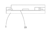
- FIG. 4 is a flow chart of a second embodiment of the manufacturing method of touchpad of the present invention.
- FIG. 5 is a schematic diagram showing the structure of the touchpad of the second embodiment of the manufacturing method of touchpad of the present invention.
- FIG. 1 is a flow chart of a first embodiment of the manufacturing method of touchpad of the present invention.
- FIG. 2 is a schematic diagram showing the structure of the touchpad of the first embodiment of the manufacturing method of touchpad of the present invention.
- FIG. 3 is a schematic diagram showing the first embodiment of the manufacturing method of touchpad of the present invention.
- the manufacturing method of touchpad of the present invention includes steps of:
- S 1 providing a substrate and disposing a shield layer on the substrate, a section of the substrate, where the shield layer is positioned being defined as a non-touch section, a section of the substrate, which is free from the shield layer being defined as a touch section, a substrate 1 being provided, the substrate 1 being a transparent board material made of glass or polymer material, an ink being sprayed onto the substrate 1 to form a shield layer 11 thereon, a section of the substrate 1 , where the shield layer 11 is positioned being defined as a non-touch section 12 , while a section of the substrate 1 , which is free from the shield layer 11 being defined as a touch section 13 , in this embodiment, the substrate 1 being made of transparent glass material by means of a process, which is identical to that of the conventional manufacturing method and thus will not be further described hereinafter; S 2 .
- a touch electrode layer with multiple touch electrodes on the substrate a touch electrode layer 14 being formed on the substrate 1 by means of sputtering, the touch electrode layer 14 being selected from a group consisting of indium tin oxide (ITO), indium zinc oxide, indium tin zinc oxide, hafnium oxide, zinc oxide, aluminum oxide, aluminum tin oxide, aluminum zinc oxide, cadmium tin oxide and cadmium zinc oxide;
- ITO indium tin oxide
- ITO indium zinc oxide
- indium tin zinc oxide hafnium oxide
- zinc oxide aluminum oxide
- aluminum tin oxide aluminum zinc oxide
- S 3 disposing a metal wiring layer with multiple metal wires on the touch electrode layer, a metal wiring layer 15 being disposed on the touch electrode layer 14 by means of sputtering
- S 4 disposing a touch electrode layer with multiple touch electrodes on the substrate, a touch electrode layer 14 being formed on the substrate 1 by means of
- the etching liquid used in the first time of lithography and etching processes being selected from a group consisting of phosphate, nitric acid, acetic acid and water; S 5 .
- the etching liquid used in the second time of lithography and etching processes being selected from a group consisting of nitric acid, hydrochloric acid and water; S 6 .
- the insulation layer 16 being formed with multiple electrical connection holes corresponding to the touch electrodes, an insulation layer 16 being coated on the junctions between the touch electrodes and the metal wires in the non-touch section 12 , a wet etching process being performed to the insulation layer 16 to form multiple electrical connection holes 161 corresponding to the touch electrodes 141 , the insulation layer 16 being formed by means of halftone print process or plate print process, the insulation layer 16 being made of a material with a dielectric coefficient of 2-4, which can be a transparent insulation material such as ink or a nontransparent insulation material or an inorganic material or an organic material, the inorganic material being selected from a group consisting of silicon oxide, silicon nitride, silicon oxynitride, silicon carbide, hafnium oxide and aluminum oxide, the organic material being selected from a group consisting of photoresistor, enzocyclobutane (BCB), cycloolefins, polyesters, polyalcohols, poly
- a lead layer with multiple metal leads on the insulation layer disposing a lead layer with multiple metal leads on the insulation layer, the metal leads passing through the electrical connection holes to electrically connect with the touch electrodes, metal leads 17 being disposed on the insulation layer 16 and in the preformed electrical connection holes 161 by means of silver paste printing or sputtering so as to electrically connect the touch electrodes 141 to the metal wires 151 ; and S 8 .
- disposing a protection layer on the touch electrode layer and the lead layer and the insulation layer a protection layer 18 being formed on the touch electrode layer 141 , the metal wiring layer 151 and the insulation layer 16 by means of deposition so as to protect the touch electrode layer 141 , the insulation layer 16 and the metal leads 17 .
- FIG. 4 is a flow chart of a second embodiment of the manufacturing method of touchpad of the present invention.
- FIG. 5 is a schematic diagram showing the structure of the touchpad of the second embodiment of the manufacturing method of touchpad of the present invention.
- the manufacturing method of touchpad of the present invention includes steps of:
- S 1 providing a substrate and disposing a shield layer on the substrate, a section of the substrate, where the shield layer is positioned being defined as a non-touch section, a section of the substrate, which is free from the shield layer being defined as a touch section;
- S 2 disposing a touch electrode layer with multiple touch electrodes on the substrate;
- S 3 disposing a metal wiring layer with multiple metal wires on the touch electrode layer;
- S 4 performing a first time of lithography and etching processes to the metal wiring layer so as to form multiple metal wires on the non-touch section;
- S 5 performing a second time of lithography and etching processes to the touch electrode layer so as to form multiple touch electrodes on the non-touch section and the touch section;
- S 6 performs a first time of lithography and etching processes to the metal wiring layer so as to form multiple touch electrodes on the non-touch section and the touch section;
- the second embodiment is partially identical to the first embodiment and thus will not be further described hereinafter.
- the second embodiment is different from the first embodiment in that between step S 2 of disposing a touch electrode layer with multiple touch electrodes on the substrate and step S 3 of disposing a metal wiring layer with multiple metal wires on the touch electrode layer, the second embodiment further includes a step S 2 - 1 of forming an optical compensation layer on the touch section and the non-touch section.
- the optical compensation layer 19 is disposed on the substrate by means of sputtering.
- the manufacturing time is greatly shortened and the use of the mask is reduced so that the manufacturing cost is lowered.
- the present invention has the following advantages:
Landscapes
- Engineering & Computer Science (AREA)
- General Engineering & Computer Science (AREA)
- Theoretical Computer Science (AREA)
- Human Computer Interaction (AREA)
- Physics & Mathematics (AREA)
- General Physics & Mathematics (AREA)
- Position Input By Displaying (AREA)
- Manufacture Of Switches (AREA)
Abstract
Description
disposing a touch electrode layer with multiple touch electrodes on the substrate;
disposing a metal wiring layer with multiple metal wires on the touch electrode layer;
performing a first time of lithography and etching processes to the metal wiring layer so as to form multiple metal wires on the non-touch section;
performing a second time of lithography and etching processes to the touch electrode layer so as to form multiple touch electrodes on the non-touch section and the touch section;
disposing an insulation layer on the touch electrodes, the insulation layer being formed with multiple electrical connection holes corresponding to the touch electrodes;
disposing a lead layer with multiple metal leads on the insulation layer, the metal leads passing through the electrical connection holes to electrically connect with the touch electrodes; and
disposing a protection layer on the touch electrode layer and the lead layer and the insulation layer.
S2. disposing a touch electrode layer with multiple touch electrodes on the substrate, a
S3. disposing a metal wiring layer with multiple metal wires on the touch electrode layer, a
S4. performing a first time of lithography and etching processes to the metal wiring layer so as to form multiple metal wires on the non-touch section, a first time of lithography and etching processes being performed to the
S5. performing a second time of lithography and etching processes to the touch electrode layer so as to form multiple touch electrodes on the non-touch section and the touch section, a second time of lithography and etching processes being performed to the
S6. disposing an insulation layer on the touch electrodes, the insulation layer being formed with multiple electrical connection holes corresponding to the touch electrodes, an
S7. disposing a lead layer with multiple metal leads on the insulation layer, the metal leads passing through the electrical connection holes to electrically connect with the touch electrodes, metal leads 17 being disposed on the
S8. disposing a protection layer on the touch electrode layer and the lead layer and the insulation layer, a
S2. disposing a touch electrode layer with multiple touch electrodes on the substrate;
S3. disposing a metal wiring layer with multiple metal wires on the touch electrode layer;
S4. performing a first time of lithography and etching processes to the metal wiring layer so as to form multiple metal wires on the non-touch section;
S5. performing a second time of lithography and etching processes to the touch electrode layer so as to form multiple touch electrodes on the non-touch section and the touch section;
S6. disposing an insulation layer on the touch electrodes, the insulation layer being formed with multiple electrical connection holes corresponding to the touch electrodes;
S7. disposing a lead layer with multiple metal leads on the insulation layer, the metal leads passing through the electrical connection holes to electrically connect with the touch electrodes; and
S8. disposing a protection layer on the touch electrode layer and the lead layer and the insulation layer.
Claims (10)
Applications Claiming Priority (2)
| Application Number | Priority Date | Filing Date | Title |
|---|---|---|---|
| TW101148209A TWI436252B (en) | 2012-12-19 | 2012-12-19 | Manufacturing method of touchpad |
| TW101148209A | 2012-12-19 |
Publications (1)
| Publication Number | Publication Date |
|---|---|
| US8647519B1 true US8647519B1 (en) | 2014-02-11 |
Family
ID=50032725
Family Applications (1)
| Application Number | Title | Priority Date | Filing Date |
|---|---|---|---|
| US13/760,054 Expired - Fee Related US8647519B1 (en) | 2012-12-19 | 2013-02-06 | Manufacturing method of touchpad |
Country Status (2)
| Country | Link |
|---|---|
| US (1) | US8647519B1 (en) |
| TW (1) | TWI436252B (en) |
Cited By (8)
| Publication number | Priority date | Publication date | Assignee | Title |
|---|---|---|---|---|
| US20140165383A1 (en) * | 2012-12-19 | 2014-06-19 | Chih-Chung Lin | Manufacturing method of touch panel |
| US20140335785A1 (en) * | 2012-12-21 | 2014-11-13 | Murata Manufacturing Co., Ltd. | Interface unit and computer |
| CN105573533A (en) * | 2014-10-09 | 2016-05-11 | 宸鸿科技(厦门)有限公司 | Touch control panel |
| US20170090607A1 (en) * | 2015-09-24 | 2017-03-30 | Boe Technology Group Co., Ltd. | One-glass-solution touch panel, its manufacturing method and display device |
| WO2017105530A1 (en) * | 2015-12-16 | 2017-06-22 | 3M Innovative Properties Company | Transparent conductive component with interconnect circuit tab comprising cured organic polymeric material |
| CN107759106A (en) * | 2017-09-27 | 2018-03-06 | 广东星弛光电科技有限公司 | A kind of manufacture method of mobile phone capacitive touch screen cover-plate glass |
| US11366541B2 (en) * | 2020-10-30 | 2022-06-21 | Wuhan Tianma Micro-Electronics Co., Ltd. | Display device and electronic apparatus |
| US12482917B2 (en) | 2021-09-16 | 2025-11-25 | Samsung Electronics Co., Ltd. | Electronic device comprising antenna |
Families Citing this family (2)
| Publication number | Priority date | Publication date | Assignee | Title |
|---|---|---|---|---|
| CN104951151A (en) * | 2014-03-27 | 2015-09-30 | 林志忠 | Touch module manufacturing method |
| TWI512572B (en) * | 2014-03-27 | 2015-12-11 | Chih Chung Lin | Manufacturing method of touch module |
Citations (1)
| Publication number | Priority date | Publication date | Assignee | Title |
|---|---|---|---|---|
| US20100026661A1 (en) * | 2008-07-31 | 2010-02-04 | Hitachi Displays, Ltd. | Display Device |
-
2012
- 2012-12-19 TW TW101148209A patent/TWI436252B/en not_active IP Right Cessation
-
2013
- 2013-02-06 US US13/760,054 patent/US8647519B1/en not_active Expired - Fee Related
Patent Citations (1)
| Publication number | Priority date | Publication date | Assignee | Title |
|---|---|---|---|---|
| US20100026661A1 (en) * | 2008-07-31 | 2010-02-04 | Hitachi Displays, Ltd. | Display Device |
Cited By (14)
| Publication number | Priority date | Publication date | Assignee | Title |
|---|---|---|---|---|
| US9153393B2 (en) * | 2012-12-19 | 2015-10-06 | Chih-Chung Lin | Manufacturing method of touch panel |
| US20140165383A1 (en) * | 2012-12-19 | 2014-06-19 | Chih-Chung Lin | Manufacturing method of touch panel |
| US20170133743A1 (en) * | 2012-12-21 | 2017-05-11 | Murata Manufacturing Co., Ltd. | Interface unit and computer |
| US20140335785A1 (en) * | 2012-12-21 | 2014-11-13 | Murata Manufacturing Co., Ltd. | Interface unit and computer |
| US9590700B2 (en) * | 2012-12-21 | 2017-03-07 | Murata Manufacturing Co., Ltd. | Interface unit and computer |
| US10581139B2 (en) * | 2012-12-21 | 2020-03-03 | Murata Manufacturing Co., Ltd. | Interface unit and computer |
| CN105573533A (en) * | 2014-10-09 | 2016-05-11 | 宸鸿科技(厦门)有限公司 | Touch control panel |
| CN105573533B (en) * | 2014-10-09 | 2021-03-16 | 宸鸿科技(厦门)有限公司 | touch panel |
| US20170090607A1 (en) * | 2015-09-24 | 2017-03-30 | Boe Technology Group Co., Ltd. | One-glass-solution touch panel, its manufacturing method and display device |
| WO2017105530A1 (en) * | 2015-12-16 | 2017-06-22 | 3M Innovative Properties Company | Transparent conductive component with interconnect circuit tab comprising cured organic polymeric material |
| US9857930B2 (en) | 2015-12-16 | 2018-01-02 | 3M Innovative Properties Company | Transparent conductive component with interconnect circuit tab comprising cured organic polymeric material |
| CN107759106A (en) * | 2017-09-27 | 2018-03-06 | 广东星弛光电科技有限公司 | A kind of manufacture method of mobile phone capacitive touch screen cover-plate glass |
| US11366541B2 (en) * | 2020-10-30 | 2022-06-21 | Wuhan Tianma Micro-Electronics Co., Ltd. | Display device and electronic apparatus |
| US12482917B2 (en) | 2021-09-16 | 2025-11-25 | Samsung Electronics Co., Ltd. | Electronic device comprising antenna |
Also Published As
| Publication number | Publication date |
|---|---|
| TW201403413A (en) | 2014-01-16 |
| TWI436252B (en) | 2014-05-01 |
Similar Documents
| Publication | Publication Date | Title |
|---|---|---|
| US8647519B1 (en) | Manufacturing method of touchpad | |
| CN107512050B (en) | Touch panel, manufacturing method thereof, and touch display device | |
| TW201349049A (en) | Touch panel and manufacturing method thereof | |
| CN107025027A (en) | Touch base plate and preparation method thereof, display panel and display device | |
| TWI553711B (en) | Touch panel and method for manufacturing the same | |
| US20180239471A1 (en) | Touch-sensor structures and methods of forming the same | |
| US9274634B2 (en) | Touch panel | |
| TW201606594A (en) | Conductive structure body and method for manufacturing the same, and display device | |
| US9600105B2 (en) | Touch panel device and method for manufacturing the same | |
| US9304645B2 (en) | Manufacturing method of touch module | |
| CN103092379A (en) | Image display system and method for manufacturing touch sensing device | |
| CN103885621B (en) | Touch panel manufacturing method | |
| CN101776815B (en) | Touch display panel and manufacture method thereof | |
| US9153393B2 (en) | Manufacturing method of touch panel | |
| CN109375829A (en) | A manufacturing method of a display device using a metal mesh double touch sensor | |
| CN104182067A (en) | Touch panel and manufacturing method thereof | |
| CN104345927B (en) | Touch device manufacturing method | |
| CN104951151A (en) | Touch module manufacturing method | |
| CN103885619B (en) | touch panel manufacturing method | |
| JP5588525B2 (en) | Manufacturing method of touch panel | |
| KR20150019058A (en) | Touch screen panel and manufacturing method thereof | |
| TWI512572B (en) | Manufacturing method of touch module | |
| JP5750126B2 (en) | Touch control panel manufacturing method | |
| CN204028871U (en) | touch module | |
| US20150053639A1 (en) | Method of manufacturing touch devices |
Legal Events
| Date | Code | Title | Description |
|---|---|---|---|
| STCF | Information on status: patent grant |
Free format text: PATENTED CASE |
|
| FPAY | Fee payment |
Year of fee payment: 4 |
|
| MAFP | Maintenance fee payment |
Free format text: PAYMENT OF MAINTENANCE FEE, 8TH YR, SMALL ENTITY (ORIGINAL EVENT CODE: M2552); ENTITY STATUS OF PATENT OWNER: SMALL ENTITY Year of fee payment: 8 |
|
| FEPP | Fee payment procedure |
Free format text: MAINTENANCE FEE REMINDER MAILED (ORIGINAL EVENT CODE: REM.); ENTITY STATUS OF PATENT OWNER: SMALL ENTITY |
|
| LAPS | Lapse for failure to pay maintenance fees |
Free format text: PATENT EXPIRED FOR FAILURE TO PAY MAINTENANCE FEES (ORIGINAL EVENT CODE: EXP.); ENTITY STATUS OF PATENT OWNER: SMALL ENTITY |
|
| STCH | Information on status: patent discontinuation |
Free format text: PATENT EXPIRED DUE TO NONPAYMENT OF MAINTENANCE FEES UNDER 37 CFR 1.362 |
|
| FP | Lapsed due to failure to pay maintenance fee |
Effective date: 20260211 |