US8643446B2 - Electro-magnetic interference reduction using opposing field transmitter - Google Patents
Electro-magnetic interference reduction using opposing field transmitter Download PDFInfo
- Publication number
- US8643446B2 US8643446B2 US13/020,443 US201113020443A US8643446B2 US 8643446 B2 US8643446 B2 US 8643446B2 US 201113020443 A US201113020443 A US 201113020443A US 8643446 B2 US8643446 B2 US 8643446B2
- Authority
- US
- United States
- Prior art keywords
- signal
- antenna
- circuit
- accordance
- operational
- Prior art date
- Legal status (The legal status is an assumption and is not a legal conclusion. Google has not performed a legal analysis and makes no representation as to the accuracy of the status listed.)
- Active, expires
Links
Images


Classifications
-
- H—ELECTRICITY
- H04—ELECTRIC COMMUNICATION TECHNIQUE
- H04B—TRANSMISSION
- H04B15/00—Suppression or limitation of noise or interference
- H04B15/02—Reducing interference from electric apparatus by means located at or near the interfering apparatus
-
- H—ELECTRICITY
- H04—ELECTRIC COMMUNICATION TECHNIQUE
- H04B—TRANSMISSION
- H04B1/00—Details of transmission systems, not covered by a single one of groups H04B3/00 - H04B13/00; Details of transmission systems not characterised by the medium used for transmission
- H04B1/06—Receivers
- H04B1/10—Means associated with receiver for limiting or suppressing noise or interference
- H04B1/12—Neutralising, balancing, or compensation arrangements
Definitions
- EMC electromagnetic compatibility
- EMI Electro-Magnetic Interference
- EMI will radiate to some extent every time a time-dependent voltage or current signal is present on chip. If the EMI is excessive, the functionality of the circuit or its surrounding circuitry may be adversely affected. Also, there are sometimes strict you limits to the amount of EMI that may be emitted as a function of frequency. For instance, in the United States, the Federal Communication Commission (FCC) regulates the usage of certain frequencies of electromagnetic energy.
- FCC Federal Communication Commission
- Passive filtering removes higher frequency harmonics from a signal, thereby degrading signal integrity. Passive components cannot be used to reduce the EMI in the fundamental frequency of a signal unless they reduce the signal amplitude, which is also a trade-off between signal quality and EMI reduction. Spread spectrum generation is an effective solution but there are instances where the deviation in frequency cannot exceed a certain limit and hence spread spectrum generation is typically a trade-off between EMI reduction and functionality of the system. In shielding, the signal is shielded using a metal and dielectric case or layers to contain the electromagnetic waves within a certain physical zone.
- At least one embodiment described herein relates to an electronic system that includes or is proximate a functional circuit that carries an operational signal.
- An unwanted side effect of the operational signal is that the functional circuit can act as a transmission antenna causing unwanted emissions of electromagnetic interference (EMI).
- EMI electromagnetic interference
- An antenna signal generation circuit is coupled to the antenna circuit and generates the antenna signal.
- the antenna signal has the characteristic such that when the antenna signal is applied to the antenna circuit, the resultant emitted electromagnetic radiation at least partially offsets electromagnetic interference emitted by the operational signal from the functional circuit.
- the generation of the antenna signal is performed without reducing the signal quality of the operational signal.
- FIG. 1 illustrates an electrical circuit that includes a functional circuit having one or more operational signals that emit electromagnetic interference (EMI) and an antenna circuit having an antenna signal that emits opposing electromagnetic radiation to thereby reduce the amount of EMI emitted by the electrical circuit as a whole;
- EMI electromagnetic interference
- FIG. 2 illustrates an embodiment of the antenna signal generation circuit of FIG. 1 in which the antenna signal is generated using a single-ended signal
- FIG. 3 illustrates a signal timing diagram of example signals that may be used in the environment of FIG. 2 ;
- FIG. 4 illustrates an embodiment of the antenna signal generation circuit of FIG. 1 in which the antenna signal is generated using a differential signal
- FIG. 5 illustrates a signal timing diagram of example signals that may be used in the environment of FIG. 4 ;
- FIG. 6 is an functional block diagram of an example antenna signal generation circuit that may be used in the context of FIG. 1 to reduce EMI of any harmonic;
- FIG. 7 illustrates a flowchart of a method for operating an electrical circuit having an antenna circuit for reducing EMI emissions
- FIG. 8 illustrates a flowchart of a method for generating the antenna signal that may be used in the method of FIG. 7 ;
- FIG. 9 illustrates a flowchart of a method for calibrating a circuit having an antenna signal for reducing EMI emissions.
- an electronic circuit includes or is proximate a functional circuit that carries an operational signal that emits electromagnetic interference (EMI).
- EMI electromagnetic interference
- the effect of such EMI is at least partially mitigated by having a dedicated transmission antenna circuit for carrying an antenna signal that is not used for signal processing, but is used to emit offsetting electromagnetic radiation.
- the antenna signal has the characteristic such that when the antenna signal is applied to the antenna circuit, the resultant emitted electromagnetic radiation at least partially offsets electromagnetic radiation emitted by the operational signal from the functional circuit.
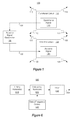
- FIG. 1 abstractly illustrates an electrical system 100 that includes a functional circuit 110 that carries one or more electrical signals 111 .
- the functional circuit 110 may be any circuit regardless of its function as all electrical circuits include one or more operational signals.
- a time-dependent current moves through an electrical conductor, the conductor emits corresponding electromagnetic radiation.
- electromagnetic interference EMI
- the functional circuit 110 emits electromagnetic interference 112 .
- the electrical system 100 also includes an antenna circuit 120 for carrying an antenna signal 121 .
- the antenna circuit 120 acts as an antenna and is present for the purpose of emitting electromagnetic radiation 122 .
- the electromagnetic radiation 122 at least partially offsets electromagnetic interference 112 emitted by an operational signal(s) 111 of the functional circuit 110 .
- the electrical system 100 also includes an antenna signal generation circuit 130 in proximity (and perhaps coupled in some embodiments) to the functional circuit 110 .
- the electrical system further is coupled to the antenna circuit 120 and generates the antenna signal 121 such that the antenna signal 121 is applied to the antenna circuit 120 as represented by arrow 132 .
- the antenna signal generation circuit 130 is coupled to the functional circuit 110 so as to access at least one of the one or more operational signals 111 of the functional circuit 110 (as represented by dashed arrow 131 ).
- square wave clock signals may often have high frequency components that emit EMI haying problematic frequency characteristics.
- the electrical system 100 may be on a single integrated circuit (e.g., on a single semiconductor die), or perhaps distributed across multiple integrated circuits (e.g., across multiple semiconductor dies) perhaps on the same circuit board or within the same packaging.
- the functional circuit 110 might be on one integrated circuit, whereas the antenna signal generation circuit 130 and antenna circuit 120 are on a separate integrated circuit, but perhaps being proximate the functional circuit 110 .
- the functional circuit 110 having the operational signal(s) 111 may be modeled as a first antenna (also referred herein as the “primary antenna”) carrying a signal having time-varying current represented herein as I 1 .
- the antenna circuit 120 having antenna signal 121 may be modeled as a second antenna (also referred to herein as the “compensating ante a”) carrying a signal having time-varying current represented herein as I 2 .
- the combination may be viewed as an antenna array in which the array has a lower radiation pattern as compared to radiation pattern of the primary antenna that models the functional circuit 110 .
- the primary antenna and the compensating antenna are modeled in the x-plane of Cartesian space, and the symbol “a” represents half the distance between the two antennas (i.e., the distance between the two antennas is 2 times “a”).
- the symbol “ ⁇ ” represents the angle between an arbitrary point “P” and the y-z plane, where “P” is assumed to be relatively far from the antennae as compared to the size of the antenna and the separate distance “2a” between the two antennas.
- the symbol “ ⁇ ” represents the angle between the point “P” and the x-y plane in the referenced Cartesian space.
- the symbol “r” represents the radial distance between the point “P” and the mid-point between the two antennas.
- the symbol “ ⁇ ” represents the characteristic impedance of the medium of the antenna.
- the symbol “k” represents the wave number of the radiation.
- the symbol “j” represents the square root of negative one, which is the imaginary constant used in complex number theory.
- the symbol “dl 1 ” represents the loop length of the primary antenna, and the symbol “dl 2 ” represents the loop length of the compensating antenna.
- the symbol “E ⁇ ” represents the electric field vector at point “P”.
- the symbol “H ⁇ ” represents the magnetic field vector at point “P”.
- I 2 the time-varying current of the compensating antenna
- I 0 the same frequency ⁇ as the primary antenna
- phase difference “ ⁇ ” as compared to the primary antenna
- ⁇ ⁇ is the complex conjugate of “E ⁇ ”.
- the electro-magnetic power of a simple two-element array can be controlled by changing: 1) ⁇ , the ratio of products of amplitude and loop length of the two signals, 2) ⁇ , the phase difference between the two signals in time-domain, and 3) 2a, the spacing between the two antenna.
- Equation 4 also permits an extension. If there is a net electro-magnetic field of a certain frequency ⁇ due to many different sources, an opposing electro-magnetic field may be created such that this net field is cancelled. Hence, even for an existing array of signals, another signal can be added and by modifying a combination of the three parameters listed above; a net zero or a reduced electromagnetic field can be produced. If the electronic system already exists, some parameters may already be fixed. For instance, as for ⁇ , the equivalent loop lengths of the functional circuit 110 and the antenna circuit 120 may be fixed but could have been taken into consideration in the design of the electrical system 100 , before the electrical system was manufactured. Also, perhaps the amplitude of the operational signals is not to be changed.
- ⁇ may be affected by changing the amplitude of the antenna signal.
- the phase of the antenna signal may be adjusted.
- 2a if the function circuit 110 and antenna circuit 110 are already fixed, 2a cannot be adjusted after manufacture of the electrical system 100 , but could be considered in the design phase of the electrical system 100 . Thus, after manufacture of the electrical system, the antenna signal may still be adjusted by changing the amplitude and phase of the antenna signal.
- FIG. 1 an example application of the principles of FIG. 1 will be described with respect to a single-ended operation signal in FIGS. 2 and 3 . Subsequent to that, an example application of the principles of FIG. 1 will be described with respect to a differential operation signal in FIGS. 4 and 5 , in both the single-ended example, and the differential example, the operational signal is used to formulate the antenna signal.
- FIGS. 6 and 7 will then be described, which describe an antenna signal generation circuit that does not use the operational signal to generate the antenna signal, but rather generates the antenna signal to offset a particular harmonic.
- FIG. 2 illustrates an example antenna signal generation circuit 200 in which the antenna generation circuit 200 uses a single-ended signal of the one or more operational signals of the functional circuit to generate the antenna signal.
- the antenna signal generation circuit 200 receives an input signal 201 .
- the input signal might be a single-ended operational signal of the functional circuit.
- the single-ended signal might be a clock signal.
- FIG. 3 illustrates signal timing diagrams for several signals involved in this example operation of the antenna signal generation circuit 200 .
- the signal 301 may be the input signal in the case of a square-wave clock signal.
- the input signal 201 is received into a delay mechanism such as an inverter/buffer that introduces a delay into the input signal 202 .
- a delay mechanism such as an inverter/buffer that introduces a delay into the input signal 202 .
- the signal 302 might represent a delayed form of the input signal 302 .
- the signal 302 is ⁇ degrees out of phase with the input signal.
- the delay control 221 provides appropriate adjustments to the phase ⁇ by signaling the inverter/buffer 211 appropriately. This phase may be adjusted at initial manufacture of the electronic system 100 and/or may be adjusted later. The phase ⁇ is thus adjusted to reduce the measured EMI of the operating circuit.
- the amplitude of the signal 302 might also be adjusted using the adjustable amplitude control 222 , which again might be performed once at fabrication, or permits one or more times thereafter to thereby reduce EMI.
- the amplitude adjustment allows for adjustment of the ⁇ factor in Equation 5.
- the antenna signal generation circuit 200 is also illustrated as being passed through a filter 212 .
- the filter 212 may be a high pass filter, a low pass filter, a bandpass filter, or the like, and is optional.
- the filter 212 acts to allow frequencies that are sensitive to EMI to be passed. By passing such frequency components into the antenna signal, the antenna signal is thereby able to counteract the EMI emitted by the operational signals 111 of the functional circuit 110 , thereby reducing EMI in the frequency components of interest.
- FIGS. 4 and 5 illustrate the application of the electrical system 100 of FIG. 1 to differential signaling.
- Many electronic systems have adopted differential signaling as signal standards.
- this array produces a much smaller electromagnetic field than that of a single signal alone.
- EMI results because of the fact that ⁇ is not exactly 180 degrees. Commonly specified as inter-pair skew, this affects the radiation at very high frequencies, where the value of ⁇ turns out to be closer to about 150 degrees.
- differential signaling may not reduce EMI and may even perhaps increase EMI.
- FIG. 4 illustrates an example antenna signal generation circuit 400 in which the antenna generation circuit 400 uses a differential signal of the one or more operational signals of the functional circuit to generate the antenna signal.
- the antenna signal generation circuit 400 for use in differential signaling is similar to the antenna signal generation circuit 200 that is used in single-ended signaling.
- the antenna signal generation circuit 400 has a common mode signal generation circuit 411 that receives a differential input signal 401 and is configured to generate a common mode signal 402 of the differential operation signal.
- FIG. 5 illustrates a signal timing diagram 500 for four signals that may be used in the antenna signal generation circuit 400 of FIG. 4 .
- Signals 511 and 512 are the two differential components of the differential input signal 401 . Note that they are not exactly 180 degrees out of phase, and thus the common mode signal 502 (which represents an example of the signal 402 of FIG. 4 ) has pulses. These pulses contribute to EMI in a differential system.
- the common mode signal 402 then acts as an input system to the inverter/buffer 412 to which appropriate delay is introduced by the adjustable delay control 421 .
- Signal 503 represents an example of the signal 403 that is output from the inverter/buffer 402 .
- Adjustable amplitude control 422 may be provided to the common mode signal generation circuit 400 of FIG. 4 . Once again, such phase and amplitude adjustments may be provided at the time of manufacture or later, and might be provided once or multiple times, and perhaps repeatedly to thereby reduce EMI emissions of the electrical system 100 .
- An optional filter 413 filters the inverted common mode signal 403 to output a filtered output signal that has frequency components that are of interested in reducing EMI.
- the output signal 404 may be the antenna signal 121 that is asserted on the antenna circuit 120 .
- a clock-generator acts as an electromagnetic transmitter.
- EMI at the clock frequency and/or one or more specific harmonics may be eliminated.
- the antenna signal can be designed to emit 532 MHz with a controllable phase. The phase can be tuned until the EMI of that harmonic is reduced to be in compliance.
- FIG. 6 illustrates an abstract block diagram of an example antenna signal generation circuit 600 .
- the antenna signal generation circuit 600 uses a timing reference 610 , rather than the operational signal(s) of the functional circuit in order to generate an offsetting electromagnetic radiation of the problematic frequency.
- the timing reference 610 may not generate the signal at the problem frequency, and so the frequency synthesis component 620 is used to generate a signal at the problematic frequency, and with the proper delay, at the direction of the delay/frequency control circuit 640 .
- the signal at the proper frequency is then subjected to filter 630 to allow the antenna signal 631 to be generated with the frequency component that is to be offset in the EMI.
- the described electrical system has a number of advances. Firstly, unlike with conventional passive filtering and spread spectrum techniques for EMI reduction, the electrical system 100 may be implemented without significantly impacting signal quality or functionality.
- the electrical system 100 may use offsetting electromagnetic radiation in combination with other EMI reduction technologies. For instance, passive filtering, spread spectrum, and shielding techniques may still be used to reduce EMI while still incorporating the principles herein.
- the principles described herein can be used to create a single antenna signal that can reduce or cancel the net of all the other signals or it can used to create an array of signals to reduce or cancel the EMI of each signal.
- the principles described herein can be used to reduce/cancel a particular frequency or a set of frequencies using a single circuit implementation.
- FIGS. 7 through 9 illustrate flowcharts of various methods for operating the electrical system 100 .
- FIG. 7 specifically illustrates a flowchart of a method 700 for operating the electrical system 100 so as to reduce EMI emissions.
- One or more of the operational signals of the functional circuit are accessed (act 701 ). This act is optional as the embodiment of FIG. 6 does not require access to an operation signal 111 of the functional circuit 110 .
- the input signal (which could be an operation signal of the functional circuit) is provided to inverter/buffer 211 .
- the differential input signal 401 is provided to the common mode generation circuit 411 .
- the antenna signal is then generated (act 702 ) using at least one operational signal of the functional circuit. For instance, in FIGS. 2 , 4 and 6 , the output signals 203 , 404 and 631 , respectively, are generated.
- the antenna signal is then applied to the antenna circuit (act 703 ).
- FIG. 8 illustrates a flowchart of a method 800 for generating the antenna signal.
- the method 800 represents an example of the act 702 of FIG. 7 .
- an input signal is optionally prepared (act 801 ) based on one or more operation signals of the functional circuit.
- the act 801 is optional in two senses.
- an operational signal is not used at all by the antenna signal generation circuit 600 .
- the single-ended signal may be used directly as an input signal without any further preparation.
- the common mode signal generation circuit 411 prepares the common mode signal.
- Delay is introduced into the signal (act 802 ) and the signal is given an appropriate amplification (act 803 ).
- this allows the antenna signal to be tailored to reduce EMI emissions under the dual antenna model.
- the adjustable delay control 221 and the adjustable amplitude control 222 are provided to the inverter/buffer 211 .
- the adjustable delay control 421 is provided to the inverter/buffer 412
- the adjustable amplitude control 422 is provided to the common mode generation circuit 411 and/or the inverter/buffer 412 .
- the delay/frequency control 640 adjusts the phase introduced by the frequency synthesis module 620 .
- the amplitude of the signal may also be adjusted by the frequency synthesis module 620 .
- the signal is then optionally filtered (act 804 ). For instance, in FIGS. 2 , 4 and 6 , this function is performed by the filters 212 , 413 and 630 , respectively.
- FIG. 9 illustrates a flowchart of a method 900 for calibrating the electrical system 100 so as to reduce electro-magnetic interference emitted by the electrical system.
- the electrical circuit is operated (act 901 ) and then calibrated while in operation (act 902 ). Specifically, one or more parameters of the antenna signal generation circuit are adjusted (act 911 ) while the effective result on EMI is measured (act 912 ). This is repeated until EMI is reduced in a desired way.
- the principles described herein permit for the effective reduction of EMI using an antenna circuit that generates opposing EMI in the problematic frequencies. This is performed without significantly affecting signal quality.
Landscapes
- Engineering & Computer Science (AREA)
- Computer Networks & Wireless Communication (AREA)
- Signal Processing (AREA)
- Near-Field Transmission Systems (AREA)
- Shielding Devices Or Components To Electric Or Magnetic Fields (AREA)
Abstract
Description
E θ =η*H Φ=(jkη/4πr)*Sin θ*e −jkr(I 1 dl 1 e jka*sin θ cos Φ +I 2 dl 2 e −jka*sin θ cos Φ) (1)
E θ=(jkη/4πr)*Sin θ*e −jkr *e −jχ/2 *I 1 dl 1*{(1+β)*cos(ka*sin θ cos Φ−χ/2)+j*(1−β)*sin(ka*sin θ cos Φ−χ/2)} (2)
E θ =E 0*{(1+β)*cos(ka*sin θ cos Φ−χ/2)+j*(1−β)*sin(ka*sin θ cos Φ−χ/2)} (3)
P=1/2η*E 0 *Ē θ, (4)
Here, “Ēθ” is the complex conjugate of “Eθ”.
P={E 0 2/2η}*{((1+β)*cos(ka*cos Φ−χ/2))2+((1−β)*sin(ka*cos Φ−χ/2))2} (5)
Claims (21)
Applications Claiming Priority (2)
| Application Number | Priority Date | Filing Date | Title |
|---|---|---|---|
| IN2551DE2010 | 2010-10-26 | ||
| IN2551/DEL/2010 | 2010-10-26 |
Publications (2)
| Publication Number | Publication Date |
|---|---|
| US20120098591A1 US20120098591A1 (en) | 2012-04-26 |
| US8643446B2 true US8643446B2 (en) | 2014-02-04 |
Family
ID=45972511
Family Applications (1)
| Application Number | Title | Priority Date | Filing Date |
|---|---|---|---|
| US13/020,443 Active 2032-04-16 US8643446B2 (en) | 2010-10-26 | 2011-02-03 | Electro-magnetic interference reduction using opposing field transmitter |
Country Status (1)
| Country | Link |
|---|---|
| US (1) | US8643446B2 (en) |
Cited By (1)
| Publication number | Priority date | Publication date | Assignee | Title |
|---|---|---|---|---|
| US20150236844A1 (en) * | 2014-02-19 | 2015-08-20 | Delta Electronics (Shanghai) Co., Ltd. | Synchronization signal transmitting device, method thereof and power electronic apparatus having the device |
Families Citing this family (2)
| Publication number | Priority date | Publication date | Assignee | Title |
|---|---|---|---|---|
| DE102017208682A1 (en) * | 2017-05-23 | 2018-11-29 | Robert Bosch Gmbh | Emission protection device and method for operating a load |
| DE102018209001A1 (en) * | 2018-06-07 | 2019-12-12 | Robert Bosch Gmbh | Control device device for a motor vehicle, motor vehicle |
Citations (4)
| Publication number | Priority date | Publication date | Assignee | Title |
|---|---|---|---|---|
| US5606734A (en) * | 1993-03-02 | 1997-02-25 | American Nucleonics Corporation | Structure generated composite reference signal for interference suppression in an adaptive loop |
| US6013957A (en) * | 1994-09-13 | 2000-01-11 | Alcatel | Arrangement for reducing the electromagnetic field created by power electronic equipment |
| US6510526B1 (en) | 1999-12-23 | 2003-01-21 | Intel Corporation | Differential clocking for digital platforms |
| US7099662B2 (en) * | 2000-11-21 | 2006-08-29 | Vega Grieshaber Kg | Transceiver unit with interference-reducing antenna |
-
2011
- 2011-02-03 US US13/020,443 patent/US8643446B2/en active Active
Patent Citations (4)
| Publication number | Priority date | Publication date | Assignee | Title |
|---|---|---|---|---|
| US5606734A (en) * | 1993-03-02 | 1997-02-25 | American Nucleonics Corporation | Structure generated composite reference signal for interference suppression in an adaptive loop |
| US6013957A (en) * | 1994-09-13 | 2000-01-11 | Alcatel | Arrangement for reducing the electromagnetic field created by power electronic equipment |
| US6510526B1 (en) | 1999-12-23 | 2003-01-21 | Intel Corporation | Differential clocking for digital platforms |
| US7099662B2 (en) * | 2000-11-21 | 2006-08-29 | Vega Grieshaber Kg | Transceiver unit with interference-reducing antenna |
Non-Patent Citations (2)
| Title |
|---|
| Kyle Swartz, et al., "High Frequency PCB Layout", Bosch, Invented for Life, Mar. 24, 2008, http://www.egr.msu.edu/classes/ece480/goodman/spring08/group05/docs/High-Freq-PCBlayout.pdf (17 pages). |
| Kyle Swartz, et al., "High Frequency PCB Layout", Bosch, Invented for Life, Mar. 24, 2008, http://www.egr.msu.edu/classes/ece480/goodman/spring08/group05/docs/High—Freq—PCBlayout.pdf (17 pages). |
Cited By (2)
| Publication number | Priority date | Publication date | Assignee | Title |
|---|---|---|---|---|
| US20150236844A1 (en) * | 2014-02-19 | 2015-08-20 | Delta Electronics (Shanghai) Co., Ltd. | Synchronization signal transmitting device, method thereof and power electronic apparatus having the device |
| US10547437B2 (en) * | 2014-02-19 | 2020-01-28 | Delta Electronics (Shanghai) Co., Ltd. | Synchronization signal transmitting device, method thereof and power electronic apparatus having the device |
Also Published As
| Publication number | Publication date |
|---|---|
| US20120098591A1 (en) | 2012-04-26 |
Similar Documents
| Publication | Publication Date | Title |
|---|---|---|
| Mardiguian et al. | Controlling radiated emissions by design | |
| US8004330B1 (en) | Reduction of electromagnetic interference for differential signals | |
| US7956704B1 (en) | Loaded parallel stub common mode filter for differential lines carrying high rate digital signals | |
| US5909472A (en) | Digital circuit clocking using a dual side band suppressed carrier clock modulated signal | |
| US10644670B2 (en) | Radiofrequency filter with improved attenuation of common mode signals | |
| US8643446B2 (en) | Electro-magnetic interference reduction using opposing field transmitter | |
| Barbuto et al. | Waveguide components and aperture antennas with frequency-and time-domain selectivity properties | |
| US20130027255A1 (en) | Radio apparatus | |
| US9130650B1 (en) | Transformer based circuit for reducing EMI radiation in high speed CMOS SERDES transmitters | |
| US9369114B2 (en) | EMI control method and apparatus, and electronic device | |
| Kwon et al. | Partial EBG structure with decap for ultra‐wideband suppression of simultaneous switching noise in a high‐speed system | |
| Xiao et al. | Simulation analysis of electromagnetic shielding of electronic device chassis | |
| Abubakar et al. | Interference and electromagnetic compatibility challenges in 5G wireless network deployments | |
| Zhechev | Experimental study of the buried vias effect on reflection symmetric modal filter performance | |
| Rohde et al. | Electromagnetic interference and start-up dynamics in high frequency crystal oscillator circuits | |
| CN106656115B (en) | Long-distance clock signal EMI suppression circuit | |
| Maqbool et al. | EMI-related common-mode (CM) noise analysis and prediction of high-speed source-series terminated (SST) I/O driver in system-on-package (SOP) | |
| Chen et al. | Improving the electromagnetic compatibility of electronic products by using response surface methodology and artificial neural network | |
| Maheswari et al. | Simulation and Measurement of Conducted Emission in DC-DC convertor | |
| Kostka et al. | Modeling of RF desense for mobile electronics | |
| Arihilam | Measurement of Electromagnetic Noise Coupling and Signal Mode Conversion in Data Cabling | |
| Abdullah et al. | Performance study of egg tray microwave absorber | |
| Keller | Noise Coupling | |
| Yi et al. | Exploring the Effectiveness of Thin Microwave Absorber Applied in Parallel-Plate Waveguide | |
| JP6573326B2 (en) | Wireless communication apparatus and noise suppression method |
Legal Events
| Date | Code | Title | Description |
|---|---|---|---|
| AS | Assignment |
Owner name: SEMICONDUCTOR COMPONENTS INDUSTRIES, LLC, ARIZONA Free format text: ASSIGNMENT OF ASSIGNORS INTEREST;ASSIGNORS:SUBRAMANIAN, HARIHARA;SINGH, GAUTAM K.;REEL/FRAME:025959/0768 Effective date: 20110315 |
|
| STCF | Information on status: patent grant |
Free format text: PATENTED CASE |
|
| AS | Assignment |
Owner name: DEUTSCHE BANK AG NEW YORK BRANCH, NEW YORK Free format text: SECURITY INTEREST;ASSIGNOR:SEMICONDUCTOR COMPONENTS INDUSTRIES, LLC;REEL/FRAME:038620/0087 Effective date: 20160415 |
|
| AS | Assignment |
Owner name: DEUTSCHE BANK AG NEW YORK BRANCH, AS COLLATERAL AGENT, NEW YORK Free format text: CORRECTIVE ASSIGNMENT TO CORRECT THE INCORRECT PATENT NUMBER 5859768 AND TO RECITE COLLATERAL AGENT ROLE OF RECEIVING PARTY IN THE SECURITY INTEREST PREVIOUSLY RECORDED ON REEL 038620 FRAME 0087. ASSIGNOR(S) HEREBY CONFIRMS THE SECURITY INTEREST;ASSIGNOR:SEMICONDUCTOR COMPONENTS INDUSTRIES, LLC;REEL/FRAME:039853/0001 Effective date: 20160415 Owner name: DEUTSCHE BANK AG NEW YORK BRANCH, AS COLLATERAL AG Free format text: CORRECTIVE ASSIGNMENT TO CORRECT THE INCORRECT PATENT NUMBER 5859768 AND TO RECITE COLLATERAL AGENT ROLE OF RECEIVING PARTY IN THE SECURITY INTEREST PREVIOUSLY RECORDED ON REEL 038620 FRAME 0087. ASSIGNOR(S) HEREBY CONFIRMS THE SECURITY INTEREST;ASSIGNOR:SEMICONDUCTOR COMPONENTS INDUSTRIES, LLC;REEL/FRAME:039853/0001 Effective date: 20160415 |
|
| FPAY | Fee payment |
Year of fee payment: 4 |
|
| MAFP | Maintenance fee payment |
Free format text: PAYMENT OF MAINTENANCE FEE, 8TH YEAR, LARGE ENTITY (ORIGINAL EVENT CODE: M1552); ENTITY STATUS OF PATENT OWNER: LARGE ENTITY Year of fee payment: 8 |
|
| AS | Assignment |
Owner name: FAIRCHILD SEMICONDUCTOR CORPORATION, ARIZONA Free format text: RELEASE OF SECURITY INTEREST IN PATENTS RECORDED AT REEL 038620, FRAME 0087;ASSIGNOR:DEUTSCHE BANK AG NEW YORK BRANCH, AS COLLATERAL AGENT;REEL/FRAME:064070/0001 Effective date: 20230622 Owner name: SEMICONDUCTOR COMPONENTS INDUSTRIES, LLC, ARIZONA Free format text: RELEASE OF SECURITY INTEREST IN PATENTS RECORDED AT REEL 038620, FRAME 0087;ASSIGNOR:DEUTSCHE BANK AG NEW YORK BRANCH, AS COLLATERAL AGENT;REEL/FRAME:064070/0001 Effective date: 20230622 |