US8638043B2 - Two-terminal current controller and related LED lighting device - Google Patents

Two-terminal current controller and related LED lighting device Download PDF

Info

Publication number
US8638043B2
US8638043B2 US13/052,132 US201113052132A US8638043B2 US 8638043 B2 US8638043 B2 US 8638043B2 US 201113052132 A US201113052132 A US 201113052132A US 8638043 B2 US8638043 B2 US 8638043B2
Authority
US
United States
Prior art keywords
voltage
current
reference voltage
current controller
terminal current
Prior art date
Legal status (The legal status is an assumption and is not a legal conclusion. Google has not performed a legal analysis and makes no representation as to the accuracy of the status listed.)
Active, expires
Application number
US13/052,132
Other versions
US20120139448A1 (en
Inventor
Yung-Hsin Chiang
Yi-Mei Li
Current Assignee (The listed assignees may be inaccurate. Google has not performed a legal analysis and makes no representation or warranty as to the accuracy of the list.)
Iml Hong Kong Ltd
Original Assignee
IML International
Priority date (The priority date is an assumption and is not a legal conclusion. Google has not performed a legal analysis and makes no representation as to the accuracy of the date listed.)
Filing date
Publication date
Application filed by IML International filed Critical IML International
Assigned to ADDTEK CORP. reassignment ADDTEK CORP. ASSIGNMENT OF ASSIGNORS INTEREST (SEE DOCUMENT FOR DETAILS). Assignors: CHIANG, YUNG-HSIN, LI, YI-MEI
Assigned to IML INTERNATIONAL reassignment IML INTERNATIONAL ASSIGNMENT OF ASSIGNORS INTEREST (SEE DOCUMENT FOR DETAILS). Assignors: ADDTEK CORP
Publication of US20120139448A1 publication Critical patent/US20120139448A1/en
Priority to US13/743,345 priority Critical patent/US8638047B2/en
Application granted granted Critical
Publication of US8638043B2 publication Critical patent/US8638043B2/en
Assigned to IML HONG KONG LIMITED reassignment IML HONG KONG LIMITED ASSIGNMENT OF ASSIGNORS INTEREST (SEE DOCUMENT FOR DETAILS). Assignors: IML INTERNATIONAL
Active legal-status Critical Current
Adjusted expiration legal-status Critical

Links

Images

Classifications

    • HELECTRICITY
    • H05ELECTRIC TECHNIQUES NOT OTHERWISE PROVIDED FOR
    • H05BELECTRIC HEATING; ELECTRIC LIGHT SOURCES NOT OTHERWISE PROVIDED FOR; CIRCUIT ARRANGEMENTS FOR ELECTRIC LIGHT SOURCES, IN GENERAL
    • H05B45/00Circuit arrangements for operating light-emitting diodes [LED]
    • H05B45/40Details of LED load circuits
    • H05B45/44Details of LED load circuits with an active control inside an LED matrix
    • H05B45/48Details of LED load circuits with an active control inside an LED matrix having LEDs organised in strings and incorporating parallel shunting devices
    • HELECTRICITY
    • H02GENERATION; CONVERSION OR DISTRIBUTION OF ELECTRIC POWER
    • H02MAPPARATUS FOR CONVERSION BETWEEN AC AND AC, BETWEEN AC AND DC, OR BETWEEN DC AND DC, AND FOR USE WITH MAINS OR SIMILAR POWER SUPPLY SYSTEMS; CONVERSION OF DC OR AC INPUT POWER INTO SURGE OUTPUT POWER; CONTROL OR REGULATION THEREOF
    • H02M7/00Conversion of ac power input into dc power output; Conversion of dc power input into ac power output
    • H02M7/02Conversion of ac power input into dc power output without possibility of reversal
    • H02M7/04Conversion of ac power input into dc power output without possibility of reversal by static converters
    • H02M7/06Conversion of ac power input into dc power output without possibility of reversal by static converters using discharge tubes without control electrode or semiconductor devices without control electrode

Definitions

  • the present invention is related to a two-terminal current controller and related LED lighting device, and more particularly, to a two-terminal current controller and related LED lighting device with high power factor.
  • LEDs light-emitting diodes
  • LEDs are advantageous in low power consumption, long lifetime, small size, no warm-up time, fast reaction speed, and the ability to be manufactured as small or array devices.
  • LEDs are also widely used as indoor/outdoor lighting devices in place of fluorescent or incandescent lamps.
  • FIG. 1 is a diagram illustrating the voltage-current chart of a light-emitting diode.
  • the forward-bias voltage of the light-emitting diode When the forward-bias voltage of the light-emitting diode is smaller than its barrier voltage Vb, the light-emitting diode functions as an open-circuited device since it only conducts a negligible amount of current.
  • the forward-bias voltage of the light-emitting diode exceeds its barrier voltage Vb, the light-emitting diode functions as a short-circuited device since its current increases exponentially with the forward-bias voltage.
  • the barrier voltage Vb whose value is related to the material and doping type of the light-emitting diode, is typically between 1.5 and 3.5 volts. For most current values, the luminescence of the light-emitting diode is proportional to the current. Therefore, a current source is generally used for driving light-emitting diodes in order to provide uniform lumin
  • FIG. 2 is a diagram of a prior art LED lighting device 600 .
  • the LED lighting device 600 includes a power supply circuit 110 , a resistor R and a luminescent device 10 .
  • the power supply circuit 110 is configured to receive an alternative-current (AC) voltage VS having positive and negative periods and convert the output of the AC voltage VS in the negative period using a bridge rectifier 112 , thereby providing a rectified AC voltage V AC for driving the luminescent device 10 .
  • the resistor R is coupled in series with the luminescent device 10 for regulating its current I LED . In many applications, multiple light-emitting diodes are required in order to provide sufficient brightness.
  • the luminescent device 10 Since a light-emitting diode is a current-driven device whose luminescence is proportional to its driving current, the luminescent device 10 normally adopts a plurality of light-emitting diodes D 1 -D n coupled in series. Assuming that the barrier voltage of all the light-emitting diodes D 1 -D n is equal to the ideal value Vb and the rectified AC voltage V AC periodically varies between 0 and V MAX , a forward-bias voltage larger than n*Vb is required for turning on the luminescent device 10 . Therefore, the energy between 0 and n*Vb can not be used.
  • the prior art LED lighting device 600 needs to make compromise between the effective operational voltage range and the reliability. Meanwhile, the current-limiting resistor R also consumes extra power and may thus lower system efficiency.
  • FIG. 3 is a diagram of another prior art LED lighting device 700 .
  • the LED lighting device 700 includes a power supply circuit 110 , an inductor L, a capacitor C, a switch SW, and a luminescent device 10 .
  • the power supply circuit 110 is configured to receive an AC voltage VS having positive and negative periods and convert the output of the AC voltage VS in the negative period using a bridge rectifier 112 , thereby providing a rectified AC voltage V AC for driving the luminescent device 10 .
  • the inductor L and the switch SW are coupled in series with the luminescent device 10 for limiting its current I LED .
  • the capacitor C is coupled in parallel with the luminescent device 10 for absorbing voltage ripples of the power supply circuit 110 .
  • the inductor L consumes less energy than the resistor R of the LED lighting device 600 .
  • the inductor L for regulating current and the capacitor for stabilizing voltage largely reduce the power factor of the LED lighting device 700 and the energy utilization ratio. Therefore, the prior art LED lighting device 700 needs to make compromise between the effective operational voltage range and the brightness.
  • the present invention provides an LED lighting device comprising a luminescent device configured to provide light according to a first current and a two-terminal current controller coupled in parallel with the luminescent device and configured to regulate the first current according to a voltage established across the luminescent device.
  • the two-terminal current controller operates in a first mode.
  • the two-terminal current controller operates in a second mode.
  • the two-terminal current controller operates in a third mode.
  • the two-terminal current controller includes a current limiting unit and an adjusting unit.
  • the current limiting unit is configured to conduct a second current associated with the rectified AC voltage, regulate the second current according to the voltage established across the luminescent device and maintain the first current at zero when the two-terminal current controller operates in the first mode; conduct the second current, maintain the second current at a first predetermined value larger than zero and maintain the first current at zero when the two-terminal current controller operates in the second mode; and switch off when the two-terminal current controller operates in the third mode.
  • the adjusting unit is configured to adjust the first predetermined value and the second voltage.
  • the present invention also provides two-terminal current controller for controlling a first current passing through a load.
  • the two-terminal current controller operates in a first mode.
  • the two-terminal current controller operates in a second mode.
  • the two-terminal current controller operates in a third mode.
  • the two-terminal current controller includes a current limiting unit and an adjusting unit.
  • the current limiting unit is configured to conduct a second current associated with the rectified AC voltage, regulate the second current according to the voltage established across the load and maintain the first current at zero when the two-terminal current controller operates in the first mode; conduct the second current, maintain the second current at a predetermined value larger than zero and maintain the first current at zero when the two-terminal current controller operates in the second mode; and switch off when the two-terminal current controller operates in the third mode.
  • the adjusting unit is configured to adjust the predetermined value and the second voltage.
  • FIG. 1 is a diagram illustrating the voltage-current chart of a light-emitting diode.
  • FIGS. 2 and 3 are diagrams of prior art LED lighting devices.
  • FIGS. 4 , 7 , 10 , 13 and 15 are diagrams of LED lighting devices according to embodiments of the present invention.
  • FIGS. 5 , 8 and 11 A- 11 D are diagrams illustrating the current-voltage chart of a two-terminal current controller according to the present invention.
  • FIGS. 6 , 9 , 12 and 14 are diagrams illustrating the variations in the related current and voltage when operating the LED lighting device of the present invention.
  • FIGS. 16 and 17 are diagrams of illustrated embodiments of the two-terminal current controller.
  • FIG. 4 is a diagram of an LED lighting device 100 according to a first embodiment of the present invention.
  • the LED lighting device 100 includes a power supply circuit 110 , a two-terminal current controller 120 , and a luminescent device 10 .
  • the power supply circuit 110 is configured to receive an AC voltage VS having positive and negative periods and convert the output of the AC voltage VS in the negative period using a bridge rectifier 112 , thereby providing a rectified AC voltage V AC , whose value varies periodically with time, for driving the luminescent device 10 .
  • the luminescent device 10 may adopt n light-emitting units D 1 -D n coupled in series, each of which may include a single light-emitting diode or multiple light-emitting diodes.
  • FIG. 1 light-emitting units
  • the two-terminal current controller 120 coupled in parallel with the luminescent device 10 and the power supply circuit 110 , includes a current limiting unit 120 A and an adjusting unit 120 B.
  • the two-terminal current controller 120 is configured to control the current I LED passing through the luminescent device 10 according to the rectified AC voltage V AC , wherein I AK represents the current passing through the current limiting unit 120 A and V AK represents the voltage established across the current limiting unit 120 A.
  • the barrier voltage Vb′ of the two-terminal current controller 120 is smaller than the overall barrier voltage n*Vb of the luminescent device 10 (assuming the barrier voltage of each light-emitting unit is equal to Vb).
  • FIGS. 5 and 6 illustrate the operation of the LED lighting device 100 , wherein FIG. 5 is a diagram illustrating the current-voltage chart of the two-terminal current controller 120 , and FIG. 6 is a diagram illustrating the variations in the related current and voltage when operating the LED lighting device 100 .
  • the vertical axis represents the current I AK passing through the current limiting unit 120 A
  • the horizontal axis represents the voltage V AK established across the current limiting unit 120 A.
  • the two-terminal current controller 120 operates in a first mode in which the current limiting unit 120 A functions as a voltage-controlled device when 0 ⁇ V AK ⁇ V DROP .
  • the current I AK changes with the voltage V AK in a specific manner.
  • the two-terminal current controller 120 operates in a second mode in which the current limiting unit 120 A functions as a constant current source when V DROP ⁇ V AK ⁇ V OFF — TH ′.
  • the current I AK is maintained at an adjustable specific current I MAX ′ instead of changing with the voltage V AK .
  • the two-terminal current controller 120 functions in a third mode in which the current limiting unit 120 A is turned off when V AK >V OFF — TH ′.
  • the two-terminal current controller 120 functions as an open-circuited device since the current I AK is suddenly reduced to zero.
  • the adjusting unit 120 B may provide flexible designs with various characteristics by adjusting the value of I MAX ′ when the two-terminal current controller 120 operates in the second mode and the value of V OFF — TH ′ for switching between the second mode and the third mode.
  • FIG. 6 illustrates the waveforms of the voltage V AK , the current I AK and the current I LED . Since the voltage V AK is associated with the rectified AC voltage V AC whose value varies periodically with time, a cycle between t 0 -t 6 is used for illustration, wherein the period between t 0 -t 3 is the rising period of the rectified AC voltage V AC and the period between t 4 -t 6 is the falling period of the rectified AC voltage V AC . Between t 0 -t 1 when the voltage V AK gradually increases, the current limiting unit 120 A of the two-terminal current controller 120 is first turned on, after which the current I AK increases with the voltage V AK in a specific manner and the current I LED is maintained at zero.
  • the current limiting unit 120 A of the two-terminal current controller 120 is configured to limit the current I AK to a specific current I MAX ′, and the current I LED remains zero since the luminescent device 10 is still turned off.
  • the current limiting unit 120 A of the two-terminal current controller 120 is turned off and the current associated with the rectified AC voltage V AC thus flows through the luminescent device 10 . Therefore, the current I AK is reduced to zero, and the current I LED changes with the voltage V AK .
  • the current limiting unit 120 A of the two-terminal current controller 120 is turned on, thereby limiting the current I AK to the specific current I MAX ′ and maintaining the current I LED at zero again.
  • the current I AK decreases with the voltage V AK in a specific manner.
  • the two-terminal current controller 120 operates in the first mode during t 0 -t 1 and t 5 -t 6 when 0 ⁇ V AK ⁇ V DROP ; the two-terminal current controller 120 operates in the second mode during t 1 -t 2 and t 4 -t 5 when V DROP ⁇ V AK ⁇ V OFF — TH ′; the two-terminal current controller 120 operates in the third mode during t 2 -t 4 when V AK >V OFF — TH ′.
  • FIG. 7 is a diagram of an LED lighting device 200 according to a second embodiment of the present invention.
  • the LED lighting device 200 includes a power supply circuit 110 , a two-terminal current controller 120 , and a luminescent device 20 . Having similar structures, the first and second embodiments of the present invention differ in the luminescent device 20 and how it is connected to the two-terminal current controller 120 .
  • the luminescent device 20 includes two luminescent elements 21 and 25 : the luminescent element 21 is coupled in parallel to the two-terminal current controller 120 and includes m light-emitting units D 1 -D m coupled in series, wherein I LED — AK represents the current flowing through the luminescent element 21 and V AK represents the voltage established across the luminescent element 21 ; the luminescent element 25 is coupled in series to the two-terminal current controller 120 and includes n light-emitting units D 1 -D n coupled in series, wherein I LED represents the current flowing through the luminescent element 25 and V LED represents the voltage established across the luminescent element 25 .
  • Each light-emitting unit may include a single light-emitting diode or multiple light-emitting diodes.
  • FIG. 7 depicts the embodiment using a single light-emitting diode.
  • the two-terminal current controller 120 is configured to regulate the current flowing through the luminescent device 20 according to the rectified AC voltage V AC , wherein I AK represents the current flowing through the current limiting unit 120 A and V AK represents the voltage established across the current limiting unit 120 A.
  • the barrier voltage Vb′ of the current limiting unit 120 A is smaller than the overall barrier voltage m*Vb of the luminescent element 21 (assuming the barrier voltage of each luminescent element is equal to Vb).
  • FIGS. 8 and 9 illustrate the operation of the LED lighting device 200 according to the second embodiment of the present invention, wherein FIG. 8 is a diagram illustrating the current-voltage chart of the two-terminal current controller 120 , and FIG. 9 is a diagram illustrating the variations in the related current and voltage when operating the LED lighting device 200 .
  • the vertical axis represents the current I AK passing through the current limiting unit 120 A, and the horizontal axis represents the voltage V AK established across the two-terminal current controller 120 .
  • the two-terminal current controller 120 operates in the first mode in which the current limiting unit 120 A functions as a voltage-controlled device when 0 ⁇ V AK ⁇ V DROP .
  • the current I AK changes with the voltage V AK in a specific manner.
  • the two-terminal current controller 120 operates in the second mode in which the current limiting unit 120 A functions as a constant current source when V DROP ⁇ V AK ⁇ V OFF — TH ′.
  • the current I AK is maintained at an adjustable specific current I MAX ′ instead of changing with the voltage V AK .
  • the two-terminal current controller 120 operates in the third mode in which the current limiting unit 120 A is turned off when V AK >V OFF — TH ′. In other words, the two-terminal current controller 120 functions as an open-circuited device since the current I AK is suddenly reduced to zero.
  • the two-terminal current controller 120 operates in the second mode in which the current limiting unit 120 A is turned on for limiting the current I AK to the specific current I MAX ′ when V AK ⁇ V ON — TH ′.
  • the two-terminal current controller 120 operates in the first mode in which the current limiting unit 120 A functions as a voltage-controlled device when 0 ⁇ V AK ⁇ V DROP .
  • the current I AK changes with the voltage V AK in a specific manner.
  • the adjusting unit 120 B may provide flexible designs with various characteristics by adjusting the value of I MAX ′ when the two-terminal current controller 120 operates in the second mode and the value of V OFF — TH ′ for switching between the second mode and the third mode.
  • FIG. 9 illustrates the waveforms of the voltage V AC , V AK , V LED and the current I AK , I LED — AK and I LED .
  • V AC the rectified AC voltage
  • V AK the voltage V AK established across the two-terminal current controller 120
  • V LED the voltage V LED established across the n serially-coupled light-emitting units D 1 -D n increase with the rectified AC voltage V AC .
  • the current limiting unit 120 A of the two-terminal current controller 120 is first turned on, after which the current I AK and the current I LED increase with the voltage V AK in a specific manner and the current I LED — AK is maintained at zero.
  • the two-terminal current controller 120 is configured to limit the current I AK to the specific current I MAX ′, and the current I LED remains zero since the luminescent element 21 is still turned off.
  • V F representing the forward-bias voltage of each light-emitting unit in the luminescent element 25
  • the value of the voltage V LED may be represented by m*V F . Therefore, the luminescent element 21 is not conducting between t 0 -t 2 , and the rectified AC voltage V AC provided by the power supply circuit 110 is applied to the two-terminal current controller 120 and the n light-emitting units in the luminescent element 25 .
  • the two-terminal current controller 120 is turned off and the current associated with the rectified AC voltage V AC thus passes through the luminescent elements 21 and 25 .
  • the current I AK is reduced to zero, and the current I LED — AK changes with the voltage V AK . Therefore, when the luminescent element 21 is conducting between t 2 and t 4 , the voltage V AK established across the two-terminal current controller 120 is supplied as the luminescent device 20 performs voltage dividing on the rectified AC voltage V AC .
  • the two-terminal current controller 120 is turned on, thereby limiting the current I AK to the specific current I MAX ′ and maintaining the current I LED — AK at zero again.
  • the current I AK decreases with the voltage V AK in a specific manner. As depicted in FIGS. 7 and 9 , the value of the current I LED is the sum of the current I LED — AK and the current I AK .
  • the two-terminal current controller 120 may increase the effective operational voltage range (such as the output of the rectified AC voltage V AC during t 0 -t 2 and t 4 -t 6 ), thereby increasing the power factor of the LED luminescence device 200 .
  • FIG. 10 is a diagram of an LED lighting device 300 according to a third embodiment of the present invention.
  • the LED lighting device 300 includes a power supply circuit 110 , a plurality of two-terminal current controllers, and a luminescent device 30 .
  • the second and the third embodiments of the present invention differ in that the LED lighting device 300 includes a plurality of two-terminal current controllers (4 two-terminal current controllers 121 - 124 are depicted in FIG. 10 for illustration) and the luminescent device 30 includes a plurality of luminescent elements (5 luminescent elements 21 - 24 are depicted in FIG. 10 for illustration).
  • the luminescent elements 21 - 24 are each coupled in parallel to the corresponding two-terminal current controllers 121 - 124 and each include a plurality of light-emitting units coupled in series, wherein I LED — AK1 -I LED — AK4 respectively represent the currents flowing through the luminescent elements 21 - 24 and V AK1 -V AK4 respectively represent the voltages established across the luminescent elements 21 - 24 .
  • the luminescent element 25 is coupled in series to the two-terminal current controllers 121 - 124 and includes a plurality of light-emitting units coupled in series, wherein I LED represents the current flowing through the luminescent element 25 and V LED represents the voltage established across the luminescent element 25 .
  • Each light-emitting unit may include a single light-emitting diode or multiple light-emitting diodes.
  • FIG. 10 depicts the embodiment using a single light-emitting diode.
  • the two-terminal current controllers 121 - 124 each including corresponding current limiting units 121 A- 124 A and corresponding adjusting units 121 B- 124 B, are configured to regulate the currents flowing through the corresponding luminescent devices 21 - 24 according to the voltages V AK1 -V AK4 , respectively, wherein I AK1 -I AK4 respectively represent the currents flowing through the current limiting units 121 A- 124 A and V AK1 -V AK4 respectively represent the voltages established across the current limiting units 121 A- 124 A.
  • the barrier voltages of the current limiting units 121 A- 124 A are smaller than the overall barrier voltages of the corresponding luminescent elements 21 - 24 .
  • FIGS. 11A-11D and 12 illustrate the operation of the LED lighting device 300 , wherein FIG. 11A-11D are diagrams illustrating the current-voltage charts of the current limiting units 121 A- 124 A, and FIG. 12 is a diagram illustrating the variations in the related current and voltage when operating the LED lighting device 300 .
  • the adjusting units 121 B- 124 B may provide flexible designs with various characteristics by adjusting the value of I MAX ′ when the two-terminal current controllers 121 - 124 operate in the second mode and the values of V ON — TH ′ and V OFF — TH ′ for switching between the second mode and the third mode. In the embodiment illustrated in FIGS.
  • I MAX1 ⁇ I MAX2 ⁇ I MAX3 ⁇ I MAX4 V ON — TH1 ⁇ V ON — TH2 ⁇ V ON — TH3 ⁇ V ON — TH4 , and V OFF — TH1 ⁇ V OFF — TH2 ⁇ V OFF — TH3 ⁇ V OFF — TH4 .
  • FIG. 12 illustrates the waveforms of the voltage V AC and the current I LED when operating the LED lighting device 300 . Since the value of the rectified AC voltage V AC varies periodically with time, a cycle between t 0 -t 10 is used for illustration, wherein the period between t 0 -t 5 is the rising period of the rectified AC voltage V AC and the period between t 5 -t 10 is the falling period of the rectified AC voltage V AC .
  • the operation of the LED lighting device 300 during the rising period t 0 -t 5 is hereby explained.
  • the current limiting units 124 A- 121 A are sequentially turned on at t 6 -t 9 , respectively.
  • the operation of the LED lighting device 300 during the falling period t 5 -t 10 is similar to that during the corresponding rising period t 0 -t 5 as previously illustrated.
  • the luminescent element 25 has the longest conducting time
  • the luminescent element 21 has the second longest conducting time
  • the luminescent element 24 has the shortest conducting time.
  • the luminescent elements 21 - 24 may be required to provide different luminescence or become luminescent at different time.
  • the present invention may thus provide flexible designs using the adjusting units 121 B- 124 B.
  • FIG. 13 is a diagram of an LED lighting device 400 according to a fourth embodiment of the present invention.
  • the LED lighting device 400 includes a power supply circuit 110 , a plurality of two-terminal current controllers, and a luminescent device 40 . Having similar structure as the third embodiment, the LED lighting device 400 also include a plurality of two-terminal current controllers (5 two-terminal current controllers 121 - 125 are depicted in FIG. 13 for illustration) and a plurality of luminescent elements (4 luminescent elements 21 - 24 are depicted in FIG.
  • the two-terminal current controllers 121 - 124 are each coupled in parallel to the corresponding luminescent elements 21 - 24 and the two-terminal current controller 125 is coupled in series to the luminescent elements 21 - 24 .
  • FIG. 14 shows the waveforms of the voltage and the current for illustrating the operation of the LED lighting device 400 according to the fourth embodiment of the present invention.
  • the two-terminal current controllers 121 - 124 are turned off during t 4 -t 5 , and the current I LED passing through the luminescent elements 21 - 24 is determined by the rectified AC voltage V AC provided by the power supply circuit 110 .
  • the current I LED may exceed the maximum operational current of the luminescent elements 21 - 25 and thus cause permanent damages to the devices.
  • the two-terminal current controller 125 is configured to maintain the current I LED to a specific value I MAX5 which may be adjusted in various applications.
  • I MAX1 -I MAX5 depicted in FIG. 14 is only for illustrative purpose.
  • FIG. 15 is a diagram of an LED lighting device 500 according to a fifth embodiment of the present invention.
  • the LED lighting device 500 includes a power supply circuit 410 , a two-terminal current controller 120 , and a luminescent device 10 . Having similar structures, the first and fifth embodiments of the present invention differ in the power supply circuits.
  • the power supply circuit 110 is configured to rectify the AC voltage VS (such as 110-220V main) using the bridge rectifier 112 , thereby providing the rectified AC voltage V AC whose value varies periodically with time.
  • the power supply circuit 410 is configured to receive any AC voltage VS, perform voltage conversion using an AC-AC converter 412 , and rectify the converted AC voltage VS using the bridge rectifier 112 , thereby providing the rectified AC voltage V AC whose value varies periodically with time. References may be also be made to FIGS. 5 and 6 for illustrating the operation of the LED lighting device 500 . Similarly, the second to fourth embodiments of the present invention may also use the power supply circuit 410 for providing the rectified AC voltage V AC .
  • FIGS. 16 and 17 are diagrams of illustrated embodiments of the two-terminal current controller 120 .
  • the current limiting unit 120 A of the two-terminal current controller 120 includes resistors R 1 -R 7 , a switch QN, a comparator CP 1 , a band-gap reference voltage generator 50 , and a voltage-detecting circuit 70 .
  • the band-gap reference voltage generator 50 generally adopts devices having positive and negative temperature coefficients in order to achieve temperature-independent output characteristic, thereby providing a stable reference voltage V REF .
  • the resistor R 1 is used for detecting the current flowing through the switch QN, thereby providing a corresponding feedback voltage V FB .
  • the resistors R 2 -R 4 forms a voltage-dividing circuit which provides a reference voltage V REF1 and a reference voltage V REF2 according to the reference voltage V REF .
  • the comparator CP 1 having a positive input end for receiving the reference voltage V REF1 and a negative input end for receiving the feedback voltage V FB , is configured to output a control signal V g to the switch QN according to the relationship between the reference voltage V REF1 and the feedback voltage V FB .
  • the switch QN may include a field effect transistor (FET), a bipolar junction transistor (BJT) or other devices having similar function.
  • FET field effect transistor
  • BJT bipolar junction transistor
  • NMOS N-type metal-oxide-semiconductor
  • the drain-to-source voltage V DS of the switch QN increases with the voltage V AK .
  • the voltage V AK does not exceed V DROP
  • the drain-to-source voltage V DS is smaller than the difference between the gate-to-source voltage V GS and the threshold voltage V TH (V DS ⁇ V GS ⁇ V TH ).
  • the comparator CP 1 provides the control signal V g which allows the switch QN to operate in the linear region where the drain current is mainly determined by the drain-to-source voltage V DS .
  • the two-terminal current controller 120 is configured to provide the current I AK and voltage V AK whose relationship corresponds to the I-V characteristic of the switch QN when operating in the linear region.
  • the drain-to-source voltage V DS is larger than the difference between the gate-to-source voltage V GS and the threshold voltage V TH (V DS >V GS ⁇ V TH ).
  • the comparator CP 1 provides the control signal V g which results in V GS >V TH , thereby allowing the switch QN to operate in the saturation region.
  • the drain current of the comparator CP 1 is only related to the gate-to-source voltage V GS . In other words, the current I AK does not change with the voltage V AK .
  • the voltage-detecting circuit 70 includes a logic circuit 72 , a voltage edge-detecting circuit 74 , and two comparators CP 2 and CP 3 .
  • the comparator CP 2 having a positive input end for receiving the reference voltage V REF2 and a negative input end for receiving a voltage V ON , is configured to output a control signal V ON — TH ′ according to the relationship between the voltage V ON and the reference voltage V REF2 .
  • the comparator CP 3 having a positive input end for receiving a voltage V OFF and a negative input end for receiving the reference voltage V REF2 , is configured to output a control signal V OFF — TH ′ according to the relationship between the voltage V OFF and the reference voltage V REF2 .
  • the comparator CP 2 may determine the relationship between the voltages V AK and V ON — TH ′, while the comparator CP 3 may determine the relationship between the voltages V AK and V OFF — TH ′. Meanwhile, when the voltages V AK is between V OFF — TH ′ and V ON — TH ′, the voltage edge-detecting circuit 74 is configured to determine whether the rectified AC voltage V AC is during the rising period or during the falling period. Based on the results of the voltage edge-detecting circuit 74 and the comparators CP 2 and CP 3 , the logic circuit 72 outputs a corresponding control signal to the comparator CP 1 .
  • the comparator CP 1 During the rising period of the rectified AC voltage V AC when the voltage V AK is between V OFF — TH ′ and V ON — TH ′, the comparator CP 1 provides the control signal V g smaller than the threshold voltage V TH , thereby turning off the switch QN and maintaining the current I AK at zero. During the falling period of the rectified AC voltage V AC when the voltage V AK is between V ON — TH ′ and V OFF — TH ′, the comparator CP 1 provides the control signal V g larger than the threshold voltage V TH ′, thereby operating the switch QN in the saturation region and maintaining the current I AK at I MAX ′.
  • the adjusting unit 120 B includes a resistor R 8 whose value may be varied for adjusting how the reference voltage V REF is provided to the comparators CP 1 -CP 3 by voltage division.
  • the values of the reference voltages V REF1 and V REF2 may be adjusted flexibly.
  • the comparator CP 1 is configured to output the control signal V g to the switch QN according to the relationship between the reference voltage V REF1 and the feedback voltage V FB
  • the comparator CP 2 is configured to output the control signal V ON — TH ′ according to the relationship between the voltage V ON and the reference voltage V REF2
  • the comparator CP 3 is configured to output the control signal V OFF — TH ′ according to the relationship between the voltage V OFF and the reference voltage V REF2 .
  • the drain current of the switch QN is only related to the gate-to-source voltage V GS when operating in the saturation region
  • the values of the current I MAX ′ (when the two-terminal current controller 120 operates in the second mode) and the voltages V ON — TH ′ and V OFF — TH ′ (for switching between the second and third modes) may be adjusted using the adjusting unit 120 B. Therefore, the present invention can provide flexible designs with various characteristics.
  • the adjusting unit 120 B includes resistors R 8 -R 9 and fuses F 1 -F 3 .
  • the resistors R 8 -R 9 may be coupled to the resistors R 3 and R 4 in many ways by laser-burning or current-burning the fuses F 1 -F 3 , thereby adjusting the equivalent resistance when performing voltage division.
  • the resistor R 8 may be coupled in parallel with the resistor string R 3 +R 4 by burning the fuse F 1 alone
  • the resistor string R 8 +R 9 may be coupled in parallel with the resistor string R 3 +R 4 by burning the fuses F 1 and F 2 alone
  • no extra resistor is coupled in parallel with the resistor string R 3 +R 4 by burning the fuse F 3 alone.
  • the present invention may adopt other resistor-fuse configurations, with resistors coupled in series or in parallel, as long as similar results can be achieved. Therefore, the present invention may adjust how the reference voltage V REF is provided to the comparators CP 1 -CP 3 by voltage division. In other words, the values of the reference voltages V REF1 and V REF2 may be adjusted flexibly.
  • the comparator CP 1 is configured to output the control signal V g to the switch QN according to the relationship between the reference voltage V REF1 and the feedback voltage V FB
  • the comparator CP 2 is configured to output the control signal V ON — TH ′ according to the relationship between the voltage V ON and the reference voltage V REF2
  • the comparator CP 3 is configured to output the control signal V OFF — TH ′ according to the relationship between the voltage V OFF and the reference voltage V REF2 .
  • the drain current of the switch QN is only related to the gate-to-source voltage V GS when operating in the saturation region
  • the values of the current I MAX ′ (when the two-terminal current controller 120 operates in the second mode) and the voltages V ON — TH ′ and V OFF — TH ′ (for switching between the second and third modes) may be adjusted using the adjusting unit 120 B. Therefore, the present invention can provide flexible designs with various characteristics.
  • the user may adjust the current.
  • manufacturer of the two-terminal current controller may adjust the current for the user.
  • the adjusting unit may be integrated in an IC of the two-terminal current controller. Built-in resistors and laser-burning are well-know to those skilled in the art.
  • FIGS. 15 and 16 are merely for illustrative purpose and do not limit the scope of the present invention.
  • the number of the two-terminal current controllers 120 - 125 , the number and configuration of the luminescent elements 21 - 25 , and the type of the power supply circuits 110 and 410 may be determined according to different applications.
  • FIGS. 4 , 7 , 10 and 12 are merely for illustrative purpose and do not limit the scope of the present invention.
  • the two-terminal current controller 120 depicted in FIG. 16 is an embodiment of the present invention and may be substituted by devices which are able to provide characteristics as shown in FIGS. 5 , 6 , 8 , 9 and 11 A- 11 D.
  • the LED lighting device of the present invention regulates the current flowing through the serially-coupled light-emitting diodes and controls the number of the turned-on light-emitting diodes using a two-terminal current controller. Some of the light-emitting diodes may be conducted before the rectified AC voltage reaches the overall barrier voltage of all light-emitting diodes for improving the power factor. Therefore, the present invention may provide lighting devices having large effective operational voltage range and high brightness.

Landscapes

  • Circuit Arrangement For Electric Light Sources In General (AREA)

Abstract

A two-terminal current controller having a current limiting unit and an adjusting unit regulates a first current flowing through a load according to a load voltage. When the load voltage does not exceed a first voltage, the two-terminal current controller operates in a first mode for conducting a second current associated a rectified AC voltage, thereby limiting the first current to zero and adjusting the second current accordingly. When the load voltage is between the first voltage and a second voltage, the two-terminal current controller operates in a second mode for conducting the second current, thereby limiting the first current to zero and limiting the second current to a constant value larger than zero. When the load voltage exceeds the second voltage, the two-terminal current controller operates in a third mode for turning off the current limiting unit. The adjusting unit can adjust the predetermined value and the second voltage.

Description

BACKGROUND OF THE INVENTION
1. Field of the Invention
The present invention is related to a two-terminal current controller and related LED lighting device, and more particularly, to a two-terminal current controller and related LED lighting device with high power factor.
2. Description of the Prior Art
Compared to traditional incandescent bulbs, light-emitting diodes (LEDs) are advantageous in low power consumption, long lifetime, small size, no warm-up time, fast reaction speed, and the ability to be manufactured as small or array devices. In addition to outdoor displays, traffic signs, and LCD backlight for various electronic devices such as mobile phones, notebook computers or televisions, LEDs are also widely used as indoor/outdoor lighting devices in place of fluorescent or incandescent lamps.
FIG. 1 is a diagram illustrating the voltage-current chart of a light-emitting diode. When the forward-bias voltage of the light-emitting diode is smaller than its barrier voltage Vb, the light-emitting diode functions as an open-circuited device since it only conducts a negligible amount of current. When the forward-bias voltage of the light-emitting diode exceeds its barrier voltage Vb, the light-emitting diode functions as a short-circuited device since its current increases exponentially with the forward-bias voltage. The barrier voltage Vb, whose value is related to the material and doping type of the light-emitting diode, is typically between 1.5 and 3.5 volts. For most current values, the luminescence of the light-emitting diode is proportional to the current. Therefore, a current source is generally used for driving light-emitting diodes in order to provide uniform luminescence.
FIG. 2 is a diagram of a prior art LED lighting device 600. The LED lighting device 600 includes a power supply circuit 110, a resistor R and a luminescent device 10. The power supply circuit 110 is configured to receive an alternative-current (AC) voltage VS having positive and negative periods and convert the output of the AC voltage VS in the negative period using a bridge rectifier 112, thereby providing a rectified AC voltage VAC for driving the luminescent device 10. The resistor R is coupled in series with the luminescent device 10 for regulating its current ILED. In many applications, multiple light-emitting diodes are required in order to provide sufficient brightness. Since a light-emitting diode is a current-driven device whose luminescence is proportional to its driving current, the luminescent device 10 normally adopts a plurality of light-emitting diodes D1-Dn coupled in series. Assuming that the barrier voltage of all the light-emitting diodes D1-Dn is equal to the ideal value Vb and the rectified AC voltage VAC periodically varies between 0 and VMAX, a forward-bias voltage larger than n*Vb is required for turning on the luminescent device 10. Therefore, the energy between 0 and n*Vb can not be used. As the number of the light-emitting diodes D1-Dn increases, a higher forward-bias voltage is required for turning on the luminescent device 10; as the number of the light-emitting diodes D1-Dn decreases, the large driving current when VAC=VMAX may impact the reliability of the light-emitting diodes. Therefore, the prior art LED lighting device 600 needs to make compromise between the effective operational voltage range and the reliability. Meanwhile, the current-limiting resistor R also consumes extra power and may thus lower system efficiency.
FIG. 3 is a diagram of another prior art LED lighting device 700. The LED lighting device 700 includes a power supply circuit 110, an inductor L, a capacitor C, a switch SW, and a luminescent device 10. The power supply circuit 110 is configured to receive an AC voltage VS having positive and negative periods and convert the output of the AC voltage VS in the negative period using a bridge rectifier 112, thereby providing a rectified AC voltage VAC for driving the luminescent device 10. The inductor L and the switch SW are coupled in series with the luminescent device 10 for limiting its current ILED. The capacitor C is coupled in parallel with the luminescent device 10 for absorbing voltage ripples of the power supply circuit 110. For the same current-regulating function, the inductor L consumes less energy than the resistor R of the LED lighting device 600. However, the inductor L for regulating current and the capacitor for stabilizing voltage largely reduce the power factor of the LED lighting device 700 and the energy utilization ratio. Therefore, the prior art LED lighting device 700 needs to make compromise between the effective operational voltage range and the brightness.
SUMMARY OF THE INVENTION
The present invention provides an LED lighting device comprising a luminescent device configured to provide light according to a first current and a two-terminal current controller coupled in parallel with the luminescent device and configured to regulate the first current according to a voltage established across the luminescent device. During a rising period of a rectified AC voltage when the voltage established across the luminescent device does not exceed a first voltage, the two-terminal current controller operates in a first mode. During the rising period when the voltage established across the luminescent device exceeds the first voltage but does not exceed a second voltage, the two-terminal current controller operates in a second mode. During the rising period when the voltage established across the luminescent device exceeds the second voltage, the two-terminal current controller operates in a third mode. The two-terminal current controller includes a current limiting unit and an adjusting unit. The current limiting unit is configured to conduct a second current associated with the rectified AC voltage, regulate the second current according to the voltage established across the luminescent device and maintain the first current at zero when the two-terminal current controller operates in the first mode; conduct the second current, maintain the second current at a first predetermined value larger than zero and maintain the first current at zero when the two-terminal current controller operates in the second mode; and switch off when the two-terminal current controller operates in the third mode. The adjusting unit is configured to adjust the first predetermined value and the second voltage.
The present invention also provides two-terminal current controller for controlling a first current passing through a load. During a rising period of a rectified AC voltage when a voltage established across the load does not exceed a first voltage, the two-terminal current controller operates in a first mode. During the rising period when the voltage established across the load exceeds the first voltage but does not exceed a second voltage, the two-terminal current controller operates in a second mode. During the rising period when the voltage established across the load exceeds the second voltage, the two-terminal current controller operates in a third mode. The two-terminal current controller includes a current limiting unit and an adjusting unit. The current limiting unit is configured to conduct a second current associated with the rectified AC voltage, regulate the second current according to the voltage established across the load and maintain the first current at zero when the two-terminal current controller operates in the first mode; conduct the second current, maintain the second current at a predetermined value larger than zero and maintain the first current at zero when the two-terminal current controller operates in the second mode; and switch off when the two-terminal current controller operates in the third mode. The adjusting unit is configured to adjust the predetermined value and the second voltage.
These and other objectives of the present invention will no doubt become obvious to those of ordinary skill in the art after reading the following detailed description of the preferred embodiment that is illustrated in the various figures and drawings.
BRIEF DESCRIPTION OF THE DRAWINGS
FIG. 1 is a diagram illustrating the voltage-current chart of a light-emitting diode.
FIGS. 2 and 3 are diagrams of prior art LED lighting devices.
FIGS. 4, 7, 10, 13 and 15 are diagrams of LED lighting devices according to embodiments of the present invention.
FIGS. 5, 8 and 11A-11D are diagrams illustrating the current-voltage chart of a two-terminal current controller according to the present invention.
FIGS. 6, 9, 12 and 14 are diagrams illustrating the variations in the related current and voltage when operating the LED lighting device of the present invention.
FIGS. 16 and 17 are diagrams of illustrated embodiments of the two-terminal current controller.
DETAILED DESCRIPTION
FIG. 4 is a diagram of an LED lighting device 100 according to a first embodiment of the present invention. The LED lighting device 100 includes a power supply circuit 110, a two-terminal current controller 120, and a luminescent device 10. The power supply circuit 110 is configured to receive an AC voltage VS having positive and negative periods and convert the output of the AC voltage VS in the negative period using a bridge rectifier 112, thereby providing a rectified AC voltage VAC, whose value varies periodically with time, for driving the luminescent device 10. The luminescent device 10 may adopt n light-emitting units D1-Dn coupled in series, each of which may include a single light-emitting diode or multiple light-emitting diodes. FIG. 4 depicts the embodiment using a single light-emitting diode in which ILED represents the current passing through the luminescent device 10 and VAK represents the voltage established across the luminescent device 10. The two-terminal current controller 120, coupled in parallel with the luminescent device 10 and the power supply circuit 110, includes a current limiting unit 120A and an adjusting unit 120B. The two-terminal current controller 120 is configured to control the current ILED passing through the luminescent device 10 according to the rectified AC voltage VAC, wherein IAK represents the current passing through the current limiting unit 120A and VAK represents the voltage established across the current limiting unit 120A. In the first embodiment of the present invention, the barrier voltage Vb′ of the two-terminal current controller 120 is smaller than the overall barrier voltage n*Vb of the luminescent device 10 (assuming the barrier voltage of each light-emitting unit is equal to Vb).
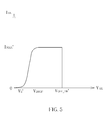
FIGS. 5 and 6 illustrate the operation of the LED lighting device 100, wherein FIG. 5 is a diagram illustrating the current-voltage chart of the two-terminal current controller 120, and FIG. 6 is a diagram illustrating the variations in the related current and voltage when operating the LED lighting device 100. In FIG. 5, the vertical axis represents the current IAK passing through the current limiting unit 120A, and the horizontal axis represents the voltage VAK established across the current limiting unit 120A. In the first embodiment of the present invention, the two-terminal current controller 120 operates in a first mode in which the current limiting unit 120A functions as a voltage-controlled device when 0<VAK<VDROP. In other words, when the voltage VAK exceeds the barrier voltage Vb′ of the two-terminal current controller 120, the current IAK changes with the voltage VAK in a specific manner. The two-terminal current controller 120 operates in a second mode in which the current limiting unit 120A functions as a constant current source when VDROP<VAK<VOFF TH′. In other words, the current IAK is maintained at an adjustable specific current IMAX′ instead of changing with the voltage VAK. The two-terminal current controller 120 functions in a third mode in which the current limiting unit 120A is turned off when VAK>VOFF TH′. In other words, the two-terminal current controller 120 functions as an open-circuited device since the current IAK is suddenly reduced to zero. Meanwhile, the adjusting unit 120B may provide flexible designs with various characteristics by adjusting the value of IMAX′ when the two-terminal current controller 120 operates in the second mode and the value of VOFF TH′ for switching between the second mode and the third mode.
FIG. 6 illustrates the waveforms of the voltage VAK, the current IAK and the current ILED. Since the voltage VAK is associated with the rectified AC voltage VAC whose value varies periodically with time, a cycle between t0-t6 is used for illustration, wherein the period between t0-t3 is the rising period of the rectified AC voltage VAC and the period between t4-t6 is the falling period of the rectified AC voltage VAC. Between t0-t1 when the voltage VAK gradually increases, the current limiting unit 120A of the two-terminal current controller 120 is first turned on, after which the current IAK increases with the voltage VAK in a specific manner and the current ILED is maintained at zero. Between t1-t2 when the voltage VAK is larger than the voltage VDROP, the current limiting unit 120A of the two-terminal current controller 120 is configured to limit the current IAK to a specific current IMAX′, and the current ILED remains zero since the luminescent device 10 is still turned off. Between t2-t4 when the voltage VAK is larger than the voltage VOFF TH′, the current limiting unit 120A of the two-terminal current controller 120 is turned off and the current associated with the rectified AC voltage VAC thus flows through the luminescent device 10. Therefore, the current IAK is reduced to zero, and the current ILED changes with the voltage VAK. Between t4-t5 when the voltage VAK drops to a value between the voltage VDROP and the voltage VOFF TH′, the current limiting unit 120A of the two-terminal current controller 120 is turned on, thereby limiting the current IAK to the specific current IMAX′ and maintaining the current ILED at zero again. Between t5-t6 when the voltage VAK drops below the voltage VDROP, the current IAK decreases with the voltage VAK in a specific manner. In other words, the two-terminal current controller 120 operates in the first mode during t0-t1 and t5-t6 when 0<VAK<VDROP; the two-terminal current controller 120 operates in the second mode during t1-t2 and t4-t5 when VDROP<VAK<VOFF TH′; the two-terminal current controller 120 operates in the third mode during t2-t4 when VAK>VOFF TH′.
FIG. 7 is a diagram of an LED lighting device 200 according to a second embodiment of the present invention. The LED lighting device 200 includes a power supply circuit 110, a two-terminal current controller 120, and a luminescent device 20. Having similar structures, the first and second embodiments of the present invention differ in the luminescent device 20 and how it is connected to the two-terminal current controller 120. In the second embodiment of the present invention, the luminescent device 20 includes two luminescent elements 21 and 25: the luminescent element 21 is coupled in parallel to the two-terminal current controller 120 and includes m light-emitting units D1-Dm coupled in series, wherein ILED AK represents the current flowing through the luminescent element 21 and VAK represents the voltage established across the luminescent element 21; the luminescent element 25 is coupled in series to the two-terminal current controller 120 and includes n light-emitting units D1-Dn coupled in series, wherein ILED represents the current flowing through the luminescent element 25 and VLED represents the voltage established across the luminescent element 25. Each light-emitting unit may include a single light-emitting diode or multiple light-emitting diodes. FIG. 7 depicts the embodiment using a single light-emitting diode. The two-terminal current controller 120 is configured to regulate the current flowing through the luminescent device 20 according to the rectified AC voltage VAC, wherein IAK represents the current flowing through the current limiting unit 120A and VAK represents the voltage established across the current limiting unit 120A. In the second embodiment of the present invention, the barrier voltage Vb′ of the current limiting unit 120A is smaller than the overall barrier voltage m*Vb of the luminescent element 21 (assuming the barrier voltage of each luminescent element is equal to Vb).
FIGS. 8 and 9 illustrate the operation of the LED lighting device 200 according to the second embodiment of the present invention, wherein FIG. 8 is a diagram illustrating the current-voltage chart of the two-terminal current controller 120, and FIG. 9 is a diagram illustrating the variations in the related current and voltage when operating the LED lighting device 200. In FIG. 8, the vertical axis represents the current IAK passing through the current limiting unit 120A, and the horizontal axis represents the voltage VAK established across the two-terminal current controller 120.
During the rising period of the rectified AC voltage VAC, the two-terminal current controller 120 operates in the first mode in which the current limiting unit 120A functions as a voltage-controlled device when 0<VAK<VDROP. In other words, when the voltage VAK exceeds the barrier voltage Vb′ of the two-terminal current controller 120, the current IAK changes with the voltage VAK in a specific manner. The two-terminal current controller 120 operates in the second mode in which the current limiting unit 120A functions as a constant current source when VDROP<VAK<VOFF TH′. In other words, the current IAK is maintained at an adjustable specific current IMAX′ instead of changing with the voltage VAK. The two-terminal current controller 120 operates in the third mode in which the current limiting unit 120A is turned off when VAK>VOFF TH′. In other words, the two-terminal current controller 120 functions as an open-circuited device since the current IAK is suddenly reduced to zero.
During the falling period of the rectified AC voltage VAC, the two-terminal current controller 120 operates in the second mode in which the current limiting unit 120A is turned on for limiting the current IAK to the specific current IMAX′ when VAK<VON TH′. The two-terminal current controller 120 operates in the first mode in which the current limiting unit 120A functions as a voltage-controlled device when 0<VAK<VDROP. In other words, when the voltage VAK exceeds the barrier voltage Vb′ of the two-terminal current controller 120, the current IAK changes with the voltage VAK in a specific manner. Meanwhile, the adjusting unit 120B may provide flexible designs with various characteristics by adjusting the value of IMAX′ when the two-terminal current controller 120 operates in the second mode and the value of VOFF TH′ for switching between the second mode and the third mode.
FIG. 9 illustrates the waveforms of the voltage VAC, VAK, VLED and the current IAK, ILED AK and ILED. Since the rectified AC voltage VAC varies periodically with time, a cycle between t0-t6 is used for illustration, wherein the period between t0-t3 is the rising period of the rectified AC voltage VAC and the period between t4-t6 is the falling period of the rectified AC voltage VAC. Between t0-t1, the voltage VAK established across the two-terminal current controller 120 and the voltage VLED established across the n serially-coupled light-emitting units D1-Dn increase with the rectified AC voltage VAC. Due to smaller barrier voltage, the current limiting unit 120A of the two-terminal current controller 120 is first turned on, after which the current IAK and the current ILED increase with the voltage VAK in a specific manner and the current ILED AK is maintained at zero.
Between t1-t2 when the voltage VAK is larger than the voltage VDROP, the two-terminal current controller 120 is configured to limit the current IAK to the specific current IMAX′, and the current ILED remains zero since the luminescent element 21 is still turned off. With VF representing the forward-bias voltage of each light-emitting unit in the luminescent element 25, the value of the voltage VLED may be represented by m*VF. Therefore, the luminescent element 21 is not conducting between t0-t2, and the rectified AC voltage VAC provided by the power supply circuit 110 is applied to the two-terminal current controller 120 and the n light-emitting units in the luminescent element 25.
Between t2-t4 when the voltage VAK is larger than the voltage VOFF TH′, the two-terminal current controller 120 is turned off and the current associated with the rectified AC voltage VAC thus passes through the luminescent elements 21 and 25. The current IAK is reduced to zero, and the current ILED AK changes with the voltage VAK. Therefore, when the luminescent element 21 is conducting between t2 and t4, the voltage VAK established across the two-terminal current controller 120 is supplied as the luminescent device 20 performs voltage dividing on the rectified AC voltage VAC.
Between t4-t5 when the voltage VAK drops to a value between the voltage VDROP and the voltage VON TH′, the two-terminal current controller 120 is turned on, thereby limiting the current IAK to the specific current IMAX′ and maintaining the current ILED AK at zero again. Between t5-t6 when the voltage VAK drops below the voltage VDROP, the current IAK decreases with the voltage VAK in a specific manner. As depicted in FIGS. 7 and 9, the value of the current ILED is the sum of the current ILED AK and the current IAK. The two-terminal current controller 120 according to the second embodiment of the present invention may increase the effective operational voltage range (such as the output of the rectified AC voltage VAC during t0-t2 and t4-t6), thereby increasing the power factor of the LED luminescence device 200.
FIG. 10 is a diagram of an LED lighting device 300 according to a third embodiment of the present invention. The LED lighting device 300 includes a power supply circuit 110, a plurality of two-terminal current controllers, and a luminescent device 30. Having similar structures, the second and the third embodiments of the present invention differ in that the LED lighting device 300 includes a plurality of two-terminal current controllers (4 two-terminal current controllers 121-124 are depicted in FIG. 10 for illustration) and the luminescent device 30 includes a plurality of luminescent elements (5 luminescent elements 21-24 are depicted in FIG. 10 for illustration). The luminescent elements 21-24 are each coupled in parallel to the corresponding two-terminal current controllers 121-124 and each include a plurality of light-emitting units coupled in series, wherein ILED AK1-ILED AK4 respectively represent the currents flowing through the luminescent elements 21-24 and VAK1-VAK4 respectively represent the voltages established across the luminescent elements 21-24. The luminescent element 25 is coupled in series to the two-terminal current controllers 121-124 and includes a plurality of light-emitting units coupled in series, wherein ILED represents the current flowing through the luminescent element 25 and VLED represents the voltage established across the luminescent element 25. Each light-emitting unit may include a single light-emitting diode or multiple light-emitting diodes. FIG. 10 depicts the embodiment using a single light-emitting diode. In the embodiment illustrated in FIG. 10, the two-terminal current controllers 121-124, each including corresponding current limiting units 121A-124A and corresponding adjusting units 121B-124B, are configured to regulate the currents flowing through the corresponding luminescent devices 21-24 according to the voltages VAK1-VAK4, respectively, wherein IAK1-IAK4 respectively represent the currents flowing through the current limiting units 121A-124A and VAK1-VAK4 respectively represent the voltages established across the current limiting units 121A-124A. In the third embodiment of the present invention, the barrier voltages of the current limiting units 121A-124A are smaller than the overall barrier voltages of the corresponding luminescent elements 21-24.
FIGS. 11A-11D and 12 illustrate the operation of the LED lighting device 300, wherein FIG. 11A-11D are diagrams illustrating the current-voltage charts of the current limiting units 121A-124A, and FIG. 12 is a diagram illustrating the variations in the related current and voltage when operating the LED lighting device 300. The adjusting units 121B-124B may provide flexible designs with various characteristics by adjusting the value of IMAX′ when the two-terminal current controllers 121-124 operate in the second mode and the values of VON TH′ and VOFF TH′ for switching between the second mode and the third mode. In the embodiment illustrated in FIGS. 11A-11D, IMAX1<IMAX2<IMAX3<IMAX4, VON TH1<VON TH2<VON TH3<VON TH4, and VOFF TH1<VOFF TH2<VOFF TH3<VOFF TH4.
FIG. 12 illustrates the waveforms of the voltage VAC and the current ILED when operating the LED lighting device 300. Since the value of the rectified AC voltage VAC varies periodically with time, a cycle between t0-t10 is used for illustration, wherein the period between t0-t5 is the rising period of the rectified AC voltage VAC and the period between t5-t10 is the falling period of the rectified AC voltage VAC.
The operation of the LED lighting device 300 during the rising period t0-t5 is hereby explained. Between t0-t1 when the voltages VAK1-VAK4 increase with the rectified AC voltage VAC, the two-terminal current controllers 121-124 are turned on earlier due to smaller barrier voltages, and the current flows from the power supply circuit 110 to the luminescent element 25 sequentially via the current limiting units 121A-124A (i.e., ILED=TAK1=TAK2=TAK3=TAK4 and ILED AK1=ILED AK2=ILED AK3=ILED AK4=0). Between t1-t2 when the voltage VAK1 is larger than the voltage VOFF TH1, the two-terminal current controller 121 is turned off first, and the current flows from the power supply circuit 110 to the luminescent element 25 sequentially via the luminescent element 21 and the current limiting units 122A-124A (i.e., ILED=ILED AK1=IAK2=IAK3=IAK4 and IAK1=ILED AK2=ILED AK3=ILED AK4=0). Between t2-t3 when the voltage VAK2 is larger than the voltage VOFF TH2, the two-terminal current controller 122 is turned off next, and the current flows from the power supply circuit 110 to the luminescent element 25 sequentially via the luminescent element 21, the luminescent element 22 and the current limiting units 123A-124A (i.e., ILED=ILED AK1=ILED AK2=IAK3=IAK4 and IAK1=IAK2=ILED AK3=ILED AK4=0). Between t3-t4 when the voltage VAK3 is larger than the voltage VOFF TH3, the two-terminal current controller 123 is turned off next, and the current flows from the power supply circuit 110 to the luminescent element 25 sequentially via the luminescent element 21, the luminescent element 22, the luminescent element 23 and the current limiting unit 124A (i.e., ILED=ILED AK1=ILED AK2=ILED AK3=IAK4 and IAK1=IAK2=IAK3=ILED AK4=0). Between t4-t5 when the voltage VAK4 is larger than the voltage VOFF TH4, the two-terminal current controller 124 is turned off next, and the current flows from the power supply circuit 110 to the luminescent element 25 sequentially via the luminescent elements 21-24 (i.e., ILED=ILED AK1=ILED AK2=ILED AK3=ILED AK4 and IAK1=IAK2=IAK3=IAK4=0). During the falling period t5-t10, when the voltages VAK4, VAK3, VAK2 and VAK1 sequentially drop below VON TH4′, VON TH3′, VON TH2′ and VON TH1′, respectively, the current limiting units 124A-121A are sequentially turned on at t6-t9, respectively. The operation of the LED lighting device 300 during the falling period t5-t10 is similar to that during the corresponding rising period t0-t5 as previously illustrated. In other words, during the same period, the luminescent element 25 has the longest conducting time, the luminescent element 21 has the second longest conducting time and the luminescent element 24 has the shortest conducting time. In many applications, the luminescent elements 21-24 may be required to provide different luminescence or become luminescent at different time. The present invention may thus provide flexible designs using the adjusting units 121B-124B.
FIG. 13 is a diagram of an LED lighting device 400 according to a fourth embodiment of the present invention. The LED lighting device 400 includes a power supply circuit 110, a plurality of two-terminal current controllers, and a luminescent device 40. Having similar structure as the third embodiment, the LED lighting device 400 also include a plurality of two-terminal current controllers (5 two-terminal current controllers 121-125 are depicted in FIG. 13 for illustration) and a plurality of luminescent elements (4 luminescent elements 21-24 are depicted in FIG. 10 for illustration), but differ from the LED lighting device 300 in that the two-terminal current controllers 121-124 are each coupled in parallel to the corresponding luminescent elements 21-24 and the two-terminal current controller 125 is coupled in series to the luminescent elements 21-24.
FIG. 14 shows the waveforms of the voltage and the current for illustrating the operation of the LED lighting device 400 according to the fourth embodiment of the present invention. As previously illustrated, the two-terminal current controllers 121-124 are turned off during t4-t5, and the current ILED passing through the luminescent elements 21-24 is determined by the rectified AC voltage VAC provided by the power supply circuit 110. In the third embodiment illustrated in FIGS. 10 and 12, if the power supply circuit 110 fails to provide stable output, the current ILED may exceed the maximum operational current of the luminescent elements 21-25 and thus cause permanent damages to the devices. Therefore, in the LED lighting device 40 according to the fourth embodiment of the present invention, the two-terminal current controller 125 is configured to maintain the current ILED to a specific value IMAX5 which may be adjusted in various applications. The relationship between IMAX1-IMAX5 depicted in FIG. 14 is only for illustrative purpose.
FIG. 15 is a diagram of an LED lighting device 500 according to a fifth embodiment of the present invention. The LED lighting device 500 includes a power supply circuit 410, a two-terminal current controller 120, and a luminescent device 10. Having similar structures, the first and fifth embodiments of the present invention differ in the power supply circuits. In the first embodiment of the present invention, the power supply circuit 110 is configured to rectify the AC voltage VS (such as 110-220V main) using the bridge rectifier 112, thereby providing the rectified AC voltage VAC whose value varies periodically with time. In the fifth embodiment of the present invention, the power supply circuit 410 is configured to receive any AC voltage VS, perform voltage conversion using an AC-AC converter 412, and rectify the converted AC voltage VS using the bridge rectifier 112, thereby providing the rectified AC voltage VAC whose value varies periodically with time. References may be also be made to FIGS. 5 and 6 for illustrating the operation of the LED lighting device 500. Similarly, the second to fourth embodiments of the present invention may also use the power supply circuit 410 for providing the rectified AC voltage VAC.
FIGS. 16 and 17 are diagrams of illustrated embodiments of the two-terminal current controller 120. In these two embodiments, the current limiting unit 120A of the two-terminal current controller 120 includes resistors R1-R7, a switch QN, a comparator CP1, a band-gap reference voltage generator 50, and a voltage-detecting circuit 70. The band-gap reference voltage generator 50 generally adopts devices having positive and negative temperature coefficients in order to achieve temperature-independent output characteristic, thereby providing a stable reference voltage VREF.
The resistor R1 is used for detecting the current flowing through the switch QN, thereby providing a corresponding feedback voltage VFB. The resistors R2-R4 forms a voltage-dividing circuit which provides a reference voltage VREF1 and a reference voltage VREF2 according to the reference voltage VREF. The comparator CP1, having a positive input end for receiving the reference voltage VREF1 and a negative input end for receiving the feedback voltage VFB, is configured to output a control signal Vg to the switch QN according to the relationship between the reference voltage VREF1 and the feedback voltage VFB.
The switch QN may include a field effect transistor (FET), a bipolar junction transistor (BJT) or other devices having similar function. In the embodiments illustrated in FIGS. 14 and 15, an N-type metal-oxide-semiconductor (NMOS) transistor is used for illustration. With the gate coupled to the comparator CP1 for receiving the control signal Vg, the drain-to-source voltage, the gate-to-source voltage and the threshold voltage of the switch QN are represented by VDS, VGS and VTH, respectively. When the switch QN operates in the linear region, its drain current is mainly determined by the drain-to-source voltage VDS; when the switch QN operates in the saturation region, its drain current is only related to the gate-to-source voltage VGS.
During the rising period of the rectified AC voltage VAC, the drain-to-source voltage VDS of the switch QN increases with the voltage VAK. When the voltage VAK does not exceed VDROP, the drain-to-source voltage VDS is smaller than the difference between the gate-to-source voltage VGS and the threshold voltage VTH (VDS<VGS−VTH). The comparator CP1 provides the control signal Vg which allows the switch QN to operate in the linear region where the drain current is mainly determined by the drain-to-source voltage VDS. In other words, the two-terminal current controller 120 is configured to provide the current IAK and voltage VAK whose relationship corresponds to the I-V characteristic of the switch QN when operating in the linear region.
During the rising period of the rectified AC voltage VAC when the VDROP<VAK<VOFF TH′, the drain-to-source voltage VDS is larger than the difference between the gate-to-source voltage VGS and the threshold voltage VTH (VDS>VGS−VTH). The comparator CP1 provides the control signal Vg which results in VGS>VTH, thereby allowing the switch QN to operate in the saturation region. At this time, the drain current of the comparator CP1 is only related to the gate-to-source voltage VGS. In other words, the current IAK does not change with the voltage VAK.
The voltage-detecting circuit 70 includes a logic circuit 72, a voltage edge-detecting circuit 74, and two comparators CP2 and CP3. The comparator CP2, having a positive input end for receiving the reference voltage VREF2 and a negative input end for receiving a voltage VON, is configured to output a control signal VON TH′ according to the relationship between the voltage VON and the reference voltage VREF2. The comparator CP3, having a positive input end for receiving a voltage VOFF and a negative input end for receiving the reference voltage VREF2, is configured to output a control signal VOFF TH′ according to the relationship between the voltage VOFF and the reference voltage VREF2.
The comparator CP2 may determine the relationship between the voltages VAK and VON TH′, while the comparator CP3 may determine the relationship between the voltages VAK and VOFF TH′. Meanwhile, when the voltages VAK is between VOFF TH′ and VON TH′, the voltage edge-detecting circuit 74 is configured to determine whether the rectified AC voltage VAC is during the rising period or during the falling period. Based on the results of the voltage edge-detecting circuit 74 and the comparators CP2 and CP3, the logic circuit 72 outputs a corresponding control signal to the comparator CP1. During the rising period of the rectified AC voltage VAC when the voltage VAK is between VOFF TH′ and VON TH′, the comparator CP1 provides the control signal Vg smaller than the threshold voltage VTH, thereby turning off the switch QN and maintaining the current IAK at zero. During the falling period of the rectified AC voltage VAC when the voltage VAK is between VON TH′ and VOFF TH′, the comparator CP1 provides the control signal Vg larger than the threshold voltage VTH′, thereby operating the switch QN in the saturation region and maintaining the current IAK at IMAX′.
In the embodiment illustrated in FIG. 16, the adjusting unit 120B includes a resistor R8 whose value may be varied for adjusting how the reference voltage VREF is provided to the comparators CP1-CP3 by voltage division. In other words, the values of the reference voltages VREF1 and VREF2 may be adjusted flexibly. As previously illustrated, the comparator CP1 is configured to output the control signal Vg to the switch QN according to the relationship between the reference voltage VREF1 and the feedback voltage VFB, the comparator CP2 is configured to output the control signal VON TH′ according to the relationship between the voltage VON and the reference voltage VREF2, and the comparator CP3 is configured to output the control signal VOFF TH′ according to the relationship between the voltage VOFF and the reference voltage VREF2. Since the drain current of the switch QN is only related to the gate-to-source voltage VGS when operating in the saturation region, the values of the current IMAX′ (when the two-terminal current controller 120 operates in the second mode) and the voltages VON TH′ and VOFF TH′ (for switching between the second and third modes) may be adjusted using the adjusting unit 120B. Therefore, the present invention can provide flexible designs with various characteristics.
In the embodiment illustrated in FIG. 17, the adjusting unit 120B includes resistors R8-R9 and fuses F1-F3. The resistors R8-R9 may be coupled to the resistors R3 and R4 in many ways by laser-burning or current-burning the fuses F1-F3, thereby adjusting the equivalent resistance when performing voltage division. For example, the resistor R8 may be coupled in parallel with the resistor string R3+R4 by burning the fuse F1 alone, the resistor string R8+R9 may be coupled in parallel with the resistor string R3+R4 by burning the fuses F1 and F2 alone, and no extra resistor is coupled in parallel with the resistor string R3+R4 by burning the fuse F3 alone. The present invention may adopt other resistor-fuse configurations, with resistors coupled in series or in parallel, as long as similar results can be achieved. Therefore, the present invention may adjust how the reference voltage VREF is provided to the comparators CP1-CP3 by voltage division. In other words, the values of the reference voltages VREF1 and VREF2 may be adjusted flexibly. As previously illustrated, the comparator CP1 is configured to output the control signal Vg to the switch QN according to the relationship between the reference voltage VREF1 and the feedback voltage VFB, the comparator CP2 is configured to output the control signal VON TH′ according to the relationship between the voltage VON and the reference voltage VREF2, and the comparator CP3 is configured to output the control signal VOFF TH′ according to the relationship between the voltage VOFF and the reference voltage VREF2. Since the drain current of the switch QN is only related to the gate-to-source voltage VGS when operating in the saturation region, the values of the current IMAX′ (when the two-terminal current controller 120 operates in the second mode) and the voltages VON TH′ and VOFF TH′ (for switching between the second and third modes) may be adjusted using the adjusting unit 120B. Therefore, the present invention can provide flexible designs with various characteristics.
In the embodiment illustrated in FIG. 16, the user may adjust the current. In the embodiment illustrated in FIG. 17, manufacturer of the two-terminal current controller may adjust the current for the user. For example, the adjusting unit may be integrated in an IC of the two-terminal current controller. Built-in resistors and laser-burning are well-know to those skilled in the art. FIGS. 15 and 16 are merely for illustrative purpose and do not limit the scope of the present invention.
In the LED lighting devices 100, 200, 300, 400 and 500 of the present invention, the number of the two-terminal current controllers 120-125, the number and configuration of the luminescent elements 21-25, and the type of the power supply circuits 110 and 410 may be determined according to different applications. FIGS. 4, 7, 10 and 12 are merely for illustrative purpose and do not limit the scope of the present invention. Also, the two-terminal current controller 120 depicted in FIG. 16 is an embodiment of the present invention and may be substituted by devices which are able to provide characteristics as shown in FIGS. 5, 6, 8, 9 and 11A-11D.
The LED lighting device of the present invention regulates the current flowing through the serially-coupled light-emitting diodes and controls the number of the turned-on light-emitting diodes using a two-terminal current controller. Some of the light-emitting diodes may be conducted before the rectified AC voltage reaches the overall barrier voltage of all light-emitting diodes for improving the power factor. Therefore, the present invention may provide lighting devices having large effective operational voltage range and high brightness.
Those skilled in the art will readily observe that numerous modifications and alterations of the device and method may be made while retaining the teachings of the invention.

Claims (28)

What is claimed is:
1. A light-emitting diode (LED) lighting device, comprising:
a luminescent device configured to provide light according to a first current;
a two-terminal current controller coupled in parallel with the luminescent device and configured to regulate the first current according to a voltage established across the luminescent device, wherein:
during a rising period of a rectified alternative-current (AC) voltage when the voltage established across the luminescent device does not exceed a first voltage, the two-terminal current controller operates in a first mode;
during the rising period when the voltage established across the luminescent device exceeds the first voltage but does not exceed a second voltage, the two-terminal current controller operates in a second mode;
during the rising period when the voltage established across the luminescent device exceeds the second voltage, the two-terminal current controller operates in a third mode; and
the two-terminal current controller includes:
a current limiting unit configured to:
conduct a second current associated with the rectified AC voltage, regulate the second current according to the voltage established across the luminescent device and maintain the first current at zero when the two-terminal current controller operates in the first mode;
conduct the second current, maintain the second current at a first predetermined value larger than zero and maintain the first current at zero when the two-terminal current controller operates in the second mode; and
switch off when the two-terminal current controller operates in the third mode; and
an adjusting unit configured to adjust the first predetermined value and the second voltage.
2. The LED lighting device of claim 1, wherein during a falling period of the rectified AC voltage when the voltage established across the luminescent device is between the first voltage and a third voltage larger than the second voltage, the two-terminal current controller operates in the second mode in which the current limiting unit is configured to conduct the second current, maintain the second current at the first predetermined value and maintain the first current at zero.
3. The LED lighting device of claim 2, wherein the current limiting unit comprises:
a switch configured to conduct the second current according to a control signal;
a band-gap reference voltage generator configured to provide a band-gap reference voltage;
a first voltage-dividing circuit configured to provide a first reference voltage and a second reference voltage by voltage-dividing the band-gap reference voltage;
a second voltage-dividing circuit configured to provide a fourth voltage and a fifth voltage by voltage-dividing the rectified AC voltage;
a current-detecting circuit coupled in series to the switch and configured to detect the second current and provide a corresponding feedback voltage;
a voltage edge-detecting circuit configured to determine whether the rectified AC voltage is during the rising period or the falling period;
a first comparator configured to provide the control signal according to a relationship between the first reference voltage and the feedback voltage, the second voltage, the third voltage and a determining result of the voltage edge-detecting circuit;
a second comparator configured to provide the second voltage according to a relationship between the second reference voltage and the fourth voltage; and
a third comparator configured to provide the third voltage according to a relationship between the second reference voltage and the fifth voltage.
4. The LED lighting device of claim 3, wherein the adjusting unit includes:
a resistor coupled in parallel with the first voltage-dividing circuit for adjusting the first reference voltage and the second reference voltage.
5. The LED lighting device of claim 3, wherein the adjusting unit includes:
a resistor; and
a fuse coupled in parallel with the resistor for coupling the resistor in parallel with the first voltage-dividing circuit when burned, thereby adjusting the first reference voltage and the second reference voltage.
6. The LED lighting device of claim 3, wherein the adjusting unit includes:
a resistor; and
a fuse coupled in series to the resistor for coupling the resistor in parallel with the first voltage-dividing circuit when unburned, thereby adjusting the first reference voltage and the second reference voltage.
7. The LED lighting device of claim 3, wherein:
during the falling period when the voltage established across the luminescent device does not exceed the first voltage, the switch is configured to regulate the second current according to the control signal; and
during the falling period when the voltage established across the luminescent device exceeds the first voltage but does not exceed the third voltage, the switch is configured to maintain the second current at the first predetermined value according to the control signal and maintain the first current at zero.
8. The LED lighting device of claim 7, wherein the two-terminal current controller is configured to regulate the second current according to the voltage established across the luminescent device, so that a relationship between the voltage established across the luminescent device and the second current matches a characteristic when the switch operates in a specific operational region.
9. The LED lighting device of claim 1, wherein the current limiting unit comprises:
a switch configured to conduct the second current according to a control signal;
a band-gap reference voltage generator configured to provide a band-gap reference voltage;
a first voltage-dividing circuit configured to provide a first reference voltage and a second reference voltage by voltage-dividing the band-gap reference voltage;
a second voltage-dividing circuit configured to provide a fourth voltage and a fifth voltage by voltage-dividing the rectified AC voltage;
a current-detecting circuit coupled in series to the switch and configured to detect the second current and provide a corresponding feedback voltage;
a voltage edge-detecting circuit configured to determine whether the rectified AC voltage is during the rising period or the falling period;
a first comparator configured to provide the control signal according to a relationship between the first reference voltage and the feedback voltage, the second voltage, the third voltage and a determining result of the voltage edge-detecting circuit; and
a second comparator configured to provide the second voltage according to a relationship between the second reference voltage and the fourth voltage.
10. The LED lighting device of claim 9, wherein the adjusting unit includes:
a resistor coupled in parallel with the first voltage-dividing circuit for adjusting the first reference voltage and the second reference voltage.
11. The LED lighting device of claim 9, wherein the adjusting unit includes:
a resistor; and
a fuse coupled in parallel with the resistor for coupling the resistor in parallel with the first voltage-dividing circuit when burned and bypassing the resistor when unburned, thereby adjusting the first reference voltage and the second reference voltage.
12. The LED lighting device of claim 9, wherein the adjusting unit includes:
a resistor; and
a fuse coupled in series to the resistor for coupling the resistor in parallel with the first voltage-dividing circuit when unburned, thereby adjusting the first reference voltage and the second reference voltage.
13. The LED lighting device of claim 9, wherein:
during the rising period when the voltage established across the luminescent device does not exceed the first voltage, the switch is configured to regulate the second current according to the control signal; and
during the rising period when the voltage established across the luminescent device exceeds the first voltage, the switch is configured to maintain the second current at the first predetermined value according to the control signal.
14. The LED lighting device of claim 1, wherein a barrier voltage for turning on the two-terminal current controller is smaller than a barrier voltage for turning on the luminescent device.
15. The LED lighting device of claim 1, further comprising:
n luminescent devices coupled in series and each configured to provide light according to a corresponding first current; and
n two-terminal current controllers, each corresponding two-terminal current controller coupled in parallel with a corresponding luminescent device among the n luminescent devices and configured to regulate the corresponding first current according to a voltage established across the corresponding luminescent device, wherein:
during the rising period when the voltage established across the corresponding luminescent device does not exceed the first voltage, the corresponding two-terminal current controller operates in the first mode;
during the rising period when the voltage established across the corresponding luminescent device exceeds the first voltage but does not exceed the second voltage, the corresponding two-terminal current controller operates in the second mode; and
during the rising period when the voltage established across the corresponding luminescent device exceeds the second voltage, the corresponding two-terminal current controller operates in the third mode.
16. The LED lighting device of claim 15, further comprising:
an (n+1)th two-terminal current controller coupled in series to the n luminescent devices and comprising:
an (n+1)th current limiting unit configured to maintain the first current at a second predetermined value larger than zero when the n two-terminal current controllers are turned off; and
an (n+1)th adjusting unit configured to adjust the second predetermined value.
17. A two-terminal current controller for controlling a first current passing through a load, wherein:
during a rising period of a rectified AC voltage when a voltage established across the load does not exceed a first voltage, the two-terminal current controller operates in a first mode;
during the rising period when the voltage established across the load exceeds the first voltage but does not exceed a second voltage, the two-terminal current controller operates in a second mode; and
during the rising period when the voltage established across the load exceeds the second voltage, the two-terminal current controller operates in a third mode; and
the two-terminal current controller includes:
a current limiting unit configured to:
conduct a second current associated with the rectified AC voltage, regulate the second current according to the voltage established across the load and maintain the first current at zero when the two-terminal current controller operates in the first mode;
conduct the second current, maintain the second current at a predetermined value larger than zero and maintain the first current at zero when the two-terminal current controller operates in the second mode; and
switch off when the two-terminal current controller operates in the third mode; and
an adjusting unit configured to adjust the predetermined value and the second voltage.
18. The two-terminal current controller of claim 17, wherein during a falling period of the rectified AC voltage when the voltage established across the load is between the first voltage and a third voltage larger than the second voltage, the two-terminal current controller operates in the second mode in which the current limiting unit is configured to conduct the second current, maintain the second current at the predetermined value and maintain the first current at zero.
19. The two-terminal current controller of claim 18, wherein the current limiting unit comprises:
a switch configured to conduct the second current according to a control signal;
a band-gap reference voltage generator configured to provide a band-gap reference voltage;
a first voltage-dividing circuit configured to provide a first reference voltage and a second reference voltage by voltage-dividing the band-gap reference voltage;
a second voltage-dividing circuit configured to provide a fourth voltage and a fifth voltage by voltage-dividing the rectified AC voltage;
a current-detecting circuit coupled in series to the switch and configured to detect the second current and provide a corresponding feedback voltage;
a voltage edge-detecting circuit configured to determine whether the rectified AC voltage is during the rising period or the falling period;
a first comparator configured to provide the control signal according to a relationship between the first reference voltage and the feedback voltage, the second voltage, the third voltage and a determining result of the voltage edge-detecting circuit;
a second comparator configured to provide the second voltage according to a relationship between the second reference voltage and the fourth voltage; and
a third comparator configured to provide the third voltage according to a relationship between the second reference voltage and the fifth voltage.
20. The two-terminal current controller of claim 19, wherein the adjusting unit includes:
a resistor; and
a fuse coupled in parallel with the resistor for coupling the resistor in parallel with the first voltage-dividing circuit when burned, thereby adjusting the first reference voltage and the second reference voltage.
21. The two-terminal current controller of claim 19, wherein the adjusting unit includes:
a resistor; and
a fuse coupled in series to the resistor for coupling the resistor in parallel with the first voltage-dividing circuit when unburned, thereby adjusting the first reference voltage and the second reference voltage.
22. The two-terminal current controller of claim 19, wherein:
during the falling period when the voltage established across the load does not exceed the first voltage, the switch is configured to regulate the second current according to the control signal; and
during the falling period when the voltage established across the load exceeds the first voltage but does not exceed the third voltage, the switch is configured to maintain the second current at the predetermined value according to the control signal and maintain the first current at zero.
23. The two-terminal current controller of claim 22, wherein the two-terminal current controller is configured to regulate the second current according to the voltage established across the load, so that a relationship between the voltage established across the load and the second current matches a characteristic when the switch operates in a specific operational region.
24. The two-terminal current controller of claim 17, wherein the current limiting unit comprises:
a switch configured to conduct the second current according to a control signal;
a band-gap reference voltage generator configured to provide a band-gap reference voltage;
a first voltage-dividing circuit configured to provide a first reference voltage and a second reference voltage by voltage-dividing the band-gap reference voltage;
a second voltage-dividing circuit configured to provide a fourth voltage and a fifth voltage by voltage-dividing the rectified AC voltage;
a current-detecting circuit coupled in series to the switch and configured to detect the second current and provide a corresponding feedback voltage;
a voltage edge-detecting circuit configured to determine whether the rectified AC voltage is during the rising period or the falling period;
a first comparator configured to provide the control signal according to a relationship between the first reference voltage and the feedback voltage, the second voltage, the third voltage and a determining result of the voltage edge-detecting circuit; and
a second comparator configured to provide the second voltage according to a relationship between the second reference voltage and the fourth voltage.
25. The two-terminal current controller of claim 24, wherein the adjusting unit includes:
a resistor; and
a fuse coupled in parallel with the resistor for coupling the resistor in parallel with the first voltage-dividing circuit when burned and bypassing the resistor when unburned, thereby adjusting the first reference voltage and the second reference voltage.
26. The two-terminal current controller of claim 24, wherein the adjusting unit includes:
a resistor; and
a fuse coupled in series to the resistor for coupling the resistor in parallel with the first voltage-dividing circuit when unburned, thereby adjusting the first reference voltage and the second reference voltage.
27. The two-terminal current controller of claim 24, wherein:
during the rising period when the voltage established across the load does not exceed the first voltage, the switch is configured to regulate the second current according to the control signal; and
during the rising period when the voltage established across the load exceeds the first voltage, the switch is configured to maintain the second current at the predetermined value according to the control signal.
28. The two-terminal current controller of claim 17, wherein a barrier voltage for turning on the two-terminal current controller is smaller than a barrier voltage for turning on the load.
US13/052,132 2010-12-07 2011-03-21 Two-terminal current controller and related LED lighting device Active 2031-12-20 US8638043B2 (en)

Priority Applications (1)

Application Number Priority Date Filing Date Title
US13/743,345 US8638047B2 (en) 2010-12-07 2013-01-17 Two-terminal current controller and related LED lighting device

Applications Claiming Priority (3)

Application Number Priority Date Filing Date Title
TW099142624 2010-12-07
TW99142624A 2010-12-07
TW099142624A TWI435654B (en) 2010-12-07 2010-12-07 Two-terminal current controller and related led lighting device

Related Child Applications (1)

Application Number Title Priority Date Filing Date
US13/743,345 Continuation-In-Part US8638047B2 (en) 2010-12-07 2013-01-17 Two-terminal current controller and related LED lighting device

Publications (2)

Publication Number Publication Date
US20120139448A1 US20120139448A1 (en) 2012-06-07
US8638043B2 true US8638043B2 (en) 2014-01-28

Family

ID=46161585

Family Applications (1)

Application Number Title Priority Date Filing Date
US13/052,132 Active 2031-12-20 US8638043B2 (en) 2010-12-07 2011-03-21 Two-terminal current controller and related LED lighting device

Country Status (3)

Country Link
US (1) US8638043B2 (en)
CN (1) CN102563400B (en)
TW (1) TWI435654B (en)

Cited By (6)

* Cited by examiner, † Cited by third party
Publication number Priority date Publication date Assignee Title
US20130257282A1 (en) * 2012-03-29 2013-10-03 Nxp B.V. Led driver and a method of driving leds
US20140197741A1 (en) * 2011-07-15 2014-07-17 Citizen Electronics Co., Ltd. Led lighting apparatus
US20150110141A1 (en) * 2012-06-20 2015-04-23 Wisdom Technologies Holding Limited Driving circuit and illumination device having light-emitting elements
US20150334801A1 (en) * 2014-05-16 2015-11-19 Unity Opto Technology Co., Ltd. Purely resistive dimming circuit
US9686833B2 (en) 2015-06-26 2017-06-20 Samsung Electronics Co., Ltd. LED driving apparatus and lighting apparatus including the same
US10807516B2 (en) * 2016-09-09 2020-10-20 Koito Manufacturing Co., Ltd. Lighting circuit

Families Citing this family (34)

* Cited by examiner, † Cited by third party
Publication number Priority date Publication date Assignee Title
US8674609B2 (en) 2010-04-15 2014-03-18 Iml International Two-terminal current controller and related LED lighting device
TWI425862B (en) * 2010-04-15 2014-02-01 安恩國際公司 Two-terminal current controller and related led lighting device
US8547025B2 (en) 2010-04-15 2013-10-01 Iml International Two-terminal current controller and related LED lighting device
US8890433B2 (en) 2010-04-15 2014-11-18 Iml International Two-terminal current controller and related LED lighting device
US20130069546A1 (en) * 2010-11-23 2013-03-21 O2Micro, Inc. Circuits and methods for driving light sources
US9030121B2 (en) * 2010-11-23 2015-05-12 O2Micro, Inc. Circuits and methods for driving light sources
US8564219B2 (en) * 2010-11-23 2013-10-22 O2Micro, Inc. Circuits and methods for driving light sources
DE112012005774T5 (en) * 2012-06-15 2014-10-30 Vastview Technology Inc. Method and device for segmenting and driving LED-based lighting units
TW201408131A (en) * 2012-08-08 2014-02-16 安恩國際公司 Two-terminal current controller and related LED lighting device
WO2014057373A2 (en) * 2012-10-08 2014-04-17 Koninklijke Philips N.V. Methods and apparatus for compensating a removal of leds from an led array
TW201431432A (en) * 2013-01-17 2014-08-01 安恩國際公司 Two-terminal current controller and related LED lighting device
CN103974505B (en) * 2013-02-06 2016-05-04 安恩国际公司 Light emitting diode illuminating apparatus
US9013109B2 (en) * 2013-02-06 2015-04-21 Iml International Light-emitting diode lighting device with adjustable current settings and switch voltages
WO2014126258A1 (en) * 2013-02-18 2014-08-21 シチズンホールディングス株式会社 Led drive circuit
JP6155703B2 (en) * 2013-03-04 2017-07-05 セイコーエプソン株式会社 Light source device and projector
US9113523B2 (en) * 2013-05-15 2015-08-18 Iml International Light-emitting diode lighting device having multiple driving stages
TWI569683B (en) * 2013-05-24 2017-02-01 Vastview Tech Inc A device for driving a high voltage light emitting diode string
US9226354B2 (en) * 2013-06-03 2015-12-29 Iml International Light-emitting diode lighting device having multiple driving stages
CN104244503B (en) * 2013-06-18 2017-03-22 钰瀚科技股份有限公司 Device for driving light-emitting diode string with high-voltage applied
CN104284478A (en) * 2013-07-10 2015-01-14 安恩科技股份有限公司 Light-emitting diode lighting device having multiple driving stages
JP6242654B2 (en) 2013-10-23 2017-12-06 東芝テック株式会社 Power converter
CN104753104A (en) * 2013-12-30 2015-07-01 鸿富锦精密工业(武汉)有限公司 USB charging circuit with current regulating function
US20150201471A1 (en) * 2014-01-16 2015-07-16 Iml International Low-flicker light-emitting diode lighting device having multiple driving stages
FR3018659B1 (en) * 2014-03-14 2020-03-27 Koito Manufacturing Co., Ltd. VEHICLE LAMP AND VEHICLE LAMP CONTROL DEVICE
FR3023119B1 (en) * 2014-06-30 2019-08-02 Aledia OPTOELECTRONIC CIRCUIT WITH ELECTROLUMINESCENT DIODES
US9351363B1 (en) * 2014-11-20 2016-05-24 Iml International Dual mode operation light-emitting diode lighting device having multiple driving stages
WO2016163533A1 (en) * 2015-04-08 2016-10-13 シチズンホールディングス株式会社 Led drive circuit
JP6511322B2 (en) * 2015-04-14 2019-05-15 新日本無線株式会社 LED drive circuit
TWM515620U (en) * 2015-09-11 2016-01-11 Luxmill Electronic Co Ltd Multi-level LED driving circuit for eliminating undershoot
JP6720753B2 (en) 2016-07-27 2020-07-08 東芝ライテック株式会社 Vehicle lighting device and vehicle lamp
US9794992B1 (en) * 2016-07-27 2017-10-17 Vastview Technology Inc. Universal method for driving LEDs using high voltage
CN106524089B (en) * 2016-12-21 2023-06-13 广西水利电力职业技术学院 Control system of liftable lamp stand
JP6922578B2 (en) * 2017-09-13 2021-08-18 東芝ライテック株式会社 Vehicle lighting and vehicle lighting
CN112770444B (en) * 2021-01-29 2023-03-14 漳州立达信光电子科技有限公司 Full-cycle load driving system

Citations (19)

* Cited by examiner, † Cited by third party
Publication number Priority date Publication date Assignee Title
JP2006244848A (en) 2005-03-03 2006-09-14 Jamco Corp Illumination-purpose light-emitting diode driving circuit
US20060267514A1 (en) 2003-05-07 2006-11-30 Koninklijke Philips Electronics N.V. Current control method and circuit for light emitting diodes
US20080001547A1 (en) 2005-09-20 2008-01-03 Negru Sorin L Driving parallel strings of series connected LEDs
JP2008059811A (en) 2006-08-29 2008-03-13 Avago Technologies Ecbu Ip (Singapore) Pte Ltd Device and method for driving led
JP2008130377A (en) 2006-11-21 2008-06-05 Matsushita Electric Works Ltd Led lighting circuit and illumination fixture using it
TW200850048A (en) 2007-05-01 2008-12-16 Pacific Tech Microelectronics Inc LED current control circuits and methods
JP2009134933A (en) 2007-11-29 2009-06-18 Mitsubishi Electric Corp Led lighting device, and headlight for vehicle
WO2009153696A1 (en) 2008-06-17 2009-12-23 Philips Intellectual Property & Standards Gmbh Harmonic compensation circuit and method for an led light unit
US20090322235A1 (en) 2008-06-30 2009-12-31 Shian-Sung Shiu Led driving circuit, led driving control unit and transistor switch module thereof
TW201004471A (en) 2008-07-01 2010-01-16 Delta Electronics Inc Current supply circuit and current control circuit for LED
KR20110023551A (en) 2009-08-31 2011-03-08 삼성전기주식회사 Led driving circuit
JP2011065922A (en) 2009-09-18 2011-03-31 Toshiba Lighting & Technology Corp Led lighting device and illumination device
WO2011058805A1 (en) 2009-11-13 2011-05-19 日亜化学工業株式会社 Light-emitting diode drive device and light-emitting diode illumination control method
TW201136443A (en) 2010-04-15 2011-10-16 Addtek Corp Two-terminal current controller and related LED lighting device
US20110273112A1 (en) 2010-05-07 2011-11-10 Samsung Electro-Mechanics Co., Ltd. Light emitting driver
US20110279044A1 (en) * 2008-04-10 2011-11-17 Fu-Hwa Maiw High efficiency power drive device enabling serial connection of light emitting diode lamps thereto
KR101132194B1 (en) 2011-10-18 2012-04-06 삼성엘이디 주식회사 Light emitting apparatus and led driving method using the same
US8299724B2 (en) * 2010-03-19 2012-10-30 Active-Semi, Inc. AC LED lamp involving an LED string having separately shortable sections
WO2013011924A1 (en) 2011-07-15 2013-01-24 シチズンホールディングス株式会社 Led illumination device

Family Cites Families (3)

* Cited by examiner, † Cited by third party
Publication number Priority date Publication date Assignee Title
DE69914266T2 (en) * 1998-08-18 2004-11-18 Koninklijke Philips Electronics N.V. Controlled power source with accelerated switching
US7265952B2 (en) * 2005-06-09 2007-09-04 Addtek Corp. Two-terminal protecting circuit
JP4762722B2 (en) * 2006-01-10 2011-08-31 ローム株式会社 Power supply device and electronic apparatus equipped with the same

Patent Citations (22)

* Cited by examiner, † Cited by third party
Publication number Priority date Publication date Assignee Title
US20060267514A1 (en) 2003-05-07 2006-11-30 Koninklijke Philips Electronics N.V. Current control method and circuit for light emitting diodes
JP2006244848A (en) 2005-03-03 2006-09-14 Jamco Corp Illumination-purpose light-emitting diode driving circuit
US20080001547A1 (en) 2005-09-20 2008-01-03 Negru Sorin L Driving parallel strings of series connected LEDs
JP2008059811A (en) 2006-08-29 2008-03-13 Avago Technologies Ecbu Ip (Singapore) Pte Ltd Device and method for driving led
JP2008130377A (en) 2006-11-21 2008-06-05 Matsushita Electric Works Ltd Led lighting circuit and illumination fixture using it
US7683553B2 (en) 2007-05-01 2010-03-23 Pacifictech Microelectronics, Inc. LED current control circuits and methods
TW200850048A (en) 2007-05-01 2008-12-16 Pacific Tech Microelectronics Inc LED current control circuits and methods
JP2009134933A (en) 2007-11-29 2009-06-18 Mitsubishi Electric Corp Led lighting device, and headlight for vehicle
US20110279044A1 (en) * 2008-04-10 2011-11-17 Fu-Hwa Maiw High efficiency power drive device enabling serial connection of light emitting diode lamps thereto
JP2011524621A (en) 2008-06-17 2011-09-01 コーニンクレッカ フィリップス エレクトロニクス エヌ ヴィ Harmonic compensation circuit and method for LED lighting unit
WO2009153696A1 (en) 2008-06-17 2009-12-23 Philips Intellectual Property & Standards Gmbh Harmonic compensation circuit and method for an led light unit
US20090322235A1 (en) 2008-06-30 2009-12-31 Shian-Sung Shiu Led driving circuit, led driving control unit and transistor switch module thereof
TW201004471A (en) 2008-07-01 2010-01-16 Delta Electronics Inc Current supply circuit and current control circuit for LED
US8183795B2 (en) 2008-07-01 2012-05-22 Delta Electronics, Inc. LED current-supplying circuit and LED current-controlling circuit
KR20110023551A (en) 2009-08-31 2011-03-08 삼성전기주식회사 Led driving circuit
JP2011065922A (en) 2009-09-18 2011-03-31 Toshiba Lighting & Technology Corp Led lighting device and illumination device
WO2011058805A1 (en) 2009-11-13 2011-05-19 日亜化学工業株式会社 Light-emitting diode drive device and light-emitting diode illumination control method
US8299724B2 (en) * 2010-03-19 2012-10-30 Active-Semi, Inc. AC LED lamp involving an LED string having separately shortable sections
TW201136443A (en) 2010-04-15 2011-10-16 Addtek Corp Two-terminal current controller and related LED lighting device
US20110273112A1 (en) 2010-05-07 2011-11-10 Samsung Electro-Mechanics Co., Ltd. Light emitting driver
WO2013011924A1 (en) 2011-07-15 2013-01-24 シチズンホールディングス株式会社 Led illumination device
KR101132194B1 (en) 2011-10-18 2012-04-06 삼성엘이디 주식회사 Light emitting apparatus and led driving method using the same

Non-Patent Citations (1)

* Cited by examiner, † Cited by third party
Title
U.S. Appl. No. 13/743,345, filed Jan. 17, 2013. *

Cited By (9)

* Cited by examiner, † Cited by third party
Publication number Priority date Publication date Assignee Title
US20140197741A1 (en) * 2011-07-15 2014-07-17 Citizen Electronics Co., Ltd. Led lighting apparatus
US9485830B2 (en) * 2011-07-15 2016-11-01 Citizen Holdings Co., Ltd. LED lighting apparatus
US20130257282A1 (en) * 2012-03-29 2013-10-03 Nxp B.V. Led driver and a method of driving leds
US20150110141A1 (en) * 2012-06-20 2015-04-23 Wisdom Technologies Holding Limited Driving circuit and illumination device having light-emitting elements
US9271357B2 (en) * 2012-06-20 2016-02-23 Wisdom Technologies Holding Limited Driving circuit and illumination device having light-emitting elements
US20150334801A1 (en) * 2014-05-16 2015-11-19 Unity Opto Technology Co., Ltd. Purely resistive dimming circuit
US9485824B2 (en) * 2014-05-16 2016-11-01 Unity Opto Technology Co., Ltd. Purely resistive dimming circuit
US9686833B2 (en) 2015-06-26 2017-06-20 Samsung Electronics Co., Ltd. LED driving apparatus and lighting apparatus including the same
US10807516B2 (en) * 2016-09-09 2020-10-20 Koito Manufacturing Co., Ltd. Lighting circuit

Also Published As

Publication number Publication date
US20120139448A1 (en) 2012-06-07
TW201225738A (en) 2012-06-16
CN102563400B (en) 2013-12-18
CN102563400A (en) 2012-07-11
TWI435654B (en) 2014-04-21

Similar Documents

Publication Publication Date Title
US8638043B2 (en) Two-terminal current controller and related LED lighting device
US8638047B2 (en) Two-terminal current controller and related LED lighting device
US8319443B2 (en) Two-terminal current controller and related LED lighting device
US8339049B2 (en) LED driving circuit having a large operational range in voltage
TWI477190B (en) Light emitting diode driving apparatus
KR101582500B1 (en) Light-emitting diode lighting device with adjustable current settings and switch voltages
KR20140107838A (en) Circuit to control led lighting apparatus
US8547025B2 (en) Two-terminal current controller and related LED lighting device
TW201431432A (en) Two-terminal current controller and related LED lighting device
US8847501B1 (en) Apparatus for driving LEDs using high voltage
TW201531154A (en) Low-flicker light-emitting diode lighting device having multiple driving stages
TWI519204B (en) Light-emitting diode lighting device having multiple driving stages
KR20160070925A (en) Circuit to control led lighting apparatus
US9113523B2 (en) Light-emitting diode lighting device having multiple driving stages
US8674609B2 (en) Two-terminal current controller and related LED lighting device
KR101408027B1 (en) Two-terminal current controller and related led lighting device
US8890433B2 (en) Two-terminal current controller and related LED lighting device
JP5739834B2 (en) LED lighting device and two-terminal current controller
TW201408131A (en) Two-terminal current controller and related LED lighting device
KR20190045818A (en) Light-emitting diode lighting device
TWI637655B (en) Low-flicker light-emitting diode lighting device
US9226354B2 (en) Light-emitting diode lighting device having multiple driving stages

Legal Events

Date Code Title Description
AS Assignment

Owner name: ADDTEK CORP., TAIWAN

Free format text: ASSIGNMENT OF ASSIGNORS INTEREST;ASSIGNORS:CHIANG, YUNG-HSIN;LI, YI-MEI;REEL/FRAME:025986/0914

Effective date: 20110216

AS Assignment

Owner name: IML INTERNATIONAL, CAYMAN ISLANDS

Free format text: ASSIGNMENT OF ASSIGNORS INTEREST;ASSIGNOR:ADDTEK CORP;REEL/FRAME:027595/0153

Effective date: 20120118

STCF Information on status: patent grant

Free format text: PATENTED CASE

FPAY Fee payment

Year of fee payment: 4

AS Assignment

Owner name: IML HONG KONG LIMITED, HONG KONG

Free format text: ASSIGNMENT OF ASSIGNORS INTEREST;ASSIGNOR:IML INTERNATIONAL;REEL/FRAME:056321/0926

Effective date: 20210511

MAFP Maintenance fee payment

Free format text: PAYMENT OF MAINTENANCE FEE, 8TH YR, SMALL ENTITY (ORIGINAL EVENT CODE: M2552); ENTITY STATUS OF PATENT OWNER: SMALL ENTITY

Year of fee payment: 8