US8634004B2 - Monitoring of optical defects in an image capture system - Google Patents
Monitoring of optical defects in an image capture system Download PDFInfo
- Publication number
- US8634004B2 US8634004B2 US13/144,293 US201013144293A US8634004B2 US 8634004 B2 US8634004 B2 US 8634004B2 US 201013144293 A US201013144293 A US 201013144293A US 8634004 B2 US8634004 B2 US 8634004B2
- Authority
- US
- United States
- Prior art keywords
- sensor
- responses
- photosensitive elements
- image capture
- region
- Prior art date
- Legal status (The legal status is an assumption and is not a legal conclusion. Google has not performed a legal analysis and makes no representation as to the accuracy of the status listed.)
- Expired - Fee Related, expires
Links
Images


Classifications
-
- H—ELECTRICITY
- H04—ELECTRIC COMMUNICATION TECHNIQUE
- H04N—PICTORIAL COMMUNICATION, e.g. TELEVISION
- H04N17/00—Diagnosis, testing or measuring for television systems or their details
- H04N17/002—Diagnosis, testing or measuring for television systems or their details for television cameras
-
- H—ELECTRICITY
- H04—ELECTRIC COMMUNICATION TECHNIQUE
- H04N—PICTORIAL COMMUNICATION, e.g. TELEVISION
- H04N23/00—Cameras or camera modules comprising electronic image sensors; Control thereof
- H04N23/80—Camera processing pipelines; Components thereof
- H04N23/81—Camera processing pipelines; Components thereof for suppressing or minimising disturbance in the image signal generation
Definitions
- This invention relates to the field of digital image capture systems.
- Such an image capture system may, for example, be a module suitable for use in a digital camera, a reflex camera, a scanner, a fax, an endoscope, a movie camera, a camcorder, a surveillance camera, a toy, a camera integrated or connected to a telephone or a personal digital assistant or a computer, a thermal camera, an ultrasonography system, an MRI (magnetic resonance imaging) device, an x-ray radiography device, etc.
- MRI magnetic resonance imaging
- Such a system conventionally comprises a sensor including a plurality of photosensitive elements (for example pixels) which convert a quantity of received light into digital values, and an optical device comprising one or more lenses for focusing the light on the sensor. These two elements together are commonly referred to as an “optical sensor module”.
- the sensor may, for example, be a CCD (charge-coupled device), CMOS (Complementary Metal-Oxide Semiconductor), CID (Charge Injection Device), IRCCD (Infrared CCD), ICCD (Intensified CCD), EBCCD (Electron Bombarded CCD), MIS (Metal Insulator Semiconductor), APS (Active Pixel Sensor), QWIP (Quantum Well Infrared Photodetector), MQW (Multi-Quantum Well), or other device. It may possibly be associated with a Bayer filter in order to obtain a color image.
- CCD charge-coupled device
- CMOS Complementary Metal-Oxide Semiconductor
- CID Charge Injection Device
- IRCCD Infrared CCD
- ICCD Intensified CCD
- EBCCD Electrodeted CCD
- MIS Metal Insulator Semiconductor
- APS Active Pixel Sensor
- QWIP Quadantum Well Infrared
- a lens assembly step is necessary for each optical sensor module, in which the sensor is positioned relative to its associated optical device. Ideally, these two elements must be centered relative to each other and be in parallel planes, to enable the module to provide the best possible rendering of the image. In reality, the sensor and the optical device may not be optimally positioned during this assembly step.
- FIGS. 1A-1C show examples of a first positioning defect due to a tilt defect in an optical sensor module.
- the optical sensor module presented in these figures comprises an optical device L and a sensor C as indicated above.
- a housing B receives the sensor C and has a lens support H (commonly referred to as the Holder) which serves to position the optical device L relative to the housing B, by a screw thread for example.
- the different elements of the optical sensor module are correctly assembled.
- the sensor C and the optical device L are parallel to each other, which represents proper lens assembly.
- FIG. 1B illustrates a first example of a defect in the relative tilt between a sensor C and an optical device L.
- the sensor C is assembled at an angle in the housing B of the module. This causes an asymmetrical change in the clarity of the image provided by the sensor C. This is referred to as sensor tilt.
- FIG. 1C illustrates another example of a defect in the relative angle between a sensor C and an optical device L.
- the optical holder H which is angled, which results in the non-parallelism of the optical device and the sensor C.
- Such a defect in the verticality of the optical holder H can be called holder tilt. This also causes an asymmetrical change in the clarity of the image provided by the sensor C.
- tilt defects may appear separately or together.
- the direct result of such relative tilt consists of a phenomenon of asymmetrical blurring in the image.
- This constitutes a lens defect and processed needs to be applied in order to obtain a sharp image.
- the image evolves from blurred to sharp in the direction of the tilt defect.
- the blurring is said to be asymmetrical because the distance between the sensor and the lens is different on the right and on the left, corresponding to a variable focus for the image.
- the right portion of the provided image will be sharp while the left portion of the image will be blurred.
- FIGS. 2A-2D Another type of defect that an optical-sensor module may have is a relative decentering defect, illustrated by FIGS. 2A-2D .
- FIG. 2A shows the optical sensor module of an image capture system, comprising a circular optical device L having a center O L , projecting the light it receives onto a sensor C in a circular lighting area I centered around O L .
- the present sensor C has a central region Z comprising a certain number of pixels dedicated to capturing images, surrounded by a peripheral region P.
- the optical device L is perfectly centered with this central region Z, meaning that the center O Z of the central region Z, situated at the intersection of its diagonals, is aligned with the center O L of the illuminated region I, which ensures optimal illumination of the central region Z and therefore a certain uniformity in the brightness at the center of the image, as illustrated by FIG. 2B .
- FIG. 2B shows a reference image, consisting of a series of regularly spaced points, as received by an optical sensor module according to FIG. 2A .
- Such an image shows a vignetting effect at its edges, which are less bright at the periphery of the illuminated region of the sensor.
- a “colored” vignetting effect may also appear at the edges of the image, due to vignetting as defined above but dependant on the color plane, which results in the appearance of certain colors in certain regions at the edge of the image.
- the vignetting is centered and therefore only concerns the photosensitive elements situated at the edges of the image. Such vignetting can be corrected by digital processing applied after the optical sensor module.
- FIG. 2C shows the same optical sensor module, but here the optical device L is decentered relative to the central region Z of the sensor C.
- the right portion of the central region Z is found at the center of the illuminated region I and will therefore receive much more light than the left portion of the central region Z which will receive much lower levels of light, or possibly no light if the decentering is too great.
- FIG. 2D illustrates the consequences of such decentering on a reference image identical to the one used in FIG. 2B , but this time received by the decentered optical sensor module in FIG. 2C .
- This vignetting because it is decentered towards the right, constitutes an optical defect which can no longer be corrected with the same digital processing for correcting the centered vignetting illustrated in FIG. 2A .
- optical sensor modules may be produced that have an offset from the center O L of the optical device relative to the center O Z of the active region Z of the sensor of up to 200 ⁇ m, which can have a significant negative impact on the vignetting correction.
- an optical sensor module may present a defocus defect in the lens relative to the sensor. This is another type of lens defect and is illustrated in FIGS. 3A and 3B .
- the sensor C and the optical device L of a module must be separated by a certain distance F, typically a distance which allows focusing the image on the sensor C.
- the circle of illumination I then has a radius R I .
- the distance F′ separating these two elements may be different from the optimal distance F, as illustrated in FIG. 3B .
- This is referred to as a defocus defect, which results in an out-of-focus image at the sensor C.
- this also results in an enlargement of the circle of illumination which now has a radius R I ′.
- the step of assembling the lens in a module is therefore usually followed by a characterization step for the assembled module, in which it is determined whether the quality of the assembly is sufficiently acceptable.
- the module in question may be discarded, which can involve a large loss in productivity.
- the solution generally adopted consists of characterizing one or more optical defects of an optical sensor module, and correcting the effect by digital processing when this is possible.
- This solution is usually applied by submitting a reference scene, a test pattern for example, to the optical sensor module in order to observe the obtained image that is output from this module.
- the reference scene and the shooting parameters are specifically chosen to test certain properties of the module. They can differ according to the defect to be characterized, which makes the validation step long and costly.
- the defect characterization can be done in several ways.
- a measurement can be made in the image.
- the image captured by the module to be characterized can be compared to a reference image representing the same scene taken under the same conditions.
- This characterization step allows the detection of unusable modules, for example by using a quality criterion applicable to the image that is output from the module. It also allows categorizing the modules by the quality of their optical assembly. In addition, it allows correcting the effect of a positioning defect of each module by an individual calibration of the image processing chain associated with the corresponding module. This is referred to as unit calibration.
- the optical sensor module suffers an impact after it is assembled in some type of device, for example when the device is dropped as is frequently the case with digital cameras, the relative positioning of the sensor and the optical device will be out of alignment, which will cause a degradation in the quality of the photographs.
- One goal of the invention is to offer an image capture system not requiring a calibration step as described above, but which can self-calibrate.
- the self-calibration of such a system can be useful in the production chain, but also after assembly and outside the assembly plant, particularly after an impact, with no need for external intervention.
- the invention proposes a method for monitoring an image capture system comprising a sensor comprising a plurality of photosensitive elements and an optical device for focusing the light emitted from a scene towards the sensor, with said method comprising a step of obtaining respective responses from at least some of the photosensitive elements of the sensor to an exposure of the image capture system to any scene, followed by a step of determining at least one deviation between at least one quantity deduced from the responses obtained and at least one reference quantity.
- This exposure of the image capture system to any particular scene allows eliminating the initial calibration of the prior art, which requires the acquisition under controlled conditions and the analysis of a reference scene, such as a test pattern. It also allows verifying the image capture system at any time and place.
- a control method comprising, in addition to the steps described in the above paragraph, a step of estimating an optical defect of the image capture system based on said determined deviation.
- a step of implementing an action able to at least partially compensate for the estimated optical defect can also be implemented.
- the estimation of the optical defect and/or its compensation can be implemented by the image capture system itself, by a means situated downstream from this system (for example by a third party which is supplied with said determined deviation or estimation of the optical defect), or in a manner that is shared by the image capture system and the means situated downstream from this system.
- the obtained responses comprise the responses of photosensitive elements sensitive to at least one common spectral band. This allows the use of responses that are relatively homogeneous spectrally, without needing to apply equalization processing specific to each spectral band. One can thus indirectly detect a tilt defect between the sensor and its associated optical device.
- the obtained responses comprise the responses of photosensitive elements sensitive to at least the green spectral band. This allows using any type of scene to detect a defect in the optical sensor module, in addition to offering a more sensitive response.
- the quantity deduced from the obtained responses comprises a mathematical comparison between at least some of the obtained responses.
- a mathematical comparison allows eliminating components of the response related to the image content itself, and more distinctly highlights the component related to the defect to be detected.
- At least some of the photosensitive elements for which the respective responses are obtained are first- or second-nearest neighbors in the sensor. With such proximity, the observed image area is highly homogeneous, which will eliminate from the components the response related to image content, no matter what the content is.
- the obtained responses comprise the responses from a plurality of pairs of photosensitive elements for which is determined, for each of said pair of photosensitive elements, a deviation between a quantity deduced from the responses of the photosensitive elements which are part of said pair and a reference quantity.
- a general deviation is obtained which is less sensitive to local transitions within a particular region of the image to be captured.
- this plurality of pairs of photosensitive elements is positioned in a selected region of the sensor.
- a region of the sensor receiving a portion of the image not subject to a high number of variations can be chosen, which will yield a more reliable defect determination.
- the obtained responses comprise the responses from photosensitive elements situated at the periphery of the sensor.
- Such a configuration allows, for example, detecting a decentering defect, or obtaining information on the defocus state of the lens.
- the senor comprises a central image capture region and a peripheral region not involved in the image capture, and said photosensitive elements situated at the periphery of the sensor belong to said peripheral region. This allow detecting an optical positioning defect before it has an impact on the central region of the sensor.
- the obtained responses comprise the responses from at least two photosensitive elements positioned on a first axis passing through the central image capture region, on each side of this central region. This will allow providing an indication of the direction and orientation of the decentering.
- the obtained responses additionally comprise the responses from at least two photosensitive elements positioned on a second axis passing through the central image capture region and substantially orthogonal to the first axis, one on each side of the central image capture region. This can be used to characterize an optical defect such as decentering in the two dimensions of the sensor.
- the obtained responses comprise the responses from at least a first plurality of photosensitive elements positioned on a first axis passing through the central image capture region and part of a first secondary region of the sensor, separated from each other by a determined distance, and a second plurality of photosensitive elements positioned on a second axis passing through the central image capture region and substantially orthogonal to said first axis, being part of a second secondary region of the sensor distinct from said first secondary region and separated from each other by a determined distance.
- This provides a quantification of an optical defect such as decentering in the two dimensions of the sensor, which allows a more precise compensation to be made if any or a return to an exact case where compensation can be made if any.
- the invention also relates to an image capture system comprising means for implementing the above method.
- the image capture system comprises:
- this system additionally comprises a means of estimating an optical defect in the image capture system based on said determined deviation, and possibly also a means of at least partially compensating for the estimated optical defect.
- the invention also relates to a digital camera comprising an image capture system as above.
- FIGS. 1A-1C already discussed, illustrate a tilt defect in an optical sensor module
- FIGS. 2A-2D already discussed, illustrate a decentering defect in an optical sensor module
- FIGS. 3A-3B already discussed, illustrate a defocus defect in an optical sensor module
- FIG. 4 is a diagram representing an image capture system in an exemplary embodiment of the invention.
- FIG. 5 is a flowchart illustrating a control method for an image capture system in an embodiment of the invention
- FIGS. 6A and 6B illustrate a first embodiment of the invention, intended to detect an optical tilt defect of the module
- FIG. 7 illustrates the concept of first-, second-, and third-nearest neighbor for the photosensitive elements of a sensor
- FIG. 8 shows a particular example of the optical sensor module, comprising a sensor with a colored filter called a Bayer filter,
- FIG. 9 illustrates the image field concept, in a conventional rectangular sensor
- FIG. 10A shows a characterization curve for the chief ray angle of a lens as a function of the position in the image field
- FIG. 10B shows a graph of the difference in intensity received between elements Gr and Gb as a function of the angle of inclination of the light rays, for photosensitive elements Gr and Gb positioned at 60% in the image field,
- FIG. 10C shows a characterization curve for the difference in intensity received between elements Gr and Gb of a Bayer filter in the image field of a sensor, on its X axis,
- FIGS. 11A-11C show a first example of a sensor of an image capture system in a second embodiment of the invention
- FIG. 12 shows a second example of a sensor of an image capture system in a second embodiment of the invention
- FIG. 13 shows a third example of a sensor of an image capture system in a second embodiment of the invention
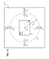
- FIG. 14 shows a fourth example of a sensor of an image capture system in a second embodiment of the invention.
- FIGS. 15A-15C show a fifth example of a sensor of an image capture system in a second embodiment of the invention
- FIG. 4 is a diagram representing an example of an image capture system in one possible embodiment of the invention.
- the image capture system 1 receives light originating from any scene S to be captured.
- the system 1 comprises an optical device L as well as a sensor C.
- the optical device L serves to focus the light emitted from the scene S on the sensor C.
- the optical device L and the sensor C form what is commonly referred to as an optical sensor module.
- the sensor C comprises a plurality of photosensitive elements (for example pixels). Each photosensitive element, in response to the amount of light that it receives, can deliver an electrical intensity which can be expressed as a certain numerical value. Thus the sensor C converts the light received from the optical device L into a series of numerical values corresponding to an image in digital form. This raw digital image may be affected by certain optical defects, including those presented above.
- the system 1 of the invention additionally comprises a determination means DET for determining at least one deviation.
- This determination means DET which may for example be a calculation module, within a processor for example, will receive the respective responses from certain photosensitive elements of the sensor C to an exposure of the image capture system to the scene S, as explained below, and will deduce at least one quantity G based on these responses.
- this quantity G can be representative of a state of the positioning of the optical device L relative to the sensor C.
- the determination means DET also has access to at least one reference quantity Gref.
- This quantity Gref corresponds for example to a situation in which the optical device L and the sensor C are correctly positioned. It will be used as a calibration measurement to which the quantity G will later be compared.
- Such a reference quantity Gref can also be defined by means such as initial characterization of the sensor C under different conditions, under several lighting angles for example. Such characterization will only be done once for a sensor type, and not, for example, systematically for each assembly of an optical device with a sensor. A quantity G subsequently obtained during everyday use of the system 1 can then be calculated based on any particular scene, and not require the use of a special scene.
- a deviation ⁇ between the quantity G and the reference quantity Gref is then calculated by the determination means DET.
- This deviation ⁇ yields, for example, an indication of the state of the positioning of the optical device L relative to the sensor C.
- This deviation ⁇ can be for example proportional to the difference G-Gref between these two quantities, or to their ratio G/Gref.
- This deviation ⁇ can also assume any other form allowing the mathematical comparison of the two quantities G and Gref.
- This deviation can also assume the form of an index in a table providing a correspondence between the reference data and predetermined data.
- the system 1 As introduced above, it is possible to detect an optical defect in the optical sensor module. From this detection, the system 1 can advantageously be recalibrated at a repair shop or in the factory, for example.
- the detection of an optical defect of the optical sensor module can be used for purposes other than for correcting said defect.
- it can be used as a diagnostic for the module, with no subsequent correction being made.
- a selection of one or more optical sensor modules can also be made by taking into account their respective optical defects if there are such.
- Other control mechanisms are also possible, as will be apparent to a person skilled in the art.
- the system 1 additionally comprises an estimation means DEF for estimating an optical defect and possibly a compensation means COMP for compensating for the optical defect.
- the means DEF receives the deviation ⁇ determined by the determination means DET, and estimates based on this deviation ⁇ the type and amplitude of the optical defect involved. The means DEF then sends this information to the compensation means COMP.
- This compensation means COMP also receives from the sensor C the raw digital image affected by the optical defects. Taking into account the information originating from the estimation means DEF, the compensation means COMP will be able to compensate for the determined optical defect, either wholly or in part.
- the compensation can occur without human intervention, for example at periodic intervals of time, or after the occurrence of certain events such as the system 1 suffering an impact.
- Such self-calibration is therefore more flexible than the prior art calibration mentioned in the introduction.
- the compensation in question can occur in various forms, particularly as a function of the defect detected.
- It may comprise mechanical actions, for example changing the tilt of the sensor and/or of the optical device in order to reduce or eliminate a defect in the relative tilt between these elements, a translation of the sensor and/or of the optical device within a plane substantially parallel to the sensor in order to reduce or eliminate a relative decentering defect between these elements, a translation of the sensor and/or the optical device in a direction substantially orthogonal to the sensor in order to reduce or eliminate a defocus defect of the lens relative to the sensor, or other actions.
- These mechanical actions are achieved for example by mechanical means, possibly controlled electronically.
- such compensation may comprise an appropriate digital processing.
- the digital processing may be implemented by the image capture system 1 itself, by digital processing means situated downstream from this system, or shared between the image capture system 1 and the digital processing means downstream.
- a decentering defect of the lens relative to the sensor can modify the properties of the vignetting phenomenon (illustrated in FIG. 2C and discussed above).
- the “original” vignetting phenomenon i.e. independent of the decentering, is generally corrected digitally either in the capture system, or by a specific means downstream.
- the digital correction may be based on a vignetting correction model, as a function, for example, of the image coordinates of the pixel to be processed, of the lens-sensor pair used, etc.
- X0, y0 are the coordinates of the center of the sensor and a[i] of the parameters related to the lens.
- x0 is advantageously replaced by x0+dx and y0 by y0+dx to digitally compensate for the decentering defect.
- a defocus defect (as illustrated in FIGS. 3A and 3B ) generates reduced sharpness in the image, because the focus distance is not optimum.
- Knowledge of the lens properties allows quantifying the reduction in sharpness as a function of the defocus.
- the amount of the sharpness reduction can be known, and it can be compensated for digitally by a sharpening technique (such as deconvolution or other techniques).
- the compensation by the compensation means COMP of the system 1 can be partial and be limited to modifying the received image in order to return an image having a certain degree of defect which can then be corrected by said digital processing means situated downstream. It may also consist of changing the parameters of the model used in the processing means located downstream, without affecting the image.
- FIG. 5 is a flowchart illustrating a control method for an image capture system in one embodiment of the invention, as described for example in FIG. 4 .
- the determination means DET obtains respective responses from certain photosensitive elements of the sensor C of the image capture system 1 . These different photosensitive elements are at least two in number.
- the determination means DET determines, during a second step 200 , the deviation ⁇ between a quantity G, deduced from the response obtained during the step 100 , and a reference quantity Gref, determined as explained above. This deviation allows detecting a possible optical defect in the capture system, such as improper positioning in the optical sensor module for example.
- the method additionally comprises a step 300 , during which the estimation means DEF estimates the optical defect of the capture system 1 based on the deviation ⁇ determined during the second step 200 .
- the compensation means COMP it then becomes possible, during a fourth step 400 , for the compensation means COMP to implement a complete or partial compensation for the optical defect estimated during step 300 .
- FIGS. 6A and 6B illustrate the optical sensor module of an image capture system according to a first embodiment of the invention, intended to detect for example an optical defect related to a relative tilt between the sensor and the optical device as presented above in FIGS. 1A-1C .
- the optical device L and the sensor C of the image capture system are represented without the housing or the optical support which may possibly be part of the system, as these last elements are not essential to understanding this embodiment. Also represented is the deviation determination means DET receiving the response from certain elements of the sensor C.
- the sensor C of the invention comprises a region Z in which is situated a plurality of photosensitive elements Z 1 , Z 2 , . . . , Z n .
- Each of these photosensitive elements is sensitive to a particular spectral band. Of these photosensitive elements, some may be sensitive to at least a portion of the spectral bands in common. It is also possible to have identical photosensitive elements among the photosensitive elements of the sensor C, which are therefore sensitive to the same spectral band.
- the sensor C has, among the plurality of photosensitive elements Z 1 , Z 2 , . . . , Z n , at least two photosensitive elements E 1 and E 1 , situated at different locations in the sensor and sensitive to at least one common spectral band. Due to their different positions, the light reaching these elements will come from a different angle, and therefore their respective responses in terms of intensities I(E 1 ) and I(E 1 ′) representative of the amount of light received by each of these two elements will be different. This difference in intensity response can be expressed as a parameter G, corresponding to the quantity presented above, which is a function of the intensity responses I(E 1 ) and I(E 1 ′).
- the parameter G calculated using one of the above formulas will have a reference value Gref, corresponding to the optimum position in terms of parallelism of the optical sensor module.
- the reference parameter Gref can also be calculated based on measurements of responses under initial illumination of the sensor alone, under certain specific conditions, such as particular angles of lighting for example. Such a reference value Gref can then be stored in the determination means DET, for example.
- the parameter G has a value different from Gref, which indirectly reflects this tilt defect.
- the relative comparison of this value G with the reference value Gref will provide a deviation ⁇ representing any tilt defect, which enables the detection of this defect. It will then be possible to have the optical system repaired or possibly to determine the optical defect and estimate it in order to initiate a compensatory action in the capture system itself.
- the elements E 1 and E 1 ′ for which the responses are used by the determination means DET, may be chosen from among any of the photosensitive elements Z i of the sensor C, as long as they are sensitive to at least one common spectral band.
- their intensity responses will have a high probability of being substantially homogeneous in terms of image content, and can be compared directly with no need to apply equalization processing between different spectral bands having spectral responses of varying sensitivity.
- Other functions may be used to the extent that they are indicative of a difference in the light intensity received by these two elements. This allows eliminating, by mathematical comparison, the intensity component common to the two elements E 1 and E 1 ′, corresponding to the content of the captured image in the common spectral band. The intensity component related to the tilt angle ⁇ can then more easily be distinguished.
- the two elements E 1 and E 1 ′ for which the response is used by the means DET are chosen to be near neighbors. They are first-nearest neighbors, meaning adjacent to each other, or second-nearest neighbors, meaning they are not adjacent to each other but there is at least one other photosensitive element to which they are both adjacent, for example, although this is not a limiting example.
- This concept of near neighbors is illustrated in FIG. 7 .
- FIG. 7 shows a conventional sensor C′, viewed from above, comprising a plurality of photosensitive elements.
- the photosensitive elements of a sensor are usually arranged in a bi-directional grid.
- the first-nearest neighbors are those adjacent to V 0 in one of the two directions of the grid.
- These first-nearest neighboring elements are the elements V 1 in FIG. 7 .
- the second-nearest neighboring elements V 2 of V 0 are the first-nearest neighboring elements of the first-nearest neighboring elements V 1 of the element V 0 , this element V 0 itself being excluded.
- the third-nearest neighboring elements V 3 of V 0 are the first-nearest neighboring elements of the second-nearest neighboring elements V 2 of the element V 0 , excluding the elements V 1 , and so on.
- This advantageous characteristic allows obtaining a more reliable measurement, to the extent that the captured image may have areas that are more or less dark at different locations.
- comparing the intensity received from a first element situated in a dark region to the intensity received from a second element situated in a brighter region would distort the measurement of the tilt angle ⁇ . If the two elements are chosen within the same region of limited size, they will receive relatively uniform brightness information, and therefore the comparison of their respective intensities will more effectively eliminate the unnecessary intensity component, which will better emphasize the component related to the angle ⁇ .
- the invention is not limited to using the response from first- or second-nearest neighbor elements.
- the above reasoning with only two photosensitive elements E 1 and E 1 ′ can be made with a plurality of pairs of photosensitive elements (E 1 ,E 1 ′), advantageously sensitive to a same common spectral band.
- Increasing the number of elements used to give a response eliminates any image transition zones in which the method would no longer work with only two elements, if these elements were on each side of this transition zone. This additionally allows reducing the effect of noise on the measurement.
- a series of specific reference parameters Gref i are obtained, determined for each pair of photosensitive elements (E i , E i ′) as a function of their position in the image field.
- Such specific parameters may be determined initially, for example by illuminating the sensor from different angles, and stored in a memory associated with the capture system 1 in order to perform the comparison at a later time. This series of specific parameters can be stored in the determination means DET.
- a general deviation ⁇ G may possibly be calculated from these specific deviations ⁇ i .
- This general deviation ⁇ G can be, for example, the mean of all specific deviations ⁇ i , or their median value, or any other value allowing a general characterization of all these specific deviations ⁇ .
- Any later estimation of an optical defect of the image capture system can be based on a general deviation ⁇ G . In a variant, it can be based on some or all of the specific deviations ⁇ i .
- Calculating a general deviation ⁇ G in the manner indicated above is particularly advantageous when the different pairs of photosensitive elements (E i ,E i ′) from which the response is used are substantially near each other.
- the reference quantity changes as a function of the image field, one can envisage, in the case where the different pairs of photosensitive elements (E i ,E i ′) from which the response is used are not near one another, calculating specific angles ⁇ i for each of the pairs in order to obtain from them a general angle ⁇ G corresponding for example to the mean of the specific angles ⁇ i .
- This example of two pairs of elements is of course not limiting.
- the determination means DET uses the responses from a plurality of pairs (E 1 , E i ′), these pairs are part of a selected region E of the sensor C.
- This region E which represents a subpart of the surface of the sensor, can be chosen for receiving a homogeneous region of the image excluding the regions with high frequencies, synonymous with transitions and therefore with potential measurement errors.
- Such a region can be determined by methods known to a person skilled in the art, for example by using sensor noise curves, or using information on other channels, situated in other spectral bands besides those of the photosensitive elements used.
- FIG. 8 partially illustrates an image capture system having an exemplary sensor comprising a common example of a color filter, called a Bayer filter, often found in current digital image capture devices.
- the sensor C is formed by superimposing a color filter FIL and a light-sensitive substrate SUB.
- the light coming from a source S and passing through an optical device L as described above, illuminates the color filter F.
- This filter spatially filters the light into different spectral bands and breaks it apart into beams of different colors, which will strike the substrate SUB at different locations.
- Such an arrangement allows dividing the light into different components in a defined pattern, for example a grid, for more appropriate processing and transmission.
- a color filter FIL which divides the filtered light into its three components: red, blue, and green. This allows receiving intensities at different points on the substrate which correspond to these different components, and using them to reconstruct the image at a later time.
- the Bayer filter consists of the repetition in two dimensions of a base pattern Mb of 2 ⁇ 2 filtering elements, an element B to filter blue, an element R to filter red, and two elements Gr and Gb to filter green.
- the green spectral band is the central band in the light spectrum and generally contains more information than the others. As the human eye is more sensitive to this band, the choice was made to have two elements Gr and Gb for detecting green in this type of filter.
- a typical defect affecting this type of filter is what is referred to as crosstalk.
- crosstalk means the fact that when photons reach a photosensitive element, they are partially deflected towards neighboring photosensitive elements.
- the invention makes use of such a phenomenon, normally detrimental, in a positive way in order to better detect an optical defect.
- the comparison of the intensities I(E 1 ) and I(E 1 ′) of the responses as explained above, will be applied to the response intensities of two elements Gr and Gb of a same base pattern Mb of a Bayer filter. As these two elements are close to each other, they undergo a crosstalk phenomenon and their response therefore contains a component of correlated information, which can be even more easily eliminated by comparing their two intensities, which will improve the observation of the tilt angle ⁇ .
- the quantity G as defined above will therefore issue from the comparison of the intensity I(Gr) received by an element Gr and the intensity I(Gb) received by an element Gb of a same base pattern.
- difference means the measurement used for the comparison between these two values I(Gr) and I(Gb), expressed as a percent.
- FIG. 9 illustrates this image field concept.
- the sensor presented in the example in FIG. 9 has the rectangular “4:3” form, meaning its image width h is equal to 4/3 the image height v.
- image field is used to indicate the distance relative to the center of the sensor in FIG. 9 .
- a position at 100% in the image field corresponds to a position on one of the corners of the rectangular sensor, which corresponds to a maximum distance relative to this center equal to the diagonal of the rectangle.
- a position on one of its sides is at 80% or 60% in the image field (absolute value), with the sign indicating which side relative to the center.
- the center of the sensor is at 0% in the image field.
- FIG. 10A shows a curve representing the chief ray angle (CRA) property of a lens, as a function of the position in the image field.
- CRA chief ray angle
- FIG. 10B shows a curve characterizing the difference between the photosensitive elements Gr and Gb, expressed as percents, for a given sensor, as a function of the angle of incidence of the rays on the elements for a given position in the image field.
- the given position corresponds to 60% in the field on the X axis of the sensor. This curve does not depend on the optical device associated with the sensor.
- FIG. 10C shows a record of the difference, in percents, between the intensities received by the photosensitive elements Gr and Gb belonging to the same base pattern, as a function of the position on a horizontal axis X of a rectangular sensor.
- the abscissa are expressed as image field percentages as explained above.
- such an estimate of the difference between the intensities received by the photosensitive elements Gr and Gb of a module can be done based on an image, a region of the image, or a set of regions of the image.
- such an estimate of the difference between intensities of the elements Gr and Gb is also possible on a video stream, on a subsampled version of the image.
- the estimate can be done with prior knowledge of the model of crosstalk variation between elements Gr and Gb, as illustrated in FIG. 10C .
- the measurements made on the image then serve to adapt to a parametric model, which allows decreasing measurement-related errors and having more advanced applications based on these estimates.
- photosensitive elements sensitive to the color green were used for measuring the tilt defect, because the Bayer filter has the particular characteristic of having a microstructure with two distinct green elements.
- the use of this particular spectral band is advantageous, because the spectral response in this band is more sensitive, particularly in the human eye. Also, as this spectral band is located in the middle of the visible spectrum, most images will have components in this band, and in any case many more than with the other spectral bands red and blue. Thus any image can be used to detect a relative tilt angle, without needing to make a specific choice of a certain type of image for performing the measurement.
- the invention is not limited to this example, and any elements sensitive to another color can be used.
- FIG. 11A shows a top view of a sensor C that is part of an optical sensor module similar to those presented above.
- a sensor advantageously has a central image capture region Z, comprising a certain number of photosensitive elements Z i dedicated to capturing incident photons in order to reconstruct an image, surrounded by a peripheral region P which does not comprise pixels dedicated specifically to capturing images and therefore not contributing to the image capture.
- the central region Z is described in this example as being rectangular, with a center O Z situated at the intersection of its diagonals, meaning at the intersection of its two orthogonal axes of symmetry X and Y.
- any other form of image capture region can be envisaged, such as a circular form.
- the optical device L associated with the sensor C in the image capture system of the invention and not represented in this top view, will illuminate the sensor C with light coming from the source S, in an illuminated region of a shape which depends on the shape of the device L itself.
- the optical device L is circular and will therefore present a circle of illumination I ref on the sensor C.
- the light intensity received outside this circle of illumination I ref is practically zero.
- the size of this circle will depend on the distance separating the optical device L and the sensor C, as illustrated in FIGS. 3A and 3B above.
- FIG. 11A represents the case where the optical device L is centered on the sensor C, meaning the case where the center of the circle of illumination I ref and the center O Z of the central region Z coincide, and an optimal focus distance F separates the optical device L and the sensor C.
- the circle of illumination I ref then has a radius R Iref and constitutes a reference circle of illumination, corresponding to an optimum position of the optical device L in terms of decentering and defocus relative to the sensor C.
- the sensor C has a certain number of photosensitive elements P i situated in the peripheral region P of the sensor C and having a response which allows detecting a decentering or defocus defect as respectively illustrated in FIGS. 2A-2D and 3 A- 3 B above.
- These photosensitive elements P i can, for example, have a binary digital response, meaning a response of “0” when the light intensity received is less than a first threshold and a response of “1” when the light intensity received is greater than a second threshold which is greater than the first threshold.
- the invention is not, however, limited to this type of photosensitive element, and any type of element that allows distinguishing a level of high light intensity from a level of low light intensity can be used.
- the sensor C has a first photosensitive element P 1 situated inside the reference circle of illumination I ref , as well as a second photosensitive element P 2 situated outside the reference circle of illumination I ref .
- Gref the value of Gref will be non-zero.
- FIG. 11 b illustrates two cases where the optical device L is decentered relative to the sensor C in the direction of its X axis.
- the optical device L In a first case where the optical device L is offset to the right of the sensor C, it will project a circle of illumination I 1 of center O I1 on the sensor C.
- the two elements P 1 and P 2 are part of the circle of illumination I 1 , and the quantity G, determined based on their intensity response in a manner identical to the reference quantity Gref, will have a value equal to 2.
- the fact that this deviation ⁇ is substantial will be indicative of a decentering defect. For example, if the deviation ⁇ corresponds to the difference between G and Gref, ⁇ is no longer zero but here has the value of “1”, indicative of an optical positioning defect.
- FIG. 11C illustrates two other cases, where the optical device L is defocused relative to the sensor C.
- the circle of illumination I 3 projected onto the sensor C will be larger than the reference circle of illumination I ref .
- the two elements P 1 and P 2 are part of the circle of illumination I 3 , similarly to the case presented above with FIG. 11B where the optical device was decentered to the right of the sensor C, and the quantity G, determined similarly to the previous cases, will have a value of “2”.
- a decentering or defocus optical defect can therefore be detected, without necessarily needing to distinguish what type.
- the following examples concern a sensor which advantageously allows distinguishing the type of optical defect involved.
- a second example of a sensor C is represented in a top view in FIG. 12 .
- This sensor C is similar to the one presented in FIGS. 11A-11C , except that it has two photosensitive elements P 3 and P 4 , situated in the peripheral region P, for example inside the circle of illumination I ref , and on a Y axis passing through the center O Z of the rectangular central region Z, advantageously at equal distances from the center O Z of the region, in order to obtain more concrete information.
- This Y axis can for example be an axis of symmetry of the region Z.
- the reference quantity Gref may correspond to the sum of the responses of the two elements P 3 and P 4 , for example, which here gives a value of “2”.
- the optical device L is decentered along the Y axis, in the downward direction for example, the element P 3 will no longer be illuminated while the element P 4 will remain so.
- the quantity G will then only have a value of “1”. If, in a second case, the optical device L is closer to the sensor C, the circle of illumination will shrink to the point where the two elements P 3 and P 4 are no longer illuminated. The quantity G then assumes the value of zero.
- elements P 3 and P 4 are situated outside the circle of illumination I ref , one can detect an increase in the distance between the optical device L and the sensor C in the same manner.
- Determination of the deviation ⁇ between the quantity G and the reference quantity Gref then allows distinguishing the type of optical defect involved. If one considers, for example, that the deviation ⁇ corresponds to the difference between G and Gref, then the absolute value of this deviation ⁇ will be “1” when there is decentering, and “2” when the optical device L and the sensor C are too close together. The deviation ⁇ is therefore a good indicator of the type of defect.
- a decentering along the axis Y of the region Z can be detected and differentiated from a defect related to the optical device L being too close to the sensor C.
- a third example, illustrated in FIG. 13 consists of extrapolating from the example in FIG. 12 by additionally using the response of two other photosensitive elements P 5 and P 6 , still located within the peripheral region P, inside the circle of illumination I ref and on the X axis of symmetry of the central rectangular region Z, at equal distances from the center O Z of the region.
- the reference quantity Gref can then correspond to a pair of relative reference quantities (Gref 1 , Gref 2 ) respectively corresponding to the sum of the responses from elements P 3 and P 4 , and from elements P 5 and P 6 , for example.
- the reference quantity Gref here will have the value (2,2).
- the deviation ⁇ calculated as (G 1 ⁇ Gref 1 , G 2 ⁇ Gref 2 ) then has the value (1,0) which indicates a decentering along the Y axis. If the quantity G has the value (2,1), the deviation ⁇ then has the value (0,1), which indicates a decentering along the X axis. Lastly, if the quantity G has the value (0,0), the deviation ⁇ then has the value (2,2), which indicates a focus defect due to the optical device L and the sensor being too close together.
- a decentering along the Y or X axis of the region Z can be detected and differentiated from a defect related to the optical device L being too close to the sensor C.
- a fourth example, illustrated in FIG. 14 consists of extrapolating the example in FIG. 13 by additionally using the response from four other photosensitive elements P 3 ′,P 4 ′,P 5 ′ and P 6 ′ situated within the peripheral region P, outside the circle of illumination I ref , on the X and Y axes of the rectangular central region Z, at equal distances from the center O Z of the region.
- the reference quantity Gref can then correspond to a series of four relative reference quantities Gref i for each of the pairs of elements (P i ,P i ′) corresponding for example to the sum of the associated responses from elements P i and P i ′.
- the general reference quantity Gref here will have the value (1,1,1,1).
- the deviation ⁇ then has the value ( ⁇ 1, ⁇ 1, ⁇ 1, ⁇ 1), indicating a focus defect due to the optical device L being too close to the sensor C.
- the general quantity G has the value (2,2,2,2), meaning all the elements are illuminated, the deviation ⁇ then has the value (1,1,1,1), indicating a focus defect due to the optical device L being too far away from the sensor C.
- FIG. 15A shows a top view of a sensor C similar to the one presented in the above FIGS. 12-14 .
- a sensor has secondary regions Pa, Pb, Pc and Pd, which are part of the peripheral region P in which are found a certain number of respective photosensitive elements Pa i , Pb i , Pc i and Pd i , situated on the X or Y axis of symmetry of the central region.
- each secondary region comprises four photosensitive elements, but the invention is not limited to this number.
- solely the secondary regions Pa and Pb could be used.
- the four photosensitive elements Pa i are spaced apart from one another by a given distance ⁇ .
- ⁇ the distance between the photosensitive elements.
- the sensor in FIG. 15A is illuminated by a circle of illumination I ref identical to the one in FIG. 11A , meaning it corresponds to the optimum positioning of the optical device L relative to the sensor C in terms of focus and decentering.
- the circle of illumination I ref passes through all secondary regions.
- the circle of illumination I ref passes between elements Pa 2 and Pa 3 , which implies that the elements Pa 1 and Pa 2 are substantially well illuminated while the elements Pa 3 and Pa 4 are barely or not at all illuminated.
- Such a quantity can for example be the sum of the intensities received by the photosensitive elements of the region Pa.
- this sum is equal to the value “2” and reflects the fact that the circle of illumination passes between the elements Pa 2 and Pa 3 .
- a similar calculation can be made for each of the other secondary regions.
- FIG. 15B illustrates the case where the optical device L is off-center relative to the sensor C along the direction of its X axis.
- the circle of illumination I 5 having center O I5 passes between photosensitive elements Pc 3 and Pc 4 of the secondary region Pc, as well as between the photosensitive elements Pd 2 and Pd 1 of the secondary region Pd.
- the relative quantity G d of the region Pd will therefore decrease relative to the optimum case and will have the value “1” in the present example, while the relative quantity G c of the region Pc will increase relative to the optimum case and have the value “3”.
- the deviations between the relative quantities of the regions Pa-Pd (here having the respective values “2”, “2”, “3”, “1”) and the relative reference quantities for these same regions (which all have values of “2” in the present case), provide information on the decentering of the optical device L towards the right of the sensor C as well as its amplitude, with an uncertainty corresponding to the distance ⁇ between the photosensitive elements of the same region.
- FIG. 15C illustrates two other cases, this time where the optical device L is defocused relative to the sensor C, with no decentering between the device L and the sensor C.
- the circle of illumination I 6 passes between the first and second photosensitive elements of each secondary region.
- the quantities G relative to each region will therefore decrease relative to the optimum case and have the value “1” in this example.
- the comparison of these relative quantities G to the reference relative quantities Gref i which have the value “2” in this example, will indicate a decrease in the radius of the circle of illumination, and therefore a decrease in the distance separating the sensor C from the optical device L.
- the fact that the relative quantities for opposing secondary regions decrease simultaneously by the same magnitude means there is no decentering defect.
- the circle of illumination I 7 passes between the second and third photosensitive elements of each secondary region.
- the relative quantities G i of each region will therefore increase relative to the optimum case and have the value “3” in this example.
- the comparison of these relative quantities G i relative to the reference relative quantities Gref i which still have the value “2” in this example, will indicate an increase in radius of the circle of illumination, and therefore an increase in the distance separating the sensor C from the optical device L.
- the fact that the relative quantities of opposing secondary regions increase simultaneously in the same proportions means that there is no decentering defect.
- each optical defect was presented separately for purposes of simplification. It is obvious, however, that a decentering defect may occur simultaneously with a focusing defect. By its configuration, the optical sensor module presented in FIGS. 15A-15C will be able to detect and estimate each of the defects independently.
- the defect can be one of the optical defects mentioned above, or any other conceivable optical defect detectable from the respective responses of at least some of the photosensitive elements of the sensor.
Landscapes
- Engineering & Computer Science (AREA)
- Multimedia (AREA)
- Signal Processing (AREA)
- Health & Medical Sciences (AREA)
- Biomedical Technology (AREA)
- General Health & Medical Sciences (AREA)
- Studio Devices (AREA)
Abstract
Description
-
- a sensor comprising a plurality of photosensitive elements,
- an optical device for focusing the light emitted from a scene on the sensor,
- a means for determining at least one deviation between at least one quantity deduced from respective responses from at least some of the photosensitive elements of the sensor to an exposure of the image capture system to any scene, and at least one reference quantity.
Claims (15)
Applications Claiming Priority (3)
| Application Number | Priority Date | Filing Date | Title |
|---|---|---|---|
| FR0950192 | 2009-01-14 | ||
| FR0950192A FR2941067B1 (en) | 2009-01-14 | 2009-01-14 | OPTICAL DEFECT CONTROL IN AN IMAGE CAPTURE SYSTEM |
| PCT/FR2010/050034 WO2010081982A1 (en) | 2009-01-14 | 2010-01-11 | Monitoring of optical defects in an image capture system |
Publications (2)
| Publication Number | Publication Date |
|---|---|
| US20110273569A1 US20110273569A1 (en) | 2011-11-10 |
| US8634004B2 true US8634004B2 (en) | 2014-01-21 |
Family
ID=40532679
Family Applications (1)
| Application Number | Title | Priority Date | Filing Date |
|---|---|---|---|
| US13/144,293 Expired - Fee Related US8634004B2 (en) | 2009-01-14 | 2010-01-11 | Monitoring of optical defects in an image capture system |
Country Status (4)
| Country | Link |
|---|---|
| US (1) | US8634004B2 (en) |
| EP (1) | EP2377306A1 (en) |
| FR (1) | FR2941067B1 (en) |
| WO (1) | WO2010081982A1 (en) |
Families Citing this family (13)
| Publication number | Priority date | Publication date | Assignee | Title |
|---|---|---|---|---|
| JPWO2010055809A1 (en) * | 2008-11-12 | 2012-04-12 | コニカミノルタオプト株式会社 | Image pickup apparatus adjustment method and image pickup apparatus |
| US8350934B2 (en) | 2010-10-21 | 2013-01-08 | Taiwan Semiconductor Manufacturing Co., Ltd. | Color image sensor array with color crosstalk test patterns |
| US8924168B2 (en) | 2011-01-27 | 2014-12-30 | General Electric Company | Method and system to detect actuation of a switch using vibrations or vibration signatures |
| TW201326738A (en) * | 2011-12-16 | 2013-07-01 | Hon Hai Prec Ind Co Ltd | Test device and method for camera module |
| JP2019009653A (en) * | 2017-06-26 | 2019-01-17 | アイホン株式会社 | Camera module adjustment method in intercom device |
| CN112689752B (en) | 2018-09-20 | 2025-04-29 | 美国西门子医学诊断股份有限公司 | Systems, methods and apparatus for autonomous diagnostic verification of optical components of vision-based inspection systems |
| US11277544B2 (en) | 2019-08-07 | 2022-03-15 | Microsoft Technology Licensing, Llc | Camera-specific distortion correction |
| JP7692476B2 (en) | 2020-10-02 | 2025-06-13 | グーグル エルエルシー | Image capture doorbell device |
| CN116829927A (en) | 2021-02-04 | 2023-09-29 | 美国西门子医学诊断股份有限公司 | Device and method for detecting defects in machine vision systems |
| US11663704B2 (en) | 2021-04-28 | 2023-05-30 | Microsoft Technology Licensing, Llc | Distortion correction via modified analytical projection |
| EP4381729A1 (en) * | 2021-08-02 | 2024-06-12 | Google LLC | Asymmetric camera sensor positioning for enhanced package detection |
| US12493197B2 (en) | 2022-01-04 | 2025-12-09 | Meta Platforms Technologies, Llc | Camera device assembled with lens-to-sensor distance that reduces auto-focusing actuation power in macro mode |
| DE102024202574A1 (en) | 2024-03-19 | 2025-09-25 | Robert Bosch Gesellschaft mit beschränkter Haftung | Computer-implemented method for optimizing the assembly of lenses on imaging devices |
Citations (27)
| Publication number | Priority date | Publication date | Assignee | Title |
|---|---|---|---|---|
| WO2000079784A1 (en) | 1999-06-04 | 2000-12-28 | The Trustees Of Columbia University In The City Of New York | Apparatus and method for high dynamic range imaging using spatially varying exposures |
| JP2001186409A (en) * | 1999-12-24 | 2001-07-06 | Toyota Autom Loom Works Ltd | Image distortion correction device |
| WO2003043308A2 (en) | 2001-11-13 | 2003-05-22 | Koninklijke Philips Electronics N.V. | Method for calibration and correction of radial lens distortion |
| US7032472B2 (en) * | 2002-05-10 | 2006-04-25 | Caterpillar Inc. | Counterbalance for linkage assembly |
| US20060125945A1 (en) * | 2001-08-07 | 2006-06-15 | Satoshi Suzuki | Solid-state imaging device and electronic camera and shading compensaton method |
| US7071966B2 (en) * | 2003-06-13 | 2006-07-04 | Benq Corporation | Method of aligning lens and sensor of camera |
| WO2007055179A1 (en) | 2005-11-09 | 2007-05-18 | Sharp Kabushiki Kaisha | Device for correcting quantity of ambient light, method for correcting quantity of ambient light, electronic information apparatus, control program and readable recording medium |
| US20070133893A1 (en) * | 2005-12-14 | 2007-06-14 | Micron Technology, Inc. | Method and apparatus for image noise reduction |
| US20070165119A1 (en) | 2005-11-01 | 2007-07-19 | Olympus Corporation | Image processing apparatus for correcting defect pixel in consideration of distortion aberration |
| US7352403B2 (en) * | 2003-07-07 | 2008-04-01 | Benq Corporation | Method for adjusting relative position of lens module by using uniform light source |
| US20080111912A1 (en) * | 2006-11-09 | 2008-05-15 | Mei-Ju Chen | Methods and apparatuses for generating information regarding spatial relationship between a lens and an image sensor of a digital imaging apparatus and related assembling methods |
| US20080218607A1 (en) | 2007-03-08 | 2008-09-11 | Pentax Corporation | Distortion correction for photographing device |
| US20110001848A1 (en) * | 2009-07-02 | 2011-01-06 | Hugh Phu Nguyen | Two-dimensional lens shading correction |
| US7907185B2 (en) * | 2007-07-16 | 2011-03-15 | Aptina Imaging Corporation | Lens correction logic for image sensors |
| US20110074961A1 (en) * | 2009-09-29 | 2011-03-31 | Chi Mei Communication Systems, Inc. | System and method for testing a digital camera module |
| US7961973B2 (en) * | 2004-09-02 | 2011-06-14 | Qualcomm Incorporated | Lens roll-off correction method and apparatus |
| US20110141292A1 (en) * | 2009-12-14 | 2011-06-16 | Hong Fu Jin Precision Industry (Shenzhen) Co., Ltd. | Method and system for measuring deflection angle of a camera lens |
| US8049795B2 (en) * | 2005-12-28 | 2011-11-01 | Mtekvision Co., Ltd. | Lens shading compensation apparatus and method, and image processor using the same |
| US8054350B2 (en) * | 2007-02-23 | 2011-11-08 | Samsung Electronics Co., Ltd. | Shade correction for lens in image sensor |
| US20110310254A1 (en) * | 2010-06-21 | 2011-12-22 | Barnes Iv George C | Optical Alignment Structures And Associated Methods |
| US8085391B2 (en) * | 2007-08-02 | 2011-12-27 | Aptina Imaging Corporation | Integrated optical characteristic measurements in a CMOS image sensor |
| US20120081583A1 (en) * | 2010-09-21 | 2012-04-05 | Sony Corporation | Aberration correction apparatus, aberration correction method, and program |
| US8164633B2 (en) * | 2008-02-28 | 2012-04-24 | Kddi Corporation | Calibration apparatus and method for imaging devices and computer program |
| US20120293670A1 (en) * | 2011-05-17 | 2012-11-22 | Digital Imaging Systems Gmbh | Fast measurement of alignment data of a camera system |
| US8339463B2 (en) * | 2010-12-31 | 2012-12-25 | Altek Corporation | Camera lens calibration system |
| US20130050537A1 (en) * | 2011-08-26 | 2013-02-28 | Novatek Microelectronics Corp. | Image correction device and image correction method |
| US8405711B2 (en) * | 2007-01-09 | 2013-03-26 | Capso Vision, Inc. | Methods to compensate manufacturing variations and design imperfections in a capsule camera |
Family Cites Families (1)
| Publication number | Priority date | Publication date | Assignee | Title |
|---|---|---|---|---|
| EP2018047A1 (en) * | 2007-06-15 | 2009-01-21 | IEE INTERNATIONAL ELECTRONICS & ENGINEERING S.A. | Method for contamination detection in a TOF range camera |
-
2009
- 2009-01-14 FR FR0950192A patent/FR2941067B1/en not_active Expired - Fee Related
-
2010
- 2010-01-11 US US13/144,293 patent/US8634004B2/en not_active Expired - Fee Related
- 2010-01-11 EP EP10706293A patent/EP2377306A1/en not_active Withdrawn
- 2010-01-11 WO PCT/FR2010/050034 patent/WO2010081982A1/en not_active Ceased
Patent Citations (29)
| Publication number | Priority date | Publication date | Assignee | Title |
|---|---|---|---|---|
| WO2000079784A1 (en) | 1999-06-04 | 2000-12-28 | The Trustees Of Columbia University In The City Of New York | Apparatus and method for high dynamic range imaging using spatially varying exposures |
| JP2001186409A (en) * | 1999-12-24 | 2001-07-06 | Toyota Autom Loom Works Ltd | Image distortion correction device |
| US20060125945A1 (en) * | 2001-08-07 | 2006-06-15 | Satoshi Suzuki | Solid-state imaging device and electronic camera and shading compensaton method |
| WO2003043308A2 (en) | 2001-11-13 | 2003-05-22 | Koninklijke Philips Electronics N.V. | Method for calibration and correction of radial lens distortion |
| US7032472B2 (en) * | 2002-05-10 | 2006-04-25 | Caterpillar Inc. | Counterbalance for linkage assembly |
| US7071966B2 (en) * | 2003-06-13 | 2006-07-04 | Benq Corporation | Method of aligning lens and sensor of camera |
| US7352403B2 (en) * | 2003-07-07 | 2008-04-01 | Benq Corporation | Method for adjusting relative position of lens module by using uniform light source |
| US7961973B2 (en) * | 2004-09-02 | 2011-06-14 | Qualcomm Incorporated | Lens roll-off correction method and apparatus |
| US20070165119A1 (en) | 2005-11-01 | 2007-07-19 | Olympus Corporation | Image processing apparatus for correcting defect pixel in consideration of distortion aberration |
| US20090219419A1 (en) | 2005-11-09 | 2009-09-03 | Sharp Kabushiki Kaisha | Peripheral Light Amount Correction Apparatus, Peripheral Light Amount Correction Method, Electronic Information Device, Control Program and Readable Recording Medium |
| US8106976B2 (en) * | 2005-11-09 | 2012-01-31 | Sharp Kabushiki Kaisha | Peripheral light amount correction apparatus, peripheral light amount correction method, electronic information device, control program and readable recording medium |
| WO2007055179A1 (en) | 2005-11-09 | 2007-05-18 | Sharp Kabushiki Kaisha | Device for correcting quantity of ambient light, method for correcting quantity of ambient light, electronic information apparatus, control program and readable recording medium |
| US20070133893A1 (en) * | 2005-12-14 | 2007-06-14 | Micron Technology, Inc. | Method and apparatus for image noise reduction |
| US8049795B2 (en) * | 2005-12-28 | 2011-11-01 | Mtekvision Co., Ltd. | Lens shading compensation apparatus and method, and image processor using the same |
| US20080111912A1 (en) * | 2006-11-09 | 2008-05-15 | Mei-Ju Chen | Methods and apparatuses for generating information regarding spatial relationship between a lens and an image sensor of a digital imaging apparatus and related assembling methods |
| US8405711B2 (en) * | 2007-01-09 | 2013-03-26 | Capso Vision, Inc. | Methods to compensate manufacturing variations and design imperfections in a capsule camera |
| US8054350B2 (en) * | 2007-02-23 | 2011-11-08 | Samsung Electronics Co., Ltd. | Shade correction for lens in image sensor |
| US20080218607A1 (en) | 2007-03-08 | 2008-09-11 | Pentax Corporation | Distortion correction for photographing device |
| US7907185B2 (en) * | 2007-07-16 | 2011-03-15 | Aptina Imaging Corporation | Lens correction logic for image sensors |
| US8085391B2 (en) * | 2007-08-02 | 2011-12-27 | Aptina Imaging Corporation | Integrated optical characteristic measurements in a CMOS image sensor |
| US8164633B2 (en) * | 2008-02-28 | 2012-04-24 | Kddi Corporation | Calibration apparatus and method for imaging devices and computer program |
| US20110001848A1 (en) * | 2009-07-02 | 2011-01-06 | Hugh Phu Nguyen | Two-dimensional lens shading correction |
| US20110074961A1 (en) * | 2009-09-29 | 2011-03-31 | Chi Mei Communication Systems, Inc. | System and method for testing a digital camera module |
| US20110141292A1 (en) * | 2009-12-14 | 2011-06-16 | Hong Fu Jin Precision Industry (Shenzhen) Co., Ltd. | Method and system for measuring deflection angle of a camera lens |
| US20110310254A1 (en) * | 2010-06-21 | 2011-12-22 | Barnes Iv George C | Optical Alignment Structures And Associated Methods |
| US20120081583A1 (en) * | 2010-09-21 | 2012-04-05 | Sony Corporation | Aberration correction apparatus, aberration correction method, and program |
| US8339463B2 (en) * | 2010-12-31 | 2012-12-25 | Altek Corporation | Camera lens calibration system |
| US20120293670A1 (en) * | 2011-05-17 | 2012-11-22 | Digital Imaging Systems Gmbh | Fast measurement of alignment data of a camera system |
| US20130050537A1 (en) * | 2011-08-26 | 2013-02-28 | Novatek Microelectronics Corp. | Image correction device and image correction method |
Non-Patent Citations (1)
| Title |
|---|
| International Search Report in Application No. PCT/FR2010/050034. |
Also Published As
| Publication number | Publication date |
|---|---|
| FR2941067A1 (en) | 2010-07-16 |
| EP2377306A1 (en) | 2011-10-19 |
| FR2941067B1 (en) | 2011-10-28 |
| WO2010081982A1 (en) | 2010-07-22 |
| US20110273569A1 (en) | 2011-11-10 |
Similar Documents
| Publication | Publication Date | Title |
|---|---|---|
| US8634004B2 (en) | Monitoring of optical defects in an image capture system | |
| US9894302B2 (en) | Imaging apparatus, image processing method, and program | |
| US7812881B2 (en) | Imaging device, camera and image processing method | |
| US7711261B2 (en) | Imaging device, camera and image processing method | |
| US8269880B2 (en) | Imaging device, camera and image processing method | |
| US8736683B2 (en) | Method for estimating a defect in an image-capturing system, and associated systems | |
| US9479688B2 (en) | Image capture apparatus | |
| JP6004221B2 (en) | Image processing device | |
| JP2015534734A (en) | System and method for detecting defective camera arrays, optical arrays, and sensors | |
| US10771762B2 (en) | Image processing apparatus, image pickup apparatus, image processing method, and non-transitory computer-readable storage medium that correct a parallax image based on a correction value calculated using a captured image | |
| WO2018143340A1 (en) | Spectroscopic camera, image capturing method, program, and recording medium | |
| US11696043B2 (en) | White balance compensation using a spectral sensor system | |
| JP6364259B2 (en) | Imaging apparatus, image processing method, and image processing program | |
| JP4057216B2 (en) | Solid-state imaging device and pixel defect detection method | |
| Mizoguchi | Evaluation of image sensors | |
| JP2011114760A (en) | Method for inspecting camera module | |
| US12047680B2 (en) | Image pickup apparatus | |
| US7450167B2 (en) | Method for improving image quality | |
| KR101334527B1 (en) | Auto focus apparatus and method for auto focusing | |
| JP2004186789A (en) | Image evaluation device | |
| JP4962763B2 (en) | Defect inspection apparatus and defect inspection method | |
| JP2006125936A (en) | Optical inspection apparatus, optical inspection method, and color filter manufacturing method | |
| JP2012253545A (en) | Imaging apparatus |
Legal Events
| Date | Code | Title | Description |
|---|---|---|---|
| AS | Assignment |
Owner name: DXO LABS, FRANCE Free format text: ASSIGNMENT OF ASSIGNORS INTEREST;ASSIGNORS:DOUADY, CESAR;GUICHARD, FREDERIC;TARCHOUNA, IMENE;REEL/FRAME:026953/0916 Effective date: 20110802 |
|
| FEPP | Fee payment procedure |
Free format text: PAYOR NUMBER ASSIGNED (ORIGINAL EVENT CODE: ASPN); ENTITY STATUS OF PATENT OWNER: LARGE ENTITY |
|
| STCF | Information on status: patent grant |
Free format text: PATENTED CASE |
|
| FPAY | Fee payment |
Year of fee payment: 4 |
|
| AS | Assignment |
Owner name: LENS CORRECTION TECHNOLOGIES, FRANCE Free format text: NUNC PRO TUNC ASSIGNMENT;ASSIGNOR:DXO LABS;REEL/FRAME:047771/0676 Effective date: 20181120 |
|
| FEPP | Fee payment procedure |
Free format text: MAINTENANCE FEE REMINDER MAILED (ORIGINAL EVENT CODE: REM.); ENTITY STATUS OF PATENT OWNER: LARGE ENTITY |
|
| LAPS | Lapse for failure to pay maintenance fees |
Free format text: PATENT EXPIRED FOR FAILURE TO PAY MAINTENANCE FEES (ORIGINAL EVENT CODE: EXP.); ENTITY STATUS OF PATENT OWNER: LARGE ENTITY |
|
| STCH | Information on status: patent discontinuation |
Free format text: PATENT EXPIRED DUE TO NONPAYMENT OF MAINTENANCE FEES UNDER 37 CFR 1.362 |
|
| FP | Lapsed due to failure to pay maintenance fee |
Effective date: 20220121 |
|
| AS | Assignment |
Owner name: RPX CORPORATION, CALIFORNIA Free format text: ASSIGNMENT OF ASSIGNORS INTEREST;ASSIGNOR:LENS CORRECTION TECHNOLOGIES;REEL/FRAME:071113/0836 Effective date: 20250403 |
|
| AS | Assignment |
Owner name: BARINGS FINANCE LLC, AS COLLATERAL AGENT, NORTH CAROLINA Free format text: SECURITY INTEREST;ASSIGNOR:RPX CORPORATION;REEL/FRAME:072828/0815 Effective date: 20250716 |