US8623519B2 - Red phosphorescent compound and organic electroluminescent device using the same - Google Patents
Red phosphorescent compound and organic electroluminescent device using the same Download PDFInfo
- Publication number
- US8623519B2 US8623519B2 US11/723,887 US72388707A US8623519B2 US 8623519 B2 US8623519 B2 US 8623519B2 US 72388707 A US72388707 A US 72388707A US 8623519 B2 US8623519 B2 US 8623519B2
- Authority
- US
- United States
- Prior art keywords
- organic
- organic electroluminescent
- light
- emitting layer
- phosphorescent compound
- Prior art date
- Legal status (The legal status is an assumption and is not a legal conclusion. Google has not performed a legal analysis and makes no representation as to the accuracy of the status listed.)
- Active, expires
Links
- 0 *C1=C([4*])C([3*])=C([2*])C(C2=C([1*])C3=CC=CC=C3C=N2)=C1 Chemical compound *C1=C([4*])C([3*])=C([2*])C(C2=C([1*])C3=CC=CC=C3C=N2)=C1 0.000 description 5
- VNWKTOKETHGBQD-UHFFFAOYSA-N C.N Chemical compound C.N VNWKTOKETHGBQD-UHFFFAOYSA-N 0.000 description 4
- FWIMTTFZWIDIEZ-NJJUSXBSSA-I CC1=CC(C)=O[Ir]2(O1)C1=C(C(C)=C(C)C(C)=C1)C1=C(C)C3=CC=CC=C3C=N12.CC1=CC(C)=O[Ir]2(O1)C1=C(C(C)=C(C)C=C1C)C1=C(C)C3=CC=CC=C3C=N12.CC1=CC(C)=O[Ir]2(O1)C1=C(C(C)=CC=C1C)C1=C(C)C3=CC=CC=C3C=N12.CC1=CC(C)=O[Ir]2(O1)C1=C(C=C(C)C(C)=C1)C1=C(C)C3=CC=CC=C3C=N12.CC1=CC2=C(C(C)=C1)[Ir]1(OC(C)=CC(C)=O1)N1=CC3=CC=CC=C3C(C)=C21 Chemical compound CC1=CC(C)=O[Ir]2(O1)C1=C(C(C)=C(C)C(C)=C1)C1=C(C)C3=CC=CC=C3C=N12.CC1=CC(C)=O[Ir]2(O1)C1=C(C(C)=C(C)C=C1C)C1=C(C)C3=CC=CC=C3C=N12.CC1=CC(C)=O[Ir]2(O1)C1=C(C(C)=CC=C1C)C1=C(C)C3=CC=CC=C3C=N12.CC1=CC(C)=O[Ir]2(O1)C1=C(C=C(C)C(C)=C1)C1=C(C)C3=CC=CC=C3C=N12.CC1=CC2=C(C(C)=C1)[Ir]1(OC(C)=CC(C)=O1)N1=CC3=CC=CC=C3C(C)=C21 FWIMTTFZWIDIEZ-NJJUSXBSSA-I 0.000 description 3
- VCOJHWPATWFMND-NJJUSXBSSA-I CC1=CC(C)=O[Ir]2(O1)C1=C(C(C)=C(C)C=C1)C1=C(C)C3=CC=CC=C3C=N12.CC1=CC(C)=O[Ir]2(O1)C1=C(C(C)=CC=C1)C1=C(C)C3=CC=CC=C3C=N12.CC1=CC2=C(C(C)=C1)C1=C(C)C3=CC=CC=C3C=N1[Ir]21OC(C)=CC(C)=O1.CC1=CC2=C(C=C1)C1=C(C)C3=CC=CC=C3C=N1[Ir]21OC(C)=CC(C)=O1.CC1=CC2=C(C=C1)[Ir]1(OC(C)=CC(C)=O1)N1=CC3=CC=CC=C3C(C)=C21 Chemical compound CC1=CC(C)=O[Ir]2(O1)C1=C(C(C)=C(C)C=C1)C1=C(C)C3=CC=CC=C3C=N12.CC1=CC(C)=O[Ir]2(O1)C1=C(C(C)=CC=C1)C1=C(C)C3=CC=CC=C3C=N12.CC1=CC2=C(C(C)=C1)C1=C(C)C3=CC=CC=C3C=N1[Ir]21OC(C)=CC(C)=O1.CC1=CC2=C(C=C1)C1=C(C)C3=CC=CC=C3C=N1[Ir]21OC(C)=CC(C)=O1.CC1=CC2=C(C=C1)[Ir]1(OC(C)=CC(C)=O1)N1=CC3=CC=CC=C3C(C)=C21 VCOJHWPATWFMND-NJJUSXBSSA-I 0.000 description 3
- ZSOWDDFSTYTQJT-UHFFFAOYSA-L C[Ir](N)(O)O Chemical compound C[Ir](N)(O)O ZSOWDDFSTYTQJT-UHFFFAOYSA-L 0.000 description 3
- ZXUUNLPNOOBSHQ-IURJRJGRSA-I CC1=C(C)C2=C(C=C1)[Ir]1(OC(C(C)(C)C)=CC(C(C)(C)C)=O1)N1=CC3=CC=CC=C3C(C)=C21.CC1=CC2=C(C(C)=C1)C1=C(C)C3=CC=CC=C3C=N1[Ir]21OC(C(C)(C)C)=CC(C(C)(C)C)=O1.CC1=CC2=C(C=C1)C1=C(C)C3=CC=CC=C3C=N1[Ir]21OC(C(C)(C)C)=CC(C(C)(C)C)=O1.CC1=CC2=C(C=C1)[Ir]1(OC(C(C)(C)C)=CC(C(C)(C)C)=O1)N1=CC3=CC=CC=C3C(C)=C21.CC1=CC=CC2=C1C1=C(C)C3=CC=CC=C3C=N1[Ir]21OC(C(C)(C)C)=CC(C(C)(C)C)=O1 Chemical compound CC1=C(C)C2=C(C=C1)[Ir]1(OC(C(C)(C)C)=CC(C(C)(C)C)=O1)N1=CC3=CC=CC=C3C(C)=C21.CC1=CC2=C(C(C)=C1)C1=C(C)C3=CC=CC=C3C=N1[Ir]21OC(C(C)(C)C)=CC(C(C)(C)C)=O1.CC1=CC2=C(C=C1)C1=C(C)C3=CC=CC=C3C=N1[Ir]21OC(C(C)(C)C)=CC(C(C)(C)C)=O1.CC1=CC2=C(C=C1)[Ir]1(OC(C(C)(C)C)=CC(C(C)(C)C)=O1)N1=CC3=CC=CC=C3C(C)=C21.CC1=CC=CC2=C1C1=C(C)C3=CC=CC=C3C=N1[Ir]21OC(C(C)(C)C)=CC(C(C)(C)C)=O1 ZXUUNLPNOOBSHQ-IURJRJGRSA-I 0.000 description 2
- XIOGPCJEGXLXKM-PMNULRLTSA-L CC1=CC(C)=C(C)C2=C1C1=C(C)C3=CC=CC=C3C=N1[Ir]21OC(C(C)(C)C)=CC(C(C)(C)C)=O1.CC1=CC2=C(C(C)=C1C)[Ir]1(OC(C(C)(C)C)=CC(C(C)(C)C)=O1)N1=CC3=CC=CC=C3C(C)=C21 Chemical compound CC1=CC(C)=C(C)C2=C1C1=C(C)C3=CC=CC=C3C=N1[Ir]21OC(C(C)(C)C)=CC(C(C)(C)C)=O1.CC1=CC2=C(C(C)=C1C)[Ir]1(OC(C(C)(C)C)=CC(C(C)(C)C)=O1)N1=CC3=CC=CC=C3C(C)=C21 XIOGPCJEGXLXKM-PMNULRLTSA-L 0.000 description 2
- AKVNDVQWDCZGFB-IURJRJGRSA-I CC1=CC(C)=C(C)C2=C1[Ir]1(OC(C(C)(C)C)=CC(C(C)(C)C)=O1)N1=CC3=CC=CC=C3C(C)=C21.CC1=CC2=C(C(C)=C1)[Ir]1(OC(C(C)(C)C)=CC(C(C)(C)C)=O1)N1=CC3=CC=CC=C3C(C)=C21.CC1=CC2=C(C(C)=C1C)C1=C(C)C3=CC=CC=C3C=N1[Ir]21OC(C(C)(C)C)=CC(C(C)(C)C)=O1.CC1=CC2=C(C=C1C)[Ir]1(OC(C(C)(C)C)=CC(C(C)(C)C)=O1)N1=CC3=CC=CC=C3C(C)=C21.CC1=CC=C(C)C2=C1C1=C(C)C3=CC=CC=C3C=N1[Ir]21OC(C(C)(C)C)=CC(C(C)(C)C)=O1 Chemical compound CC1=CC(C)=C(C)C2=C1[Ir]1(OC(C(C)(C)C)=CC(C(C)(C)C)=O1)N1=CC3=CC=CC=C3C(C)=C21.CC1=CC2=C(C(C)=C1)[Ir]1(OC(C(C)(C)C)=CC(C(C)(C)C)=O1)N1=CC3=CC=CC=C3C(C)=C21.CC1=CC2=C(C(C)=C1C)C1=C(C)C3=CC=CC=C3C=N1[Ir]21OC(C(C)(C)C)=CC(C(C)(C)C)=O1.CC1=CC2=C(C=C1C)[Ir]1(OC(C(C)(C)C)=CC(C(C)(C)C)=O1)N1=CC3=CC=CC=C3C(C)=C21.CC1=CC=C(C)C2=C1C1=C(C)C3=CC=CC=C3C=N1[Ir]21OC(C(C)(C)C)=CC(C(C)(C)C)=O1 AKVNDVQWDCZGFB-IURJRJGRSA-I 0.000 description 2
- SVCFFPNXKVRYPY-PXSFCGFJSA-L CC1=CC(C)=O[Ir]2(O1)C1=C(C(C)=CC(C)=C1C)C1=C(C)C3=CC=CC=C3C=N12.CC1=CC(C)=O[Ir]2(O1)C1=C(C=C(C)C(C)=C1C)C1=C(C)C3=CC=CC=C3C=N12 Chemical compound CC1=CC(C)=O[Ir]2(O1)C1=C(C(C)=CC(C)=C1C)C1=C(C)C3=CC=CC=C3C=N12.CC1=CC(C)=O[Ir]2(O1)C1=C(C=C(C)C(C)=C1C)C1=C(C)C3=CC=CC=C3C=N12 SVCFFPNXKVRYPY-PXSFCGFJSA-L 0.000 description 2
- CKFGINPQOCXMAZ-UHFFFAOYSA-N OCO Chemical compound OCO CKFGINPQOCXMAZ-UHFFFAOYSA-N 0.000 description 2
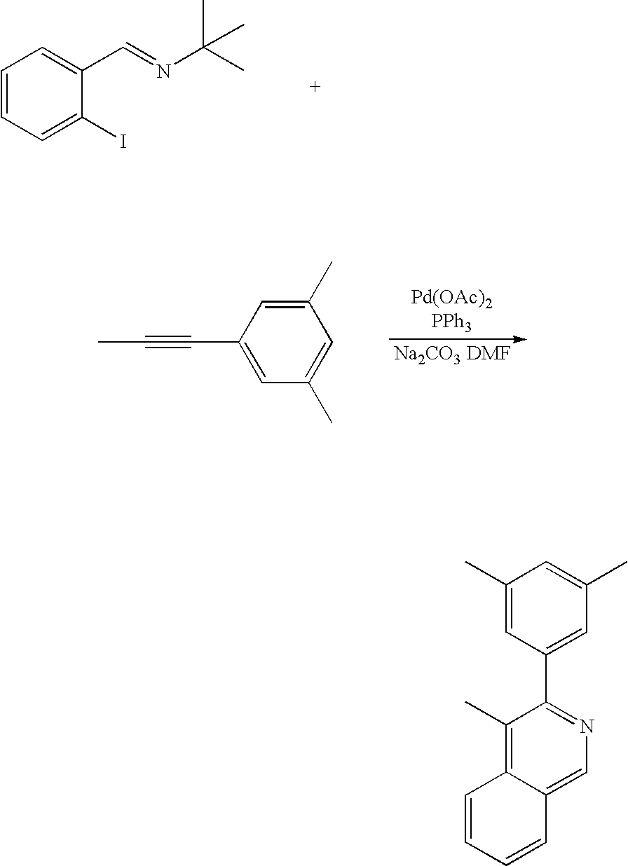
- XYGCWKZICRDGQG-QIRWAITMSA-N CC#CC1=CC(C)=CC(C)=C1.CC(C)(C)/N=C/C1=CC=CC=C1I.CC1=CC(C)=CC(C2=NC=C3C=CC=CC3=C2C)=C1 Chemical compound CC#CC1=CC(C)=CC(C)=C1.CC(C)(C)/N=C/C1=CC=CC=C1I.CC1=CC(C)=CC(C2=NC=C3C=CC=CC3=C2C)=C1 XYGCWKZICRDGQG-QIRWAITMSA-N 0.000 description 1
- LCLCVVVHIPPHCG-UHFFFAOYSA-N CC(=O)CC(=O)C(C)(C)C Chemical compound CC(=O)CC(=O)C(C)(C)C LCLCVVVHIPPHCG-UHFFFAOYSA-N 0.000 description 1
- LFWLQQJIEHWUDM-UHFFFAOYSA-N CC(=O)CC(=O)C(C)(F)F Chemical compound CC(=O)CC(=O)C(C)(F)F LFWLQQJIEHWUDM-UHFFFAOYSA-N 0.000 description 1
- YRKCREAYFQTBPV-UHFFFAOYSA-N CC(=O)CC(C)=O Chemical compound CC(=O)CC(C)=O YRKCREAYFQTBPV-UHFFFAOYSA-N 0.000 description 1
- MBZYMOPHUYVIQX-DQUMSKCSSA-M CC(=O)CC(C)=O.CC1=CC(C)=C2C(=C1)C1=N(CC3=C(=C1C)C=CC=C3)[Ir]21Cl[Ir]2(Cl1)C1=C(C=C(C)C=C1C)C1=C(C)C3=CC=CC=C3C=N12.CC1=CC2=C(C(C)=C1)[Ir]1(OC(C)=CC(C)=O1)N1=CC3=CC=CC=C3C(C)=C21 Chemical compound CC(=O)CC(C)=O.CC1=CC(C)=C2C(=C1)C1=N(CC3=C(=C1C)C=CC=C3)[Ir]21Cl[Ir]2(Cl1)C1=C(C=C(C)C=C1C)C1=C(C)C3=CC=CC=C3C=N12.CC1=CC2=C(C(C)=C1)[Ir]1(OC(C)=CC(C)=O1)N1=CC3=CC=CC=C3C(C)=C21 MBZYMOPHUYVIQX-DQUMSKCSSA-M 0.000 description 1
- PKQIDSVLSKFZQC-UHFFFAOYSA-N CC(=O)CC=O Chemical compound CC(=O)CC=O PKQIDSVLSKFZQC-UHFFFAOYSA-N 0.000 description 1
- YRAJNWYBUCUFBD-UHFFFAOYSA-N CC(C)(C)C(=O)CC(=O)C(C)(C)C Chemical compound CC(C)(C)C(=O)CC(=O)C(C)(C)C YRAJNWYBUCUFBD-UHFFFAOYSA-N 0.000 description 1
- FVRFCCHVNVOJQT-UHFFFAOYSA-N CC(F)(F)C(=O)CC(=O)C(C)(F)F Chemical compound CC(F)(F)C(=O)CC(=O)C(C)(F)F FVRFCCHVNVOJQT-UHFFFAOYSA-N 0.000 description 1
- QJXMSPKPHBLTMZ-UHFFFAOYSA-N CC1=C(C)C(C)=C(C)C(C2=C(C)C3=CC=CC=C3C=N2)=C1.CC1=CC(C)=C(C)C(C2=C(C)C3=CC=CC=C3C=N2)=C1.CC1=CC(C)=CC(C2=C(C)C3=CC=CC=C3C=N2)=C1.CC1=CC=C(C2=C(C)C3=CC=CC=C3C=N2)C(C)=C1.CC1=CC=C(C2=C(C)C3=CC=CC=C3C=N2)C=C1C Chemical compound CC1=C(C)C(C)=C(C)C(C2=C(C)C3=CC=CC=C3C=N2)=C1.CC1=CC(C)=C(C)C(C2=C(C)C3=CC=CC=C3C=N2)=C1.CC1=CC(C)=CC(C2=C(C)C3=CC=CC=C3C=N2)=C1.CC1=CC=C(C2=C(C)C3=CC=CC=C3C=N2)C(C)=C1.CC1=CC=C(C2=C(C)C3=CC=CC=C3C=N2)C=C1C QJXMSPKPHBLTMZ-UHFFFAOYSA-N 0.000 description 1
- YRUSTSQNGNQSCC-UHFFFAOYSA-N CC1=C(C)C(C2=C(C)C3=CC=CC=C3C=N2)=CC=C1.CC1=CC(C2=C(C)C3=CC=CC=C3C=N2)=CC=C1.CC1=CC=C(C)C(C2=C(C)C3=CC=CC=C3C=N2)=C1.CC1=CC=C(C2=C(C)C3=CC=CC=C3C=N2)C=C1.CC1=CC=CC=C1C1=C(C)C2=CC=CC=C2C=N1 Chemical compound CC1=C(C)C(C2=C(C)C3=CC=CC=C3C=N2)=CC=C1.CC1=CC(C2=C(C)C3=CC=CC=C3C=N2)=CC=C1.CC1=CC=C(C)C(C2=C(C)C3=CC=CC=C3C=N2)=C1.CC1=CC=C(C2=C(C)C3=CC=CC=C3C=N2)C=C1.CC1=CC=CC=C1C1=C(C)C2=CC=CC=C2C=N1 YRUSTSQNGNQSCC-UHFFFAOYSA-N 0.000 description 1
- PQUGAYFKODIXRW-IURJRJGRSA-I CC1=C(C)C2=C(C=C1)[Ir]1(OC(C(C)(C)C)=CC(C(C)(C)C)=O1)N1=CC3=CC=CC=C3C(C)=C21.CC1=CC2=C(C(C)=C1)C1=C(C)C3=CC=CC=C3C=N1[Ir]21OC(C(C)(C)C)=CC(C(C)(C)C)=O1.CC1=CC2=C(C(C)=C1)[Ir]1(OC(C(C)(C)C)=CC(C(C)(C)C)=O1)N1=CC3=CC=CC=C3C(C)=C21.CC1=CC2=C(C=C1C)[Ir]1(OC(C(C)(C)C)=CC(C(C)(C)C)=O1)N1=CC3=CC=CC=C3C(C)=C21.CC1=CC=C(C)C2=C1C1=C(C)C3=CC=CC=C3C=N1[Ir]21OC(C(C)(C)C)=CC(C(C)(C)C)=O1 Chemical compound CC1=C(C)C2=C(C=C1)[Ir]1(OC(C(C)(C)C)=CC(C(C)(C)C)=O1)N1=CC3=CC=CC=C3C(C)=C21.CC1=CC2=C(C(C)=C1)C1=C(C)C3=CC=CC=C3C=N1[Ir]21OC(C(C)(C)C)=CC(C(C)(C)C)=O1.CC1=CC2=C(C(C)=C1)[Ir]1(OC(C(C)(C)C)=CC(C(C)(C)C)=O1)N1=CC3=CC=CC=C3C(C)=C21.CC1=CC2=C(C=C1C)[Ir]1(OC(C(C)(C)C)=CC(C(C)(C)C)=O1)N1=CC3=CC=CC=C3C(C)=C21.CC1=CC=C(C)C2=C1C1=C(C)C3=CC=CC=C3C=N1[Ir]21OC(C(C)(C)C)=CC(C(C)(C)C)=O1 PQUGAYFKODIXRW-IURJRJGRSA-I 0.000 description 1
- LRYFGTVVWVFOAO-OJOPDJOJSA-J CC1=CC(C)=C(C)C2=C1C1=C(C)C3=CC=CC=C3C=N1[Ir]21OC(C(C)(C)C)=CC(C(C)(C)C)=O1.CC1=CC(C)=C(C)C2=C1[Ir]1(OC(C(C)(C)C)=CC(C(C)(C)C)=O1)N1=CC3=CC=CC=C3C(C)=C21.CC1=CC2=C(C(C)=C1C)C1=C(C)C3=CC=CC=C3C=N1[Ir]21OC(C(C)(C)C)=CC(C(C)(C)C)=O1.CC1=CC2=C(C(C)=C1C)[Ir]1(OC(C(C)(C)C)=CC(C(C)(C)C)=O1)N1=CC3=CC=CC=C3C(C)=C21 Chemical compound CC1=CC(C)=C(C)C2=C1C1=C(C)C3=CC=CC=C3C=N1[Ir]21OC(C(C)(C)C)=CC(C(C)(C)C)=O1.CC1=CC(C)=C(C)C2=C1[Ir]1(OC(C(C)(C)C)=CC(C(C)(C)C)=O1)N1=CC3=CC=CC=C3C(C)=C21.CC1=CC2=C(C(C)=C1C)C1=C(C)C3=CC=CC=C3C=N1[Ir]21OC(C(C)(C)C)=CC(C(C)(C)C)=O1.CC1=CC2=C(C(C)=C1C)[Ir]1(OC(C(C)(C)C)=CC(C(C)(C)C)=O1)N1=CC3=CC=CC=C3C(C)=C21 LRYFGTVVWVFOAO-OJOPDJOJSA-J 0.000 description 1
- WYFFKBDIRCMKBD-UHFFFAOYSA-N CC1=CC(C)=C(C)C=C1C1=C(C)C2=CC=CC=C2C=N1.CC1=CC=C(C2=C(C)C3=CC=CC=C3C=N2)C(C)=C1C Chemical compound CC1=CC(C)=C(C)C=C1C1=C(C)C2=CC=CC=C2C=N1.CC1=CC=C(C2=C(C)C3=CC=CC=C3C=N2)C(C)=C1C WYFFKBDIRCMKBD-UHFFFAOYSA-N 0.000 description 1
- XLICYMWHAWXJQI-UHFFFAOYSA-N CC1=CC(C)=C2C(=C1)C1=C(C)C3=C(C=CC=C3)C=N1[Ir]21Cl[Ir]2(Cl1)C1=C(C=C(C)C=C1C)C1=C(C)C3=CC=CC=C3C=N12.CC1=CC(C)=CC(C2=C(C)C3=CC=CC=C3C=N2)=C1 Chemical compound CC1=CC(C)=C2C(=C1)C1=C(C)C3=C(C=CC=C3)C=N1[Ir]21Cl[Ir]2(Cl1)C1=C(C=C(C)C=C1C)C1=C(C)C3=CC=CC=C3C=N12.CC1=CC(C)=CC(C2=C(C)C3=CC=CC=C3C=N2)=C1 XLICYMWHAWXJQI-UHFFFAOYSA-N 0.000 description 1
- AXXPIKVMMOBKFV-LPVWSDGXSA-I CC1=CC(C)=O[Ir]2(O1)C1=C(C(C)=CC(C)=C1C)C1=C(C)C3=CC=CC=C3C=N12.CC1=CC(C)=O[Ir]2(O1)C1=C(C=C(C)C(C)=C1C)C1=C(C)C3=CC=CC=C3C=N12.CC1=CC2=C(C=C1)C1=C(C)C3=CC=CC=C3C=N1[Ir]21OC(C(C)(C)C)=CC(C(C)(C)C)=O1.CC1=CC2=C(C=C1)[Ir]1(OC(C(C)(C)C)=CC(C(C)(C)C)=O1)N1=CC3=CC=CC=C3C(C)=C21.CC1=CC=CC2=C1C1=C(C)C3=CC=CC=C3C=N1[Ir]21OC(C(C)(C)C)=CC(C(C)(C)C)=O1 Chemical compound CC1=CC(C)=O[Ir]2(O1)C1=C(C(C)=CC(C)=C1C)C1=C(C)C3=CC=CC=C3C=N12.CC1=CC(C)=O[Ir]2(O1)C1=C(C=C(C)C(C)=C1C)C1=C(C)C3=CC=CC=C3C=N12.CC1=CC2=C(C=C1)C1=C(C)C3=CC=CC=C3C=N1[Ir]21OC(C(C)(C)C)=CC(C(C)(C)C)=O1.CC1=CC2=C(C=C1)[Ir]1(OC(C(C)(C)C)=CC(C(C)(C)C)=O1)N1=CC3=CC=CC=C3C(C)=C21.CC1=CC=CC2=C1C1=C(C)C3=CC=CC=C3C=N1[Ir]21OC(C(C)(C)C)=CC(C(C)(C)C)=O1 AXXPIKVMMOBKFV-LPVWSDGXSA-I 0.000 description 1
- DGCTVLNZTFDPDJ-UHFFFAOYSA-N CCC(=O)CC(=O)CC Chemical compound CCC(=O)CC(=O)CC DGCTVLNZTFDPDJ-UHFFFAOYSA-N 0.000 description 1
- WSMYVTOQOOLQHP-UHFFFAOYSA-N O=CCC=O Chemical compound O=CCC=O WSMYVTOQOOLQHP-UHFFFAOYSA-N 0.000 description 1
Images


Classifications
-
- C—CHEMISTRY; METALLURGY
- C09—DYES; PAINTS; POLISHES; NATURAL RESINS; ADHESIVES; COMPOSITIONS NOT OTHERWISE PROVIDED FOR; APPLICATIONS OF MATERIALS NOT OTHERWISE PROVIDED FOR
- C09K—MATERIALS FOR MISCELLANEOUS APPLICATIONS, NOT PROVIDED FOR ELSEWHERE
- C09K11/00—Luminescent, e.g. electroluminescent, chemiluminescent materials
- C09K11/06—Luminescent, e.g. electroluminescent, chemiluminescent materials containing organic luminescent materials
-
- C—CHEMISTRY; METALLURGY
- C09—DYES; PAINTS; POLISHES; NATURAL RESINS; ADHESIVES; COMPOSITIONS NOT OTHERWISE PROVIDED FOR; APPLICATIONS OF MATERIALS NOT OTHERWISE PROVIDED FOR
- C09K—MATERIALS FOR MISCELLANEOUS APPLICATIONS, NOT PROVIDED FOR ELSEWHERE
- C09K11/00—Luminescent, e.g. electroluminescent, chemiluminescent materials
- C09K11/08—Luminescent, e.g. electroluminescent, chemiluminescent materials containing inorganic luminescent materials
- C09K11/87—Luminescent, e.g. electroluminescent, chemiluminescent materials containing inorganic luminescent materials containing platina group metals
-
- H—ELECTRICITY
- H05—ELECTRIC TECHNIQUES NOT OTHERWISE PROVIDED FOR
- H05B—ELECTRIC HEATING; ELECTRIC LIGHT SOURCES NOT OTHERWISE PROVIDED FOR; CIRCUIT ARRANGEMENTS FOR ELECTRIC LIGHT SOURCES, IN GENERAL
- H05B33/00—Electroluminescent light sources
- H05B33/12—Light sources with substantially two-dimensional radiating surfaces
- H05B33/14—Light sources with substantially two-dimensional radiating surfaces characterised by the chemical or physical composition or the arrangement of the electroluminescent material, or by the simultaneous addition of the electroluminescent material in or onto the light source
-
- H—ELECTRICITY
- H10—SEMICONDUCTOR DEVICES; ELECTRIC SOLID-STATE DEVICES NOT OTHERWISE PROVIDED FOR
- H10K—ORGANIC ELECTRIC SOLID-STATE DEVICES
- H10K50/00—Organic light-emitting devices
- H10K50/10—OLEDs or polymer light-emitting diodes [PLED]
- H10K50/11—OLEDs or polymer light-emitting diodes [PLED] characterised by the electroluminescent [EL] layers
-
- H—ELECTRICITY
- H10—SEMICONDUCTOR DEVICES; ELECTRIC SOLID-STATE DEVICES NOT OTHERWISE PROVIDED FOR
- H10K—ORGANIC ELECTRIC SOLID-STATE DEVICES
- H10K85/00—Organic materials used in the body or electrodes of devices covered by this subclass
- H10K85/30—Coordination compounds
- H10K85/341—Transition metal complexes, e.g. Ru(II)polypyridine complexes
- H10K85/342—Transition metal complexes, e.g. Ru(II)polypyridine complexes comprising iridium
-
- C—CHEMISTRY; METALLURGY
- C09—DYES; PAINTS; POLISHES; NATURAL RESINS; ADHESIVES; COMPOSITIONS NOT OTHERWISE PROVIDED FOR; APPLICATIONS OF MATERIALS NOT OTHERWISE PROVIDED FOR
- C09K—MATERIALS FOR MISCELLANEOUS APPLICATIONS, NOT PROVIDED FOR ELSEWHERE
- C09K2211/00—Chemical nature of organic luminescent or tenebrescent compounds
- C09K2211/10—Non-macromolecular compounds
- C09K2211/1018—Heterocyclic compounds
- C09K2211/1025—Heterocyclic compounds characterised by ligands
- C09K2211/1029—Heterocyclic compounds characterised by ligands containing one nitrogen atom as the heteroatom
-
- C—CHEMISTRY; METALLURGY
- C09—DYES; PAINTS; POLISHES; NATURAL RESINS; ADHESIVES; COMPOSITIONS NOT OTHERWISE PROVIDED FOR; APPLICATIONS OF MATERIALS NOT OTHERWISE PROVIDED FOR
- C09K—MATERIALS FOR MISCELLANEOUS APPLICATIONS, NOT PROVIDED FOR ELSEWHERE
- C09K2211/00—Chemical nature of organic luminescent or tenebrescent compounds
- C09K2211/10—Non-macromolecular compounds
- C09K2211/1018—Heterocyclic compounds
- C09K2211/1025—Heterocyclic compounds characterised by ligands
- C09K2211/1092—Heterocyclic compounds characterised by ligands containing sulfur as the only heteroatom
-
- C—CHEMISTRY; METALLURGY
- C09—DYES; PAINTS; POLISHES; NATURAL RESINS; ADHESIVES; COMPOSITIONS NOT OTHERWISE PROVIDED FOR; APPLICATIONS OF MATERIALS NOT OTHERWISE PROVIDED FOR
- C09K—MATERIALS FOR MISCELLANEOUS APPLICATIONS, NOT PROVIDED FOR ELSEWHERE
- C09K2211/00—Chemical nature of organic luminescent or tenebrescent compounds
- C09K2211/18—Metal complexes
- C09K2211/185—Metal complexes of the platinum group, i.e. Os, Ir, Pt, Ru, Rh or Pd
-
- H—ELECTRICITY
- H10—SEMICONDUCTOR DEVICES; ELECTRIC SOLID-STATE DEVICES NOT OTHERWISE PROVIDED FOR
- H10K—ORGANIC ELECTRIC SOLID-STATE DEVICES
- H10K2101/00—Properties of the organic materials covered by group H10K85/00
- H10K2101/10—Triplet emission
-
- H—ELECTRICITY
- H10—SEMICONDUCTOR DEVICES; ELECTRIC SOLID-STATE DEVICES NOT OTHERWISE PROVIDED FOR
- H10K—ORGANIC ELECTRIC SOLID-STATE DEVICES
- H10K85/00—Organic materials used in the body or electrodes of devices covered by this subclass
- H10K85/30—Coordination compounds
- H10K85/321—Metal complexes comprising a group IIIA element, e.g. Tris (8-hydroxyquinoline) gallium [Gaq3]
- H10K85/324—Metal complexes comprising a group IIIA element, e.g. Tris (8-hydroxyquinoline) gallium [Gaq3] comprising aluminium, e.g. Alq3
-
- Y—GENERAL TAGGING OF NEW TECHNOLOGICAL DEVELOPMENTS; GENERAL TAGGING OF CROSS-SECTIONAL TECHNOLOGIES SPANNING OVER SEVERAL SECTIONS OF THE IPC; TECHNICAL SUBJECTS COVERED BY FORMER USPC CROSS-REFERENCE ART COLLECTIONS [XRACs] AND DIGESTS
- Y10—TECHNICAL SUBJECTS COVERED BY FORMER USPC
- Y10S—TECHNICAL SUBJECTS COVERED BY FORMER USPC CROSS-REFERENCE ART COLLECTIONS [XRACs] AND DIGESTS
- Y10S428/00—Stock material or miscellaneous articles
- Y10S428/917—Electroluminescent
Definitions
- the present invention relates to a red light-emitting phosphorescent compound (hereinafter, referred to simply to as a ‘red phosphorescent compound’) and an organic electroluminescent (EL) device using the same. More particularly, the present invention relates to a red phosphorescent compound and an organic electroluminescent device realizing an improvement in color purity by using the red phosphorescent compound as a dopant of a light-emitting layer.
- a red phosphorescent compound hereinafter, referred to simply to as a ‘red phosphorescent compound’
- EL organic electroluminescent
- electroluminescent devices are self-luminous display devices, they have the advantages of a wide viewing angle, a large contrast ratio, and a high response speed. Electroluminescent devices are divided into inorganic electroluminescent devices and organic electroluminescent devices depending upon the kind of the material for a light-emitting layer. Organic electroluminescent devices have advantages of high luminescence, low operation voltage, high response speed, and superior multi-color representation, as compared to inorganic electroluminescent devices.
- Organic electroluminescent devices When charge carriers are injected into an organic light-emitting layer formed between an electron injecting electrode (cathode) and a hole injecting electrode (anode) of an organic electroluminescent device, electrons combine with holes to create electron-hole pairs, which then decay to emit light.
- Organic electroluminescent devices have advantages in that they can be fabricated on flexible transparent substrates (e.g., plastic substrates) and can be operated at a voltage (e.g., 10V or below) lower than voltages required to operate plasma display panels (PDPs) and inorganic electroluminescent devices. Other advantages of organic electroluminescent devices are relatively low power consumption and excellent color representation.
- organic electroluminescent (EL) devices can emit light of three colors (i.e., green, blue and red), they have been the focus of intense interest lately as next-generation display devices capable of producing images of various colors.
- a general method for fabricating organic EL devices will be briefly explained below.
- a transparent substrate is covered with an anode material.
- Indium tin oxide (ITO) is generally used as the anode material.
- a hole injecting layer (HIL) is laminated to a thickness of 10 to 30 nm on the anode.
- Copper (II) phthalocyanine (CuPc) is mainly used as a material of the hole injecting layer.
- a hole transport layer is formed by depositing 4,4′-bis[N-(1-naphthyl)-N-phenylamino]-biphenyl (NPB) to a thickness of about 30 to about 60 nm on the hole injecting layer.
- An organic light-emitting layer is formed on the hole transport layer. If necessary, a dopant may be added to a material for the organic light-emitting layer.
- a dopant may be added to a material for the organic light-emitting layer.
- tris(8-hydroxyquinoline)aluminum (Alq 3 ) as a material for the organic light-emitting layer is deposited to a thickness of about 30 to about 60 nm on the hole transport layer, and N-methylquinacridone (MQD) is mainly used as the dopant.
- An electron transport layer (ETL) and an electron injecting layer (EIL) are sequentially laminated on the organic light-emitting layer.
- an electron injecting/transport layer is laminated on the organic light-emitting layer.
- Alq 3 has excellent electron-transport ability, the formation of the electron injecting/transport layer may be unnecessary.
- a cathode is deposited on the electron injecting layer, and finally a passivation film is covered thereon.
- the type of the organic electroluminescent devices i.e. blue, green and red light-emitting devices
- the type of the organic electroluminescent devices i.e. blue, green and red light-emitting devices
- Phosphorescent materials for use in organic EL devices must satisfy the requirements of high luminescence efficiency, high color purity and long luminescence lifetime. As shown in FIG. 1 , as the color purity of an organic EL device using a red phosphorescent material becomes higher (i.e. as the x-values on CIE chromaticity coordinates increase), the spectral luminous efficacy of the organic EL device decreases, making it difficult to achieve high luminescence efficiency of the organic EL device.
- the present invention is directed to a red phosphorescent compound and an organic electroluminescent (EL) device using the same that substantially obviate one or more problems due to limitations and disadvantages of the related art.
- An object of the present invention is to provide a red phosphorescent compound that exhibits desirable chromaticity coordinate characteristics (CIE color purity X>0.65), high luminescence efficiency, and long luminescence lifetime.
- Another object of the present invention is to provide an organic electroluminescent (EL) device using the red phosphorescent compound.
- R1 is selected from the group consisting of C 1 -C 4 alkyl and C 1 -C 4 alkoxy;
- R2, R3, R4 and R5 are independently selected from the group consisting of hydrogen, C 1 -C 4 alkyl and C 1 -C 4 alkoxy;
- an organic electroluminescent (EL) device comprising a light-emitting layer wherein the red phosphorescent compound of Formula 1 is used as a dopant for the light-emitting layer.
- an organic electroluminescent (EL) device comprising a first electrode, a light-emitting layer using a red phosphorescent compound as a dopant, and a second electrode, and exhibiting a luminescence of 1,300 to 1,450 cd/m 2 at an electric current of 0.8 to 1 mA and an applied voltage of 5.7 to 6.1 V.
- FIG. 1 shows a graph showing a phenomenon wherein the color purity of an organic EL device becomes higher (i.e. as the x-values on CIE chromaticity coordinates increase), the relative spectral sensitivity of the organic EL device decreases;
- FIG. 2 shows the structural formulas of NPB, copper (II) phthalocyanine (CuPc), (btp) 2 Ir(acac), Alq 3 , BAlq, and CBP used in one embodiment of the red phosphorescent compound according to the present invention.
- the present invention provides a red phosphorescent compound of Formula 1:
- R1 is selected from the group consisting of C 1 -C 4 alkyl and C 1 -C 4 alkoxy;
- R2, R3, R4 and R5 are independently selected from the group consisting of hydrogen, C 1 -C 4 alkyl and C 1 -C 4 alkoxy;
- Examples of preferred compounds that can be represented by Formula 1 include the following compounds:
- the present invention provides an organic electroluminescent (EL) device comprising an organic light-emitting layer wherein the red phosphorescent compound of Formula 1 is used as a dopant for the organic light-emitting layer.
- EL organic electroluminescent
- a host used in the organic light-emitting layer of the organic EL device according to the present invention may be selected from Al complexes, Zn complexes, and carbazole derivatives.
- the red phosphorescent compound of Formula 1 may be used as the dopant in an amount of 0.5 to 20% by weight. When the dopant is used within this range, improvements in chromaticity coordinate characteristics (CIE color purity X ⁇ 0.65), high luminescence efficiency, and long luminescence lifetime of the organic EL device can be realized.
- the Al and Zn complexes may have at least one ligand selected from the group consisting of quinol, biphenyl, isoquinol, phenyl, methylquinol, dimethylquinol and dimethylisoquinol.
- the carbazole derivatives may be preferably 4,4′-N,N′ dicarbazole biphenyl (CBP).
- A-7 iridium (III) (3-(3,5-dimethylphenyl)-4-methylisoquinolinato-N,C 2′ )(2,4-pentanedionate-O,O) (“A-7”), which is a red phosphorescent compound represented by Formula 1 according to the present invention.
- the dichloro-crosslinked dimer complex (1 mmol), 2,4-pentanedione (3 mmol), Na 2 CO 3 (6 mmol) and 2-ethoxyethanol (30 mL) were put in a dried two-neck round-bottom flask. Then, the mixture was refluxed for 24 hours. After the temperature was allowed to room temperature, distilled water was added thereto to obtain a solid. The solid was filtered and dissolved in dichloromethane. The solution was filtered through silica gel. The solvent was distilled off under reduced pressure and the residue was washed with methanol and petroleum ether to yield the compound.
- the examples relate to an organic electroluminescent (EL) device comprising an organic light-emitting layer which uses the red phosphorescent compound of Formula 1 as a dopant.
- the invention is not to be construed as being limited to the examples.
- An ITO-coated glass substrate was patterned to have a light-emitting area of 3 mm ⁇ 3 mm, followed by cleaning. After the patterned substrate was disposed in a vacuum chamber, the standard pressure of the chamber was adjusted to 1 ⁇ 10 ⁇ 6 torr. CuPc (200 ⁇ ), NPD (400 ⁇ ), BAlq+A-1 (7%) (200 ⁇ ), Alq 3 (300 ⁇ ), LiF (5 ⁇ ) and Al (1,000 ⁇ ) were sequentially deposited on the ITO glass substrate to fabricate an organic EL device.
- the lifetime (defined as the time taken before the luminance of the organic EL device decreases to half its initial value) of the organic EL device was 3,700 hours at 2,000 cd/m 2 .
- An ITO-coated glass substrate was patterned to have a light-emitting area of 3 mm ⁇ 3 mm, followed by cleaning. After the patterned substrate was disposed in a vacuum chamber, the standard pressure of the chamber was adjusted to 1 ⁇ 10 ⁇ 6 torr. CuPc (200 ⁇ ), NPD (400 ⁇ ), BAlq+A-2 (7%) (200 ⁇ ), Alq 3 (300 ⁇ ), LiF (5 ⁇ ) and Al (1,000 ⁇ ) were sequentially deposited on the ITO glass substrate to fabricate an organic EL device.
- the lifetime (defined as the time taken before the luminance of the organic EL device decreases to half its initial value) of the organic EL device was 4,200 hours at 2,000 cd/m 2 .
- An ITO-coated glass substrate was patterned to have a light-emitting area of 3 mm ⁇ 3 mm, followed by cleaning. After the patterned substrate was disposed in a vacuum chamber, the standard pressure of the chamber was adjusted to 1 ⁇ 10 ⁇ 6 torr. CuPc (200 ⁇ ), NPD (400 ⁇ ), BAlq+A-4 (7%) (200 ⁇ ), Alq 3 (300 ⁇ ), LiF (5 ⁇ ) and Al (1,000 ⁇ ) were sequentially deposited on the ITO glass substrate to fabricate an organic EL device.
- the lifetime (defined as the time taken before the luminance of the organic EL device decreases to half its initial value) of the organic EL device was 4,000 hours at 2,000 cd/m 2 .
- An ITO-coated glass substrate was patterned to have a light-emitting area of 3 mm ⁇ 3 mm, followed by cleaning.
- the patterned substrate was disposed in a vacuum chamber. Then, the standard pressure of the chamber was adjusted to 1 ⁇ 10 ⁇ 6 torr.
- CuPc (200 ⁇ ), NPD (400 ⁇ ), BAlq+A-7 (7%) (200 ⁇ ), Alq 3 (300 ⁇ ), LiF (5 ⁇ ) and Al (1,000 ⁇ ) were sequentially deposited on the ITO glass substrate to fabricate an organic EL device.
- the lifetime (defined as the time taken before the luminance of the organic EL device decreases to half its initial value) of the organic EL device was 4,100 hours at 2,000 cd/m 2 .
- An ITO-coated glass substrate was patterned to have a light-emitting area of 3 mm ⁇ 3 mm, followed by cleaning.
- the patterned substrate was disposed in a vacuum chamber. Then, the standard pressure of the chamber was adjusted to 1 ⁇ 10 ⁇ 6 torr.
- CuPc (200 ⁇ ), NPD (400 ⁇ ), BAlq+(btp) 2 Ir (acac) (7%) (200 ⁇ ), Alq 3 (300 ⁇ ), LiF (5 ⁇ ) and Al (1,000 ⁇ ) were sequentially deposited on the ITO glass substrate to fabricate an organic EL device.
- the lifetime (defined as the time taken before the luminance of the organic EL device decreases to half its initial value) of the organic EL device was 2,500 hours at 2,000 cd/m 2 .
- the organic EL devices fabricated in Examples 1 to 4 comprise a light-emitting layer which uses the red phosphorescent compound of Formula 1 as a dopant.
- a voltage of 5.7 to 6.1 V is applied to the organic EL device, the electric current of the organic EL device was 0.8 to 1 mA, and the luminance of the organic EL was 1,300 to 1,450 cd/m 2 .
- the electric current of 0.8 to 1 mA corresponds to a current density of 8 to 10 mA/cm 2 .
- the organic EL device exhibited a lifetime of 3,500 to 4,500. The lifetime is defined as the time taken before the luminance of the organic EL device decreases to half its initial value.
- the organic EL device had a current efficiency of 10 to 15 cd/A and a power efficiency of 6 to 8 Im/W.
- the red phosphorescent compound of Formula 1 is used as a dopant for the light-emitting layer.
- EL organic electroluminescent
Abstract

-
- wherein
-
- is

and R1, R2, R3, R4 and R5 are as defined in the specification.
Description

is

R1 is selected from the group consisting of C1-C4 alkyl and C1-C4 alkoxy; R2, R3, R4 and R5 are independently selected from the group consisting of hydrogen, C1-C4 alkyl and C1-C4 alkoxy; and
is selected from the group consisting of 2,4-pentanedione, 2,2,6,6,-tetramethylheptane-3,5-dione, 1,3-propanedione, 1,3-butanedione, 3,5-heptanedione, 1,1,1-trifluoro-2,4-pentanedione, 1,1,1,5,5,5-hexafluoro-2,4-pentanedione, and 2,2-dimethyl-3,5-hexanedione.

is

R1 is selected from the group consisting of C1-C4 alkyl and C1-C4 alkoxy; R2, R3, R4 and R5 are independently selected from the group consisting of hydrogen, C1-C4 alkyl and C1-C4 alkoxy; and
is selected from the group consisting of 2,4-pentanedione
2,2,6,6,-tetramethylheptane-3,5-dione

1,3
propanedione
1,3-butanedione
3,5-heptanedione
1,1,1-trifluoro-2,4-pentanedione

1,1,1,5,5,5-hexafluoro-2,4-pentanedione

and 2,2-dimethyl-3,5-hexanedione

in Formula 1 is selected from the following compounds:


| TABLE 1 | ||||||||
| Life time (h) | ||||||||
| Electric | Current | Power | (half the | |||||
| Voltage | current | Luminance | efficiency | efficiency | CIE | CIE | initial | |
| Device | (V) | (mA) | (cd/m2) | (cd/A) | (lm/W) | (X) | (Y) | luminance) |
| Ex. 1 | 6.1 | 0.9 | 1326 | 13.26 | 6.83 | 0.601 | 0.327 | 3700 |
| Ex. 2 | 5.7 | 0.9 | 1420 | 14.20 | 7.82 | 0.592 | 0.330 | 4200 |
| Ex. 3 | 5.8 | 0.9 | 1411 | 14.11 | 7.64 | 0.621 | 0.336 | 4000 |
| Ex. 4 | 5.7 | 0.9 | 1350 | 13.50 | 7.44 | 0.610 | 0.329 | 4100 |
| Comp. Ex. | 7.5 | 0.9 | 780 | 7.8 | 3.3 | 0.659 | 0.329 | 2500 |
Claims (7)


Applications Claiming Priority (2)
| Application Number | Priority Date | Filing Date | Title |
|---|---|---|---|
| KR1020060026630A KR20070097139A (en) | 2006-03-23 | 2006-03-23 | Red phosphorescene compounds and organic electroluminescence devices using the same |
| KR10-2006-0026630 | 2006-03-23 |
Publications (2)
| Publication Number | Publication Date |
|---|---|
| US20070224450A1 US20070224450A1 (en) | 2007-09-27 |
| US8623519B2 true US8623519B2 (en) | 2014-01-07 |
Family
ID=38533830
Family Applications (1)
| Application Number | Title | Priority Date | Filing Date |
|---|---|---|---|
| US11/723,887 Active 2030-06-03 US8623519B2 (en) | 2006-03-23 | 2007-03-22 | Red phosphorescent compound and organic electroluminescent device using the same |
Country Status (2)
| Country | Link |
|---|---|
| US (1) | US8623519B2 (en) |
| KR (1) | KR20070097139A (en) |
Families Citing this family (69)
| Publication number | Priority date | Publication date | Assignee | Title |
|---|---|---|---|---|
| US9130177B2 (en) | 2011-01-13 | 2015-09-08 | Universal Display Corporation | 5-substituted 2 phenylquinoline complexes materials for light emitting diode |
| US10008677B2 (en) | 2011-01-13 | 2018-06-26 | Universal Display Corporation | Materials for organic light emitting diode |
| KR102120890B1 (en) * | 2012-11-01 | 2020-06-10 | 삼성디스플레이 주식회사 | Heterocyclic compound and organic light emitting diode comprising the same |
| US10199581B2 (en) | 2013-07-01 | 2019-02-05 | Universal Display Corporation | Organic electroluminescent materials and devices |
| US10749118B2 (en) | 2014-06-26 | 2020-08-18 | Samsung Display Co., Ltd. | Heterocyclic compound and organic light-emitting device including the same |
| US9929361B2 (en) | 2015-02-16 | 2018-03-27 | Universal Display Corporation | Organic electroluminescent materials and devices |
| US11056657B2 (en) | 2015-02-27 | 2021-07-06 | University Display Corporation | Organic electroluminescent materials and devices |
| US9859510B2 (en) | 2015-05-15 | 2018-01-02 | Universal Display Corporation | Organic electroluminescent materials and devices |
| US10418568B2 (en) | 2015-06-01 | 2019-09-17 | Universal Display Corporation | Organic electroluminescent materials and devices |
| US11127905B2 (en) | 2015-07-29 | 2021-09-21 | Universal Display Corporation | Organic electroluminescent materials and devices |
| US10672996B2 (en) | 2015-09-03 | 2020-06-02 | Universal Display Corporation | Organic electroluminescent materials and devices |
| US20170229663A1 (en) | 2016-02-09 | 2017-08-10 | Universal Display Corporation | Organic electroluminescent materials and devices |
| US10236456B2 (en) | 2016-04-11 | 2019-03-19 | Universal Display Corporation | Organic electroluminescent materials and devices |
| US11482683B2 (en) | 2016-06-20 | 2022-10-25 | Universal Display Corporation | Organic electroluminescent materials and devices |
| US10862054B2 (en) | 2016-06-20 | 2020-12-08 | Universal Display Corporation | Organic electroluminescent materials and devices |
| US10672997B2 (en) | 2016-06-20 | 2020-06-02 | Universal Display Corporation | Organic electroluminescent materials and devices |
| US10608186B2 (en) | 2016-09-14 | 2020-03-31 | Universal Display Corporation | Organic electroluminescent materials and devices |
| US10680187B2 (en) | 2016-09-23 | 2020-06-09 | Universal Display Corporation | Organic electroluminescent materials and devices |
| US11196010B2 (en) | 2016-10-03 | 2021-12-07 | Universal Display Corporation | Organic electroluminescent materials and devices |
| US11011709B2 (en) | 2016-10-07 | 2021-05-18 | Universal Display Corporation | Organic electroluminescent materials and devices |
| US20180130956A1 (en) | 2016-11-09 | 2018-05-10 | Universal Display Corporation | Organic electroluminescent materials and devices |
| US10680188B2 (en) | 2016-11-11 | 2020-06-09 | Universal Display Corporation | Organic electroluminescent materials and devices |
| US11780865B2 (en) | 2017-01-09 | 2023-10-10 | Universal Display Corporation | Organic electroluminescent materials and devices |
| US10844085B2 (en) | 2017-03-29 | 2020-11-24 | Universal Display Corporation | Organic electroluminescent materials and devices |
| US10944060B2 (en) | 2017-05-11 | 2021-03-09 | Universal Display Corporation | Organic electroluminescent materials and devices |
| US20180370999A1 (en) | 2017-06-23 | 2018-12-27 | Universal Display Corporation | Organic electroluminescent materials and devices |
| US11228010B2 (en) | 2017-07-26 | 2022-01-18 | Universal Display Corporation | Organic electroluminescent materials and devices |
| US11744142B2 (en) | 2017-08-10 | 2023-08-29 | Universal Display Corporation | Organic electroluminescent materials and devices |
| US20190161504A1 (en) | 2017-11-28 | 2019-05-30 | University Of Southern California | Carbene compounds and organic electroluminescent devices |
| EP3492480B1 (en) | 2017-11-29 | 2021-10-20 | Universal Display Corporation | Organic electroluminescent materials and devices |
| US11937503B2 (en) | 2017-11-30 | 2024-03-19 | Universal Display Corporation | Organic electroluminescent materials and devices |
| CN108191916A (en) * | 2017-12-29 | 2018-06-22 | 瑞声科技(新加坡)有限公司 | A kind of organometallic complex and luminescent device |
| US11542289B2 (en) | 2018-01-26 | 2023-01-03 | Universal Display Corporation | Organic electroluminescent materials and devices |
| US20200075870A1 (en) | 2018-08-22 | 2020-03-05 | Universal Display Corporation | Organic electroluminescent materials and devices |
| US11737349B2 (en) | 2018-12-12 | 2023-08-22 | Universal Display Corporation | Organic electroluminescent materials and devices |
| US11780829B2 (en) | 2019-01-30 | 2023-10-10 | The University Of Southern California | Organic electroluminescent materials and devices |
| US20200251664A1 (en) | 2019-02-01 | 2020-08-06 | Universal Display Corporation | Organic electroluminescent materials and devices |
| JP2020158491A (en) | 2019-03-26 | 2020-10-01 | ユニバーサル ディスプレイ コーポレイション | Organic electroluminescent materials and devices |
| US20210032278A1 (en) | 2019-07-30 | 2021-02-04 | Universal Display Corporation | Organic electroluminescent materials and devices |
| US20210047354A1 (en) | 2019-08-16 | 2021-02-18 | Universal Display Corporation | Organic electroluminescent materials and devices |
| US20210135130A1 (en) | 2019-11-04 | 2021-05-06 | Universal Display Corporation | Organic electroluminescent materials and devices |
| US20210217969A1 (en) | 2020-01-06 | 2021-07-15 | Universal Display Corporation | Organic electroluminescent materials and devices |
| US20220336759A1 (en) | 2020-01-28 | 2022-10-20 | Universal Display Corporation | Organic electroluminescent materials and devices |
| EP3937268A1 (en) | 2020-07-10 | 2022-01-12 | Universal Display Corporation | Plasmonic oleds and vertical dipole emitters |
| CN116368957A (en) | 2020-09-18 | 2023-06-30 | 三星显示有限公司 | Organic electroluminescent device |
| US20220158096A1 (en) | 2020-11-16 | 2022-05-19 | Universal Display Corporation | Organic electroluminescent materials and devices |
| US20220162243A1 (en) | 2020-11-24 | 2022-05-26 | Universal Display Corporation | Organic electroluminescent materials and devices |
| US20220165967A1 (en) | 2020-11-24 | 2022-05-26 | Universal Display Corporation | Organic electroluminescent materials and devices |
| US20220271241A1 (en) | 2021-02-03 | 2022-08-25 | Universal Display Corporation | Organic electroluminescent materials and devices |
| EP4059915A3 (en) | 2021-02-26 | 2022-12-28 | Universal Display Corporation | Organic electroluminescent materials and devices |
| EP4060758A3 (en) | 2021-02-26 | 2023-03-29 | Universal Display Corporation | Organic electroluminescent materials and devices |
| US20220298192A1 (en) | 2021-03-05 | 2022-09-22 | Universal Display Corporation | Organic electroluminescent materials and devices |
| US20220298190A1 (en) | 2021-03-12 | 2022-09-22 | Universal Display Corporation | Organic electroluminescent materials and devices |
| US20220298193A1 (en) | 2021-03-15 | 2022-09-22 | Universal Display Corporation | Organic electroluminescent materials and devices |
| US20220340607A1 (en) | 2021-04-05 | 2022-10-27 | Universal Display Corporation | Organic electroluminescent materials and devices |
| EP4075531A1 (en) | 2021-04-13 | 2022-10-19 | Universal Display Corporation | Plasmonic oleds and vertical dipole emitters |
| US20220352478A1 (en) | 2021-04-14 | 2022-11-03 | Universal Display Corporation | Organic eletroluminescent materials and devices |
| US20230006149A1 (en) | 2021-04-23 | 2023-01-05 | Universal Display Corporation | Organic electroluminescent materials and devices |
| US20220407020A1 (en) | 2021-04-23 | 2022-12-22 | Universal Display Corporation | Organic electroluminescent materials and devices |
| US20230133787A1 (en) | 2021-06-08 | 2023-05-04 | University Of Southern California | Molecular Alignment of Homoleptic Iridium Phosphors |
| EP4151699A1 (en) | 2021-09-17 | 2023-03-22 | Universal Display Corporation | Organic electroluminescent materials and devices |
| EP4212539A1 (en) | 2021-12-16 | 2023-07-19 | Universal Display Corporation | Organic electroluminescent materials and devices |
| EP4231804A3 (en) | 2022-02-16 | 2023-09-20 | Universal Display Corporation | Organic electroluminescent materials and devices |
| US20230292592A1 (en) | 2022-03-09 | 2023-09-14 | Universal Display Corporation | Organic electroluminescent materials and devices |
| US20230337516A1 (en) | 2022-04-18 | 2023-10-19 | Universal Display Corporation | Organic electroluminescent materials and devices |
| US20230389421A1 (en) | 2022-05-24 | 2023-11-30 | Universal Display Corporation | Organic electroluminescent materials and devices |
| EP4293001A1 (en) | 2022-06-08 | 2023-12-20 | Universal Display Corporation | Organic electroluminescent materials and devices |
| US20240016051A1 (en) | 2022-06-28 | 2024-01-11 | Universal Display Corporation | Organic electroluminescent materials and devices |
| US20240107880A1 (en) | 2022-08-17 | 2024-03-28 | Universal Display Corporation | Organic electroluminescent materials and devices |
Citations (5)
| Publication number | Priority date | Publication date | Assignee | Title |
|---|---|---|---|---|
| US20010019782A1 (en) * | 1999-12-27 | 2001-09-06 | Tatsuya Igarashi | Light-emitting material comprising orthometalated iridium complex, light-emitting device, high efficiency red light-emitting device, and novel iridium complex |
| US20030072964A1 (en) * | 2001-10-17 | 2003-04-17 | Kwong Raymond C. | Phosphorescent compounds and devices comprising the same |
| US20030096138A1 (en) * | 2001-11-07 | 2003-05-22 | Lecloux Daniel David | Electroluminescent iridium compounds having red-orange or red emission and devices made with such compounds |
| US20040140758A1 (en) * | 2003-01-17 | 2004-07-22 | Eastman Kodak Company | Organic light emitting device (OLED) display with improved light emission using a metallic anode |
| US20050084707A1 (en) * | 2002-02-21 | 2005-04-21 | Makoto Satsuki | Organic electroluminescence device |
-
2006
- 2006-03-23 KR KR1020060026630A patent/KR20070097139A/en active Search and Examination
-
2007
- 2007-03-22 US US11/723,887 patent/US8623519B2/en active Active
Patent Citations (5)
| Publication number | Priority date | Publication date | Assignee | Title |
|---|---|---|---|---|
| US20010019782A1 (en) * | 1999-12-27 | 2001-09-06 | Tatsuya Igarashi | Light-emitting material comprising orthometalated iridium complex, light-emitting device, high efficiency red light-emitting device, and novel iridium complex |
| US20030072964A1 (en) * | 2001-10-17 | 2003-04-17 | Kwong Raymond C. | Phosphorescent compounds and devices comprising the same |
| US20030096138A1 (en) * | 2001-11-07 | 2003-05-22 | Lecloux Daniel David | Electroluminescent iridium compounds having red-orange or red emission and devices made with such compounds |
| US20050084707A1 (en) * | 2002-02-21 | 2005-04-21 | Makoto Satsuki | Organic electroluminescence device |
| US20040140758A1 (en) * | 2003-01-17 | 2004-07-22 | Eastman Kodak Company | Organic light emitting device (OLED) display with improved light emission using a metallic anode |
Also Published As
| Publication number | Publication date |
|---|---|
| US20070224450A1 (en) | 2007-09-27 |
| KR20070097139A (en) | 2007-10-04 |
Similar Documents
| Publication | Publication Date | Title |
|---|---|---|
| US8623519B2 (en) | Red phosphorescent compound and organic electroluminescent device using the same | |
| US8530059B2 (en) | Red phosphorescent compound and organic electroluminescent device using the same | |
| US9023489B2 (en) | Red phosphorescent compounds and organic electroluminescent devices using the same | |
| US8956737B2 (en) | Red phosphorescent compound and organic electroluminescent device using the same | |
| US7470928B2 (en) | Red phosphorescence compounds | |
| US7740957B2 (en) | Red phosphorescence compounds and organic electroluminescence device using the same | |
| US8501328B2 (en) | Red phosphorescent compounds and organic electroluminescent devices using the same | |
| US9324958B2 (en) | Red phosphorescent composition and organic electroluminescent device using the same | |
| US8999476B2 (en) | Red phosphorescent composition and organic electroluminescent device using the same | |
| US8227801B2 (en) | Bicarbzole containing compounds for OLEDs | |
| US8071226B2 (en) | Red phosphorescent compounds and organic electroluminescent devices using the same | |
| TW202010745A (en) | Metal complex comprising novel ligand structures | |
| KR101555155B1 (en) | Novel spyrobifluorene type organic compounds and an organic electroluminescent device comprising the same | |
| KR20140060974A (en) | Phosphorescent material and organic light emitting diode device using the same | |
| KR100662430B1 (en) | Red phosphorescene compounds and organic electroluminescence devices using the same | |
| KR100747572B1 (en) | Red phosphorescene compounds and organic electroluminescence devices using the same | |
| KR20070105079A (en) | Red phosphorescene compounds and organic electroluminescence devices using the same | |
| KR20070097138A (en) | Red phosphorescene compounds and organic electroluminescence devices using the same |
Legal Events
| Date | Code | Title | Description |
|---|---|---|---|
| AS | Assignment |
Owner name: LG ELECTRONICS INC., KOREA, REPUBLIC OF Free format text: ASSIGNMENT OF ASSIGNORS INTEREST;ASSIGNORS:KIM, JUNG KEUN;SEO, JEONG DAE;LEE, KYUNG HOON;AND OTHERS;REEL/FRAME:019220/0328 Effective date: 20070322 |
|
| AS | Assignment |
Owner name: LG DISPLAY CO., LTD., KOREA, REPUBLIC OF Free format text: ASSIGNMENT OF ASSIGNORS INTEREST;ASSIGNOR:LG ELECTRONICS INC.;REEL/FRAME:021090/0886 Effective date: 20080404 Owner name: LG DISPLAY CO., LTD.,KOREA, REPUBLIC OF Free format text: ASSIGNMENT OF ASSIGNORS INTEREST;ASSIGNOR:LG ELECTRONICS INC.;REEL/FRAME:021090/0886 Effective date: 20080404 |
|
| FEPP | Fee payment procedure |
Free format text: PAYOR NUMBER ASSIGNED (ORIGINAL EVENT CODE: ASPN); ENTITY STATUS OF PATENT OWNER: LARGE ENTITY |
|
| STCF | Information on status: patent grant |
Free format text: PATENTED CASE |
|
| FPAY | Fee payment |
Year of fee payment: 4 |
|
| MAFP | Maintenance fee payment |
Free format text: PAYMENT OF MAINTENANCE FEE, 8TH YEAR, LARGE ENTITY (ORIGINAL EVENT CODE: M1552); ENTITY STATUS OF PATENT OWNER: LARGE ENTITY Year of fee payment: 8 |