US8618581B2 - Nanofludic field effect transistor based on surface charge modulated nanochannel - Google Patents
Nanofludic field effect transistor based on surface charge modulated nanochannel Download PDFInfo
- Publication number
- US8618581B2 US8618581B2 US13/365,577 US201213365577A US8618581B2 US 8618581 B2 US8618581 B2 US 8618581B2 US 201213365577 A US201213365577 A US 201213365577A US 8618581 B2 US8618581 B2 US 8618581B2
- Authority
- US
- United States
- Prior art keywords
- ionic
- nanochannel
- membrane
- insulating layers
- electrically conductive
- Prior art date
- Legal status (The legal status is an assumption and is not a legal conclusion. Google has not performed a legal analysis and makes no representation as to the accuracy of the status listed.)
- Active, expires
Links
Images


Classifications
-
- B—PERFORMING OPERATIONS; TRANSPORTING
- B82—NANOTECHNOLOGY
- B82Y—SPECIFIC USES OR APPLICATIONS OF NANOSTRUCTURES; MEASUREMENT OR ANALYSIS OF NANOSTRUCTURES; MANUFACTURE OR TREATMENT OF NANOSTRUCTURES
- B82Y10/00—Nanotechnology for information processing, storage or transmission, e.g. quantum computing or single electron logic
-
- G—PHYSICS
- G01—MEASURING; TESTING
- G01N—INVESTIGATING OR ANALYSING MATERIALS BY DETERMINING THEIR CHEMICAL OR PHYSICAL PROPERTIES
- G01N27/00—Investigating or analysing materials by the use of electric, electrochemical, or magnetic means
- G01N27/26—Investigating or analysing materials by the use of electric, electrochemical, or magnetic means by investigating electrochemical variables; by using electrolysis or electrophoresis
- G01N27/403—Cells and electrode assemblies
- G01N27/414—Ion-sensitive or chemical field-effect transistors, i.e. ISFETS or CHEMFETS
- G01N27/4148—Integrated circuits therefor, e.g. fabricated by CMOS processing
-
- G—PHYSICS
- G01—MEASURING; TESTING
- G01N—INVESTIGATING OR ANALYSING MATERIALS BY DETERMINING THEIR CHEMICAL OR PHYSICAL PROPERTIES
- G01N33/00—Investigating or analysing materials by specific methods not covered by groups G01N1/00 - G01N31/00
- G01N33/48—Biological material, e.g. blood, urine; Haemocytometers
- G01N33/483—Physical analysis of biological material
- G01N33/487—Physical analysis of biological material of liquid biological material
- G01N33/48707—Physical analysis of biological material of liquid biological material by electrical means
- G01N33/48721—Investigating individual macromolecules, e.g. by translocation through nanopores
-
- H—ELECTRICITY
- H10—SEMICONDUCTOR DEVICES; ELECTRIC SOLID-STATE DEVICES NOT OTHERWISE PROVIDED FOR
- H10K—ORGANIC ELECTRIC SOLID-STATE DEVICES
- H10K10/00—Organic devices specially adapted for rectifying, amplifying, oscillating or switching; Organic capacitors or resistors having a potential-jump barrier or a surface barrier
- H10K10/40—Organic transistors
- H10K10/46—Field-effect transistors, e.g. organic thin-film transistors [OTFT]
- H10K10/462—Insulated gate field-effect transistors [IGFETs]
- H10K10/484—Insulated gate field-effect transistors [IGFETs] characterised by the channel regions
-
- H—ELECTRICITY
- H10—SEMICONDUCTOR DEVICES; ELECTRIC SOLID-STATE DEVICES NOT OTHERWISE PROVIDED FOR
- H10K—ORGANIC ELECTRIC SOLID-STATE DEVICES
- H10K10/00—Organic devices specially adapted for rectifying, amplifying, oscillating or switching; Organic capacitors or resistors having a potential-jump barrier or a surface barrier
- H10K10/40—Organic transistors
- H10K10/46—Field-effect transistors, e.g. organic thin-film transistors [OTFT]
- H10K10/462—Insulated gate field-effect transistors [IGFETs]
- H10K10/491—Vertical transistors, e.g. vertical carbon nanotube field effect transistors [CNT-FETs]
-
- H—ELECTRICITY
- H10—SEMICONDUCTOR DEVICES; ELECTRIC SOLID-STATE DEVICES NOT OTHERWISE PROVIDED FOR
- H10K—ORGANIC ELECTRIC SOLID-STATE DEVICES
- H10K85/00—Organic materials used in the body or electrodes of devices covered by this subclass
- H10K85/761—Biomolecules or bio-macromolecules, e.g. proteins, chlorophyl, lipids or enzymes
-
- Y—GENERAL TAGGING OF NEW TECHNOLOGICAL DEVELOPMENTS; GENERAL TAGGING OF CROSS-SECTIONAL TECHNOLOGIES SPANNING OVER SEVERAL SECTIONS OF THE IPC; TECHNICAL SUBJECTS COVERED BY FORMER USPC CROSS-REFERENCE ART COLLECTIONS [XRACs] AND DIGESTS
- Y10—TECHNICAL SUBJECTS COVERED BY FORMER USPC
- Y10S—TECHNICAL SUBJECTS COVERED BY FORMER USPC CROSS-REFERENCE ART COLLECTIONS [XRACs] AND DIGESTS
- Y10S977/00—Nanotechnology
- Y10S977/902—Specified use of nanostructure
- Y10S977/932—Specified use of nanostructure for electronic or optoelectronic application
- Y10S977/936—Specified use of nanostructure for electronic or optoelectronic application in a transistor or 3-terminal device
- Y10S977/938—Field effect transistors, FETS, with nanowire- or nanotube-channel region
Definitions
- the invention disclosed broadly relates to the field of field effect transistors and more particularly relates to the field of nanofludic field effect transistors.
- the invention also relates to the field of manipulating bio-molecules in a solution by controlling the passage of ions/charged molecules through a nanochannel filled with an ionic solution.
- bipolar ionic transistor by chemically modulating the surface charge of the nanochannel. It was demonstrated that the ionic current was completely off in this bipolar ionic transistor. But this bipolar ionic transistor is a “passive” transistor, with no active electrical gate control.
- a field effect transistor is based on a surface-charge-modulated nanofludic channel filled with ionic solution.
- the nanofluidic field effect transistor includes the following: a reservoir formed of an electrically insulating material that is separated into two parts by a membrane.
- the membrane includes three layers: two electrically insulating layers and one electrically conductive gate layer disposed between the two electrically insulating layers.
- the gate layer has a surface charge with a polarity that is different from that of the surface charge of at least one of the two electrically insulating layers.
- the nanofluidic FET further includes a nanochannel introduced through the membrane that connects the two parts of the reservoir.
- An ionic channel is produced with the introduction of an ionic solution through the nanochannel, filling the reservoir. Also included are a drain electrode and a source electrode for facilitating an ionic current, which is 0 when there is no voltage bias applied on the gate layer due to the modulation of the surface charge inside the nanochannel. A voltage is then applied to the gate to turn on the ionic current through the ionic channel, gating the transportation of ions through the ionic channel. The ionic current that is produced can be easily measured through the nanochannel.
- a method for producing a nanofludic FET includes steps or acts of: bifurcating a reservoir with a membrane disposed between the two parts and the membrane is made of three layers: two electrically insulating layers and one electrically conductive gate layer disposed between the two electrically insulating layers; producing a nanochannel opening through the membrane; filling the reservoir by dispensing an ionic solution into the nanochannel made of different surfaces to produce a surface-charged modulated ionic channel; adding source and drain electrodes; applying a bias voltage between the source and drain electrodes and applying gate voltage on the gate layer in the membrane; and measuring the ionic current through the nanochannel.
- FIG. 1 shows a cross-section of the nanofludic field effect transistor, according to an embodiment of the present invention
- FIG. 2 a shows the schematic of the charge distribution in the nanofludic field effect transistor at zero gate voltage, according to an embodiment of the present invention
- FIG. 2 b shows a MOSFET with a p-type substrate, according to the known art
- FIG. 2 c shows a schematic similar to FIG. 2 a with an uncharged passivation layer, according to an embodiment of the present invention
- FIG. 3 a shows the schematic of the charge distribution in the nanofludic field effect the transistor at a certain gate voltage, according to an embodiment of the present invention
- FIG. 3 b shows the schematic of FIG. 3 a with all of the counter-ions negatively charged, according to an embodiment of the present invention
- FIG. 4 shows the cross-section of the nanofludic field effect transistor with the minimum essential parts in the membrane
- FIG. 5 is a flow diagram of a method for producing a nanofludic field effect transistor, according to an embodiment of the present invention.
- FET field effect transistor
- this invention can be applied as a chemical sensor (both ions and solvent). From the ionic current and the turn-on gate voltage, one can tell the species of the ions and also the solvent because the ionic current is dependent on the interactions between the ions and the solvent. In this manner one can identify the ions passing through the channel if the solvent is known; or identify the solvent if the ion is known.
- the ions can be macro ions, such as charged biomolecules (DNA or proteins) or charged polymers.
- this fluidic alternative to MOSFET can also be used as a unit for analog/digital logic circuits.
- this “fluidic” MOSFET alternative has the following advantage: it enables control of the passage of charged ions through a nanopore/nanochannel.
- a membrane 150 is made of layers (electrodes and dielectrics) 101 , 102 , 103 , 104 and 105 and partitions reservoir 106 into two parts.
- the reservoir 106 is preferably made of any electrically insulating material such as a non-silicon substrate.
- a nanometer size hole 107 is made through the membrane 150 .
- the hole 107 can be made by focused electron beam drilling, focused ion beam milling, reactive ion etching or any other practicable method that is known or envisioned.
- the reservoir 106 and the hole 107 are then filled with an ionic buffer 108 such as water or other solvents.
- FIG. 1 shows the membrane 150 with five layers
- the membrane 150 is not limited to those layers shown in FIG. 1 .
- Other combinations of layers are possible; the requirement being that at least three layers must be present (as shown in FIG. 4 ).
- the three essential layers of the membrane are: an electrically conductive gate layer 102 and two electrically insulating layers 101 and 103 with the gate layer 102 sandwiched between the two electrically insulating layers 101 and 103 . It is essential that the gate layer 102 have a different surface charge polarity from at least one of the two electrically insulating layers.
- FIG. 1 shows the membrane 150 with five layers, it should be noted that the membrane 150 is not limited to those layers shown in FIG. 1 . Other combinations of layers are possible; the requirement being that at least three layers must be present (as shown in FIG. 4 ).
- the three essential layers of the membrane are: an electrically conductive gate layer 102 and two electrically insulating layers 101 and 103 with the gate layer 102 sandwiched between the two electrically
- gate layer 102 has a negative surface charge
- layer 101 has a positive surface charge
- the surface of layer 103 has a positive charge as shown in FIG. 2 a (layer 103 could also be not charged as a passivation layer, as shown in FIG. 2 c ).
- the key element of the embodiments is to use electrical gate/gate voltage to change the surface properties of the gate layer 102 , to regulate the ionic current flow at certain gate voltages.
- the surface charge that is critical is the charge on the surfaces of the electrode/insulating layers that are on the inside of the nanochannel 107 and touches the ionic solution 108 . Note that in FIG. 1 , in the case that the surface of 103 is also positively charged as that of 101 , the performance of the device is better.
- Additional components of the nanofludic FET are the source and drain electrodes 104 and 105 for ionic current. These electrodes can be separated from the membrane 150 and dipped anywhere in the ionic solution 107 because the ionic solution 107 is a good conductor. The gate voltage 111 applied on membrane parts 102 and 105 can then modulate the ionic current 109 .
- an additional pair of outer electrodes can be added to serve as top and bottom guard electrodes to reduce any impact of an external electrolyte potential.
- membrane part 102 it needs to be electrically conductive except for the surface in contact with the ionic buffer 108 (the surface can be either electrically conductive or electrically non-conductive), so one can also put an insulating coating layer on the surface of the membrane part 102 that abuts the nanochannel.
- the surface charge is dependent on both the surface material and pH of the ionic buffer. So as long as films 101 , 103 are made of materials different from that of film 102 , one can find a certain pH range that the surface charges of 101 , 103 have a different sign from that of film 102 .
- membrane part 101 and 103 could be Si 3 N 4 films and membrane part 102 could be doped amorphous Si followed by thermal oxidization of the surface (SiO 2 ).
- Membrane parts 104 and 105 could be made of any material for electrochemical electrodes, such as Ag/AgCl electrodes and Pt electrodes.
- the ionic buffer 108 can be any ionic solution, such as KCl (potassium chloride) solution, which satisfies the following two conditions: (1) the ionic concentration is low enough that the Debye length of the ionic solution is comparable with the diameter of the hole/nanochannel 107 ; (2) it is at certain pH value so that the surface charges of 101 , 103 have different polarity from that of film 102 .
- KCl potassium chloride
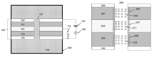
- FIG. 2 a shows the schematic of the charge distribution in the nanofludic field effect transistor at zero gate voltage.
- Charges 201 , 202 , 203 , 204 , 205 correspond to the membrane parts 101 , 102 , 103 , 104 , 105 in FIG. 1 , respectively.
- Charges 206 , 207 , 208 are surface charges on membrane parts 201 , 202 , 203 respectively.
- Charges 206 and 208 are positive charges and 207 are negative charges.
- Charges 208 and 212 are for the case that 103 / 203 is positively charged.
- there is an ionic buffer in the nanochannel 209 there will be counter-ions 210 , 211 , 212 near the charged surface to form an electrical double layer.
- the diameter of the nanochannel 209 is smaller than twice of the thickness of the electrical double layer, the entire nanochannel will be patterned with negative and positive counter-ions (net charge or space charge in the language of semiconductor), forming a structure similar to the MOSFET 213 shown in FIG. 2 b where 214 is a p-type substrate, 215 and 216 are n-doped source and drain areas, 217 is the oxide and 218 is the metal gate.
- the part 103 / 203 can also be uncharged, as shown in FIG. 2 c , although the performance is not that much better than as shown in FIG. 2 a.
- the diameter of the nanochanel 209 can be smaller than 2 nm, but there is no need to be that small.
- the diameter is preferably smaller than twice the Debye length, which could range from 0.3 nm (1 M ionic solution) to 10 nm (0.001 M ionic concentration) depending on the ionic strength of the ionic solution.
- the ionic current between electrodes 204 and 205 through the nanochannel 209 is zero or very small at this zero gate voltage.
- the structure of FIG. 2 a differs from the MOSFET 213 of FIG. 2 b in that the nanofludic field effect transistor is based on controlling the motion of ions through ionic solutions while the MOSFET 213 is based on controlling the motion of electrons or holes through the lattice of solid state materials.
- the ions in the nanofludic FET can also be macro ions or charged biomoleclues, such as DNAs, RNAs, proteins, and so forth, allowing us to control the passage of charged biomolecules through a nanopore/nanochannel.
- FIG. 3 a shows the schematic of the charge distribution in the nanofludic field effect the transistor at a certain gate voltage.
- Films 301 , 302 , 303 , 304 , 305 correspond to the membrane parts 101 , 102 , 103 , 104 , 105 in FIG. 1 respectively.
- Charges 306 , 307 , 308 are surface charges on membrane part 301 , 302 , 303 respectively.
- Charges 306 and 308 are positive charges and 307 are negative charges.
- Inside the nanochannel 309 there are counter-ions 310 , 311 , 312 . Charges 308 and 312 are for the case that the surface of 103 is positively charged.
- FIG. 2 a illustrates that case.
- the associated counter-ions 311 will be redistributed.
- a positive gate voltage will attract more negative ions into the region enclosed by 302 and drive some positive counter-ions 311 out of the region enclosed by 302 .
- This will form a “charge inversion” area 313 , which has no net charge or has net negative ions.
- the area 313 will turn on the ionic current between electrodes 304 and 305 .
- the voltage on gate 302 can change the polarity of the surface charge 307 from negative to positive and accordingly all the counter-ions 311 will be all negative-charged. In this case, it will also turn on the ionic current between electrodes 304 and 305 .
- FIG. 4 shows the schematic of the nanofludic field effect transistor with the three essential parts in the membrane 450 , which is made of layers 401 , 402 and 403 (partitioning the reservoir 406 into two parts).
- source and drain electrodes 404 and 405 are dipped in the ionic buffer 408 .
- a nanometer size hole 407 is made through the membrane 450 by focused electron beam drilling, focused ion beam milling, reactive ion etching or other methods.
- the reservoir 406 and the hole 407 are then filled with an ionic buffer 408 such as water or another solvent.
- Electrodes 404 and 405 are electrodes for measuring ionic current 409 through the hole/nanochannel 407 when a voltage bias 410 is applied on the electrodes.
- the gate voltage 411 applied between membrane parts 402 and 405 can then modulate the ionic current 409 through the hole 407 .
- the principle of turning on the ionic current is the same as shown in FIGS. 2 and 3 . The only difference is that the electrodes 304 and 405 are dipped in the ionic buffer.
- Membrane parts 401 and 403 are made of any electrically insulating material while membrane part 402 is made of any electrically conductive material.
- membrane part 402 one can also put an insulating coating layer on its surface in the nanochannel 407 .
- On the surface that is in contact with the ionic buffer 408 at least one of the membrane parts 401 and 403 has a surface charge of a different polarity than the membrane part 402 .
- Electrodes 404 and 405 could be made of any material for electrochemical electrodes, such as Ag/AgCl; electrodes and Pt electrodes.
- the ionic buffer 408 it can be any ionic solution, such as KCl (potassium chloride) solution, which satisfies the following two conditions: (1) the ionic concentration is low enough that the Debye length is comparable with the diameter of the hole/nanochannel 407 ; and (2) it is at a certain pH value so that the surface charges of at least one of the two films 401 , 403 has different polarity from that of film 402 .
- KCl potassium chloride
- step 510 beginning with an insulating material to form a reservoir, we partition the reservoir with a membrane of at least three layers. One of the layers must be an electrically conductive gate sandwiched between two electrically insulating layers.
- the gate layer must have a surface charge that is different than the surface charge of at least one of the electrically insulating layers.
- the gate could be formed from doped amorphous silicon followed by thermal oxidation of the surface to produce silicon dioxide; while the two layers could be formed of silicon nitride.
- the desired effect in polarizing the layers is to achieve a pH range with a different surface charge polarity in contiguous layers.
- a hole is opened through the membrane.
- This nano-sized hole is a nanochannel or nanopore through which an ionic solution is applied in step 530 .
- the ionic solution can be water or potassium chloride.
- the ionic solution fills the nanochannel and the reservoir.
- the membrane layers of different surface properties transform the nanochannel to a surface-charged modulated ionic channel when interacting with ions such as H + and OH ⁇ , in the solution.
- the surface charge emanates from the interactions between the surface and ions such as H + and OH ⁇ or other similar ions in solution. So different surface properties will generate different surface charge polarities, which are also tunable by the pH of the ionic solution.
- step 540 the source and drain electrodes are introduced and voltage bias is applied between them. These electrodes can be dipped into the ionic solution as shown in FIG. 4 ; or, in the alternative, they can be layered on the membrane as shown in FIG. 1 .
- the source and drain electrodes can be any electrochemical electrodes, such as silver/silver chloride or platinum.
- step 550 we turn on an ionic current by applying voltage to the gate.
- the cause of ionic current is due to the voltage bias applied on source and drain electrodes. Gate voltage simply allows that happen. This allows the transportation of ions through the surface-charge-modulated nanopore/nanochannel. At this point we are able to measure the ionic current through the nanochannel.
- a regular ampmeter can be used to measure the ionic current because it is converted to regular current at the source and drain electrodes. Turning off the voltage halts the movement of the ions through the nanopore/nanochannel.
Landscapes
- Engineering & Computer Science (AREA)
- Health & Medical Sciences (AREA)
- Chemical & Material Sciences (AREA)
- Life Sciences & Earth Sciences (AREA)
- Physics & Mathematics (AREA)
- Biomedical Technology (AREA)
- Nanotechnology (AREA)
- Biochemistry (AREA)
- Molecular Biology (AREA)
- General Health & Medical Sciences (AREA)
- Immunology (AREA)
- Microelectronics & Electronic Packaging (AREA)
- Analytical Chemistry (AREA)
- General Physics & Mathematics (AREA)
- Pathology (AREA)
- Biophysics (AREA)
- Spectroscopy & Molecular Physics (AREA)
- Medicinal Chemistry (AREA)
- Urology & Nephrology (AREA)
- Electrochemistry (AREA)
- Food Science & Technology (AREA)
- Computer Hardware Design (AREA)
- Chemical Kinetics & Catalysis (AREA)
- Hematology (AREA)
- Crystallography & Structural Chemistry (AREA)
- Mathematical Physics (AREA)
- Theoretical Computer Science (AREA)
- Materials Engineering (AREA)
- Investigating Or Analyzing Materials By The Use Of Electric Means (AREA)
- Insulated Gate Type Field-Effect Transistor (AREA)
- Physical Or Chemical Processes And Apparatus (AREA)
Abstract
Description
Claims (18)
Priority Applications (1)
| Application Number | Priority Date | Filing Date | Title |
|---|---|---|---|
| US13/365,577 US8618581B2 (en) | 2009-06-29 | 2012-02-03 | Nanofludic field effect transistor based on surface charge modulated nanochannel |
Applications Claiming Priority (2)
| Application Number | Priority Date | Filing Date | Title |
|---|---|---|---|
| US12/493,811 US8110410B2 (en) | 2009-06-29 | 2009-06-29 | Nanofludic field effect transistor based on surface charge modulated nanochannel |
| US13/365,577 US8618581B2 (en) | 2009-06-29 | 2012-02-03 | Nanofludic field effect transistor based on surface charge modulated nanochannel |
Related Parent Applications (1)
| Application Number | Title | Priority Date | Filing Date |
|---|---|---|---|
| US12/493,811 Division US8110410B2 (en) | 2009-06-29 | 2009-06-29 | Nanofludic field effect transistor based on surface charge modulated nanochannel |
Publications (2)
| Publication Number | Publication Date |
|---|---|
| US20120132886A1 US20120132886A1 (en) | 2012-05-31 |
| US8618581B2 true US8618581B2 (en) | 2013-12-31 |
Family
ID=43379694
Family Applications (2)
| Application Number | Title | Priority Date | Filing Date |
|---|---|---|---|
| US12/493,811 Expired - Fee Related US8110410B2 (en) | 2009-06-29 | 2009-06-29 | Nanofludic field effect transistor based on surface charge modulated nanochannel |
| US13/365,577 Active 2029-09-04 US8618581B2 (en) | 2009-06-29 | 2012-02-03 | Nanofludic field effect transistor based on surface charge modulated nanochannel |
Family Applications Before (1)
| Application Number | Title | Priority Date | Filing Date |
|---|---|---|---|
| US12/493,811 Expired - Fee Related US8110410B2 (en) | 2009-06-29 | 2009-06-29 | Nanofludic field effect transistor based on surface charge modulated nanochannel |
Country Status (3)
| Country | Link |
|---|---|
| US (2) | US8110410B2 (en) |
| JP (1) | JP5443282B2 (en) |
| KR (1) | KR101581051B1 (en) |
Cited By (1)
| Publication number | Priority date | Publication date | Assignee | Title |
|---|---|---|---|---|
| US9945836B2 (en) | 2015-04-23 | 2018-04-17 | International Business Machines Corporation | Field effect based nanopore device |
Families Citing this family (42)
| Publication number | Priority date | Publication date | Assignee | Title |
|---|---|---|---|---|
| US9632073B2 (en) | 2012-04-02 | 2017-04-25 | Lux Bio Group, Inc. | Apparatus and method for molecular separation, purification, and sensing |
| US7638034B2 (en) | 2006-09-21 | 2009-12-29 | Los Alamos National Security, Llc | Electrochemical detection of single molecules using abiotic nanopores having electrically tunable dimensions |
| US8084319B2 (en) * | 2010-02-12 | 2011-12-27 | International Business Machines Corporation | Precisely tuning feature sizes on hard masks via plasma treatment |
| US9194838B2 (en) | 2010-03-03 | 2015-11-24 | Osaka University | Method and device for identifying nucleotide, and method and device for determining nucleotide sequence of polynucleotide |
| US8603303B2 (en) * | 2010-03-15 | 2013-12-10 | International Business Machines Corporation | Nanopore based device for cutting long DNA molecules into fragments |
| US8039250B2 (en) * | 2010-03-15 | 2011-10-18 | International Business Machines Corporation | Piezoelectric-based nanopore device for the active control of the motion of polymers through the same |
| US8828138B2 (en) | 2010-05-17 | 2014-09-09 | International Business Machines Corporation | FET nanopore sensor |
| US8986524B2 (en) | 2011-01-28 | 2015-03-24 | International Business Machines Corporation | DNA sequence using multiple metal layer structure with different organic coatings forming different transient bondings to DNA |
| US20120193231A1 (en) | 2011-01-28 | 2012-08-02 | International Business Machines Corporation | Dna sequencing using multiple metal layer structure with organic coatings forming transient bonding to dna bases |
| US8852407B2 (en) | 2011-01-28 | 2014-10-07 | International Business Machines Corporation | Electron beam sculpting of tunneling junction for nanopore DNA sequencing |
| US8518829B2 (en) * | 2011-04-22 | 2013-08-27 | International Business Machines Corporation | Self-sealed fluidic channels for nanopore array |
| CN104011866B (en) * | 2011-07-27 | 2017-06-09 | 伊利诺伊大学评议会 | For the nanopore sensor that biomolecule is characterized |
| KR101922127B1 (en) * | 2012-03-13 | 2018-11-26 | 삼성전자주식회사 | Nanopore device with improved sensitivity and method of fabricating the same |
| US9732384B2 (en) | 2012-04-02 | 2017-08-15 | Lux Bio Group, Inc. | Apparatus and method for molecular separation, purification, and sensing |
| CN109061128A (en) * | 2012-04-02 | 2018-12-21 | 力士生物集团公司 | Device and method for molecule separation, purifying and detection |
| US10029915B2 (en) | 2012-04-04 | 2018-07-24 | International Business Machines Corporation | Functionally switchable self-assembled coating compound for controlling translocation of molecule through nanopores |
| CN104769424B (en) | 2012-04-09 | 2017-11-10 | 巴拉什·塔库拉帕里 | Field-effect transistor, the device comprising the transistor and its formation and application method |
| US8737114B2 (en) | 2012-05-07 | 2014-05-27 | Micron Technology, Inc. | Switching device structures and methods |
| WO2014027580A1 (en) | 2012-08-17 | 2014-02-20 | 国立大学法人大阪大学 | Sample analysis method |
| US10526218B2 (en) * | 2012-10-01 | 2020-01-07 | The Board Of Trustees Of The Leland Stanford Junior University | Flow control method and apparatuses |
| US8906215B2 (en) * | 2012-11-30 | 2014-12-09 | International Business Machines Corporation | Field effect based nanosensor for biopolymer manipulation and detection |
| JP6282036B2 (en) | 2012-12-27 | 2018-02-21 | クオンタムバイオシステムズ株式会社 | Method and control apparatus for controlling movement speed of substance |
| KR101419742B1 (en) * | 2013-02-19 | 2014-07-21 | 연세대학교 산학협력단 | Highly efficient nanofluidic energy harvesting system and method using ionic field-effect transistor |
| US9322820B2 (en) * | 2013-03-14 | 2016-04-26 | Wisconsin Alumni Research Foundation | System and apparatus for nanopore sequencing |
| US9046511B2 (en) | 2013-04-18 | 2015-06-02 | International Business Machines Corporation | Fabrication of tunneling junction for nanopore DNA sequencing |
| US9182369B2 (en) | 2013-06-19 | 2015-11-10 | Globalfoundries Inc. | Manufacturable sub-3 nanometer palladium gap devices for fixed electrode tunneling recognition |
| US9188578B2 (en) | 2013-06-19 | 2015-11-17 | Globalfoundries Inc. | Nanogap device with capped nanowire structures |
| JP5966086B2 (en) | 2013-06-28 | 2016-08-10 | 株式会社日立ハイテクノロジーズ | Analysis equipment |
| US10058821B2 (en) * | 2013-09-13 | 2018-08-28 | Infineon Technologies Ag | Ion pump |
| CA2929929A1 (en) | 2013-09-18 | 2015-03-26 | Quantum Biosystems Inc. | Biomolecule sequencing devices, systems and methods |
| JP2015077652A (en) | 2013-10-16 | 2015-04-23 | クオンタムバイオシステムズ株式会社 | Nano-gap electrode and method for manufacturing same |
| US10438811B1 (en) | 2014-04-15 | 2019-10-08 | Quantum Biosystems Inc. | Methods for forming nano-gap electrodes for use in nanosensors |
| US10967372B2 (en) * | 2014-04-16 | 2021-04-06 | International Business Machines Corporation | Electro-fluidic flow probe |
| US10030265B2 (en) * | 2015-01-14 | 2018-07-24 | International Business Machines Corporation | DNA sequencing using MOSFET transistors |
| CN107530638B (en) * | 2015-02-24 | 2021-03-09 | 渥太华大学 | Positioning nanopore fabrication on membrane by laser irradiation during controlled breakdown |
| KR101597936B1 (en) * | 2015-04-16 | 2016-02-25 | 고려대학교 산학협력단 | Ion channel device |
| KR101868221B1 (en) * | 2016-03-14 | 2018-06-15 | 고려대학교 산학협력단 | Ion Channel Pressure Sensor And The Manufacturing Method Of The Same |
| US10429343B1 (en) | 2017-02-09 | 2019-10-01 | National Technology & Engineering Solutions Of Sandia, Llc | Tunable ionic electronic transistor |
| US11131646B2 (en) * | 2017-11-03 | 2021-09-28 | Robert Bosch Gmbh | Electrochemical sequencing of DNA using an edge electrode |
| WO2021146537A1 (en) * | 2020-01-15 | 2021-07-22 | The Methodist Hospital System | Electrostatically gated nanofluidic membranes for control of molecular transport |
| US11913971B2 (en) | 2021-02-24 | 2024-02-27 | Globalfoundries U.S. Inc. | Motion-sensitive field effect transistor, motion detection system, and method |
| CN113311048B (en) * | 2021-05-25 | 2024-03-12 | 南通大学 | Nanofluidic field effect transistor and preparation method and application thereof |
Citations (2)
| Publication number | Priority date | Publication date | Assignee | Title |
|---|---|---|---|---|
| US20040007740A1 (en) * | 2002-05-15 | 2004-01-15 | Gerhard Abstreiter | Silicon-on-insulator biosensor device |
| US20110139637A1 (en) * | 2008-08-08 | 2011-06-16 | Electronics And Telecommunications Research Institute | Method and apparatus for measuring isoelectric point using field effect transistor |
Family Cites Families (7)
| Publication number | Priority date | Publication date | Assignee | Title |
|---|---|---|---|---|
| JPH0625745B2 (en) * | 1985-09-30 | 1994-04-06 | 株式会社東芝 | Semiconductor sensor |
| JP2002228628A (en) * | 2001-01-31 | 2002-08-14 | Horiba Ltd | Device for measuring ion concentration |
| DE60228685D1 (en) | 2002-05-16 | 2008-10-16 | Micronit Microfluidics Bv | Method for producing a microfluidic component |
| US20070286773A1 (en) | 2002-05-16 | 2007-12-13 | Micronit Microfluidics B.V. | Microfluidic Device |
| US20060086626A1 (en) * | 2004-10-22 | 2006-04-27 | Joyce Timothy H | Nanostructure resonant tunneling with a gate voltage source |
| US7918244B2 (en) | 2005-05-02 | 2011-04-05 | Massachusetts Institute Of Technology | Microfluidic bubble logic devices |
| KR100773549B1 (en) * | 2006-04-03 | 2007-11-07 | 삼성전자주식회사 | Method of detecting bio-molecules using the same field effect transistor |
-
2009
- 2009-06-29 US US12/493,811 patent/US8110410B2/en not_active Expired - Fee Related
-
2010
- 2010-06-21 KR KR1020100058330A patent/KR101581051B1/en not_active IP Right Cessation
- 2010-06-24 JP JP2010143601A patent/JP5443282B2/en not_active Expired - Fee Related
-
2012
- 2012-02-03 US US13/365,577 patent/US8618581B2/en active Active
Patent Citations (2)
| Publication number | Priority date | Publication date | Assignee | Title |
|---|---|---|---|---|
| US20040007740A1 (en) * | 2002-05-15 | 2004-01-15 | Gerhard Abstreiter | Silicon-on-insulator biosensor device |
| US20110139637A1 (en) * | 2008-08-08 | 2011-06-16 | Electronics And Telecommunications Research Institute | Method and apparatus for measuring isoelectric point using field effect transistor |
Cited By (2)
| Publication number | Priority date | Publication date | Assignee | Title |
|---|---|---|---|---|
| US9945836B2 (en) | 2015-04-23 | 2018-04-17 | International Business Machines Corporation | Field effect based nanopore device |
| US10261067B2 (en) | 2015-04-23 | 2019-04-16 | International Business Machines Corporation | Method of forming a field effect based nanopore device |
Also Published As
| Publication number | Publication date |
|---|---|
| US20100327255A1 (en) | 2010-12-30 |
| JP2011007793A (en) | 2011-01-13 |
| JP5443282B2 (en) | 2014-03-19 |
| KR101581051B1 (en) | 2016-01-11 |
| US8110410B2 (en) | 2012-02-07 |
| KR20110001896A (en) | 2011-01-06 |
| US20120132886A1 (en) | 2012-05-31 |
Similar Documents
| Publication | Publication Date | Title |
|---|---|---|
| US8618581B2 (en) | Nanofludic field effect transistor based on surface charge modulated nanochannel | |
| Jiang et al. | 2D MoS2 neuromorphic devices for brain‐like computational systems | |
| Zhang et al. | Tunable charge-trap memory based on few-layer MoS2 | |
| Chakraborty et al. | Analytical modeling and sensitivity analysis of dielectric-modulated junctionless gate stack surrounding gate MOSFET (JLGSSRG) for application as biosensor | |
| Xiao et al. | Room-temperature-processed flexible amorphous InGaZnO thin film transistor | |
| Mabeck et al. | Microfluidic gating of an organic electrochemical transistor | |
| Park et al. | Nonvolatile and neuromorphic memory devices using interfacial traps in two-dimensional WSe2/MoTe2 stack channel | |
| Joshi et al. | Field effect modulation of ionic conductance of cylindrical silicon-on-insulator nanopore array | |
| Zhou et al. | Gated ion transport in a soft nanochannel with biomimetic polyelectrolyte brush layers | |
| Sonmez et al. | Modelling and realization of a water-gated field effect transistor (WG-FET) using 16-nm-thick mono-Si film | |
| Chiu et al. | Graphene memory based on a tunable nanometer-thin water layer | |
| JP2019504501A (en) | Structure for improving switching speed of transistor using polar elastomer | |
| US20120298531A1 (en) | Dual FET Sensor for Sensing Biomolecules & Charged Ions in an Electrolyte | |
| Chen et al. | Polarized Tunneling Transistor for Ultrafast Memory | |
| Xie et al. | Copper atomic-scale transistors | |
| CN206789549U (en) | A kind of two-dimensional semiconductor negative capacitance FET | |
| Selvarajan et al. | Transfer characteristics of graphene based field effect transistor (GFET) for biosensing application | |
| Ertop et al. | Realization of a planar water-gated field effect transistor (WG-FET) using 16-nm-thick single crystalline Si film | |
| Jeon et al. | Tuning the on/off current ratio in ionic-liquid gated multi-layer MoS2 field-effect transistors | |
| Naorem et al. | Ionic liquid channel field effect transistor fabricated using silicon dioxide trench | |
| Maurya et al. | Fluid-FET: an ionic controller for lab-on-a-chip | |
| Kuznetsov et al. | Study of the sensitivity of pH-sensors based on silicon MOS-nanotransistors | |
| Singh et al. | Comparative Analysis of Underlapped Silicon on Insulator and Underlapped Silicon on Nothing Dielectric and Charge Modulated FET based Biosensors | |
| KR102118608B1 (en) | Switching element based on vertical structures utilizing 2-dimensional nano-materials and dielectric-double layer | |
| Kim et al. | Modeling of a Stacked Gated Nanofluidic Channel |
Legal Events
| Date | Code | Title | Description |
|---|---|---|---|
| STCF | Information on status: patent grant |
Free format text: PATENTED CASE |
|
| AS | Assignment |
Owner name: GLOBALFOUNDRIES U.S. 2 LLC, NEW YORK Free format text: ASSIGNMENT OF ASSIGNORS INTEREST;ASSIGNOR:INTERNATIONAL BUSINESS MACHINES CORPORATION;REEL/FRAME:036550/0001 Effective date: 20150629 |
|
| AS | Assignment |
Owner name: GLOBALFOUNDRIES INC., CAYMAN ISLANDS Free format text: ASSIGNMENT OF ASSIGNORS INTEREST;ASSIGNORS:GLOBALFOUNDRIES U.S. 2 LLC;GLOBALFOUNDRIES U.S. INC.;REEL/FRAME:036779/0001 Effective date: 20150910 |
|
| FPAY | Fee payment |
Year of fee payment: 4 |
|
| AS | Assignment |
Owner name: WILMINGTON TRUST, NATIONAL ASSOCIATION, DELAWARE Free format text: SECURITY AGREEMENT;ASSIGNOR:GLOBALFOUNDRIES INC.;REEL/FRAME:049490/0001 Effective date: 20181127 |
|
| AS | Assignment |
Owner name: GLOBALFOUNDRIES INC., CAYMAN ISLANDS Free format text: RELEASE BY SECURED PARTY;ASSIGNOR:WILMINGTON TRUST, NATIONAL ASSOCIATION;REEL/FRAME:054479/0842 Effective date: 20200410 Owner name: TAIWAN SEMICONDUCTOR MANUFACTURING CO., LTD., TAIWAN Free format text: ASSIGNMENT OF ASSIGNORS INTEREST;ASSIGNOR:GLOBALFOUNDRIES INC.;REEL/FRAME:054482/0862 Effective date: 20200515 |
|
| AS | Assignment |
Owner name: GLOBALFOUNDRIES INC., CAYMAN ISLANDS Free format text: RELEASE BY SECURED PARTY;ASSIGNOR:WILMINGTON TRUST, NATIONAL ASSOCIATION;REEL/FRAME:054636/0001 Effective date: 20201117 |
|
| FEPP | Fee payment procedure |
Free format text: MAINTENANCE FEE REMINDER MAILED (ORIGINAL EVENT CODE: REM.); ENTITY STATUS OF PATENT OWNER: LARGE ENTITY |
|
| FEPP | Fee payment procedure |
Free format text: 7.5 YR SURCHARGE - LATE PMT W/IN 6 MO, LARGE ENTITY (ORIGINAL EVENT CODE: M1555); ENTITY STATUS OF PATENT OWNER: LARGE ENTITY |
|
| MAFP | Maintenance fee payment |
Free format text: PAYMENT OF MAINTENANCE FEE, 8TH YEAR, LARGE ENTITY (ORIGINAL EVENT CODE: M1552); ENTITY STATUS OF PATENT OWNER: LARGE ENTITY Year of fee payment: 8 |