US8615028B1 - Vertically integrated optical phased array with pseudo-random array architecture - Google Patents
Vertically integrated optical phased array with pseudo-random array architecture Download PDFInfo
- Publication number
- US8615028B1 US8615028B1 US12/902,657 US90265710A US8615028B1 US 8615028 B1 US8615028 B1 US 8615028B1 US 90265710 A US90265710 A US 90265710A US 8615028 B1 US8615028 B1 US 8615028B1
- Authority
- US
- United States
- Prior art keywords
- vertical cavity
- array
- surface emitting
- disposed
- emitting lasers
- Prior art date
- Legal status (The legal status is an assumption and is not a legal conclusion. Google has not performed a legal analysis and makes no representation as to the accuracy of the status listed.)
- Expired - Fee Related, expires
Links
Images


Classifications
-
- H—ELECTRICITY
- H01—ELECTRIC ELEMENTS
- H01S—DEVICES USING THE PROCESS OF LIGHT AMPLIFICATION BY STIMULATED EMISSION OF RADIATION [LASER] TO AMPLIFY OR GENERATE LIGHT; DEVICES USING STIMULATED EMISSION OF ELECTROMAGNETIC RADIATION IN WAVE RANGES OTHER THAN OPTICAL
- H01S5/00—Semiconductor lasers
- H01S5/40—Arrangement of two or more semiconductor lasers, not provided for in groups H01S5/02 - H01S5/30
- H01S5/4006—Injection locking
-
- H—ELECTRICITY
- H01—ELECTRIC ELEMENTS
- H01S—DEVICES USING THE PROCESS OF LIGHT AMPLIFICATION BY STIMULATED EMISSION OF RADIATION [LASER] TO AMPLIFY OR GENERATE LIGHT; DEVICES USING STIMULATED EMISSION OF ELECTROMAGNETIC RADIATION IN WAVE RANGES OTHER THAN OPTICAL
- H01S5/00—Semiconductor lasers
- H01S5/40—Arrangement of two or more semiconductor lasers, not provided for in groups H01S5/02 - H01S5/30
- H01S5/42—Arrays of surface emitting lasers
- H01S5/423—Arrays of surface emitting lasers having a vertical cavity
-
- H—ELECTRICITY
- H01—ELECTRIC ELEMENTS
- H01S—DEVICES USING THE PROCESS OF LIGHT AMPLIFICATION BY STIMULATED EMISSION OF RADIATION [LASER] TO AMPLIFY OR GENERATE LIGHT; DEVICES USING STIMULATED EMISSION OF ELECTROMAGNETIC RADIATION IN WAVE RANGES OTHER THAN OPTICAL
- H01S2301/00—Functional characteristics
- H01S2301/20—Lasers with a special output beam profile or cross-section, e.g. non-Gaussian
-
- H—ELECTRICITY
- H01—ELECTRIC ELEMENTS
- H01S—DEVICES USING THE PROCESS OF LIGHT AMPLIFICATION BY STIMULATED EMISSION OF RADIATION [LASER] TO AMPLIFY OR GENERATE LIGHT; DEVICES USING STIMULATED EMISSION OF ELECTROMAGNETIC RADIATION IN WAVE RANGES OTHER THAN OPTICAL
- H01S5/00—Semiconductor lasers
- H01S5/005—Optical components external to the laser cavity, specially adapted therefor, e.g. for homogenisation or merging of the beams or for manipulating laser pulses, e.g. pulse shaping
- H01S5/0085—Optical components external to the laser cavity, specially adapted therefor, e.g. for homogenisation or merging of the beams or for manipulating laser pulses, e.g. pulse shaping for modulating the output, i.e. the laser beam is modulated outside the laser cavity
-
- H—ELECTRICITY
- H01—ELECTRIC ELEMENTS
- H01S—DEVICES USING THE PROCESS OF LIGHT AMPLIFICATION BY STIMULATED EMISSION OF RADIATION [LASER] TO AMPLIFY OR GENERATE LIGHT; DEVICES USING STIMULATED EMISSION OF ELECTROMAGNETIC RADIATION IN WAVE RANGES OTHER THAN OPTICAL
- H01S5/00—Semiconductor lasers
- H01S5/02—Structural details or components not essential to laser action
- H01S5/026—Monolithically integrated components, e.g. waveguides, monitoring photo-detectors, drivers
-
- H—ELECTRICITY
- H01—ELECTRIC ELEMENTS
- H01S—DEVICES USING THE PROCESS OF LIGHT AMPLIFICATION BY STIMULATED EMISSION OF RADIATION [LASER] TO AMPLIFY OR GENERATE LIGHT; DEVICES USING STIMULATED EMISSION OF ELECTROMAGNETIC RADIATION IN WAVE RANGES OTHER THAN OPTICAL
- H01S5/00—Semiconductor lasers
- H01S5/06—Arrangements for controlling the laser output parameters, e.g. by operating on the active medium
- H01S5/062—Arrangements for controlling the laser output parameters, e.g. by operating on the active medium by varying the potential of the electrodes
- H01S5/06233—Controlling other output parameters than intensity or frequency
- H01S5/06246—Controlling other output parameters than intensity or frequency controlling the phase
-
- H—ELECTRICITY
- H01—ELECTRIC ELEMENTS
- H01S—DEVICES USING THE PROCESS OF LIGHT AMPLIFICATION BY STIMULATED EMISSION OF RADIATION [LASER] TO AMPLIFY OR GENERATE LIGHT; DEVICES USING STIMULATED EMISSION OF ELECTROMAGNETIC RADIATION IN WAVE RANGES OTHER THAN OPTICAL
- H01S5/00—Semiconductor lasers
- H01S5/10—Construction or shape of the optical resonator, e.g. extended or external cavity, coupled cavities, bent-guide, varying width, thickness or composition of the active region
- H01S5/18—Surface-emitting [SE] lasers, e.g. having both horizontal and vertical cavities
- H01S5/183—Surface-emitting [SE] lasers, e.g. having both horizontal and vertical cavities having only vertical cavities, e.g. vertical cavity surface-emitting lasers [VCSEL]
- H01S5/18302—Surface-emitting [SE] lasers, e.g. having both horizontal and vertical cavities having only vertical cavities, e.g. vertical cavity surface-emitting lasers [VCSEL] comprising an integrated optical modulator
Definitions
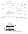
- a master laser 12 and a preferably 2-D array of gratings 16 that provide ports for out-coupling the laser radiation of the master laser 12 in a vertical direction, forming the 2-D array of coherent beamlets 18 which, in use, injection lock the lasers of the VCSELs 10 .
- the master laser 12 is preferably a DBR laser and the ports may be implemented by gratings 16 , all of which may be disposed on or in an outcoupler substrate 100 shown, for example, in FIG. 2 k which is described in greater detail below.
- the gratings 16 in the substrate 100 optically align with the lasers of the VCSEL array 10 and therefore are disposed in the same aperiodic or randomized pattern as selected for the array of VCSELs 10 .
- Laser beamlets 18 are emitted from outcoupler substrate 110 as an array of beamlets 18 (with the same predetermined aperiodic or randomized pattern mentioned above) in a vertical direction towards the array of VCMODs 20 which impose a variable phase change to each beamlet.
- the amount of phase change at each VCMOD 20 is initially calibrated using an external fiber-based interferometric measurement system.
- Each beamlet 18 then exits its associated VCMOD 20 in substrate 120 and enters a corresponding VCSEL 10 to injection lock it.
- the VCSELs 10 emit a corresponding beam 5 which form an array of beams (with the same predetermined aperiodic or randomized pattern mentioned above), again in a vertical direction, towards the phase control substrate 130 .
- the grating couplers 25 in the phase control substrate 130 are arranged in the same predetermined aperiodic or randomized pattern mentioned above to sample a corresponding portion of the light emitted as beams 5 as will be discussed in greater detail below.
- the beams 5 exit the phase control substrate 130 and as a steered beam exiting an optical phased array.
Landscapes
- Physics & Mathematics (AREA)
- Condensed Matter Physics & Semiconductors (AREA)
- General Physics & Mathematics (AREA)
- Electromagnetism (AREA)
- Optics & Photonics (AREA)
- Semiconductor Lasers (AREA)
Abstract
Description
| Waveguide | ||||
| Self-Locked | OPA | |||
| OPA Technology | V-OPA | VCSELs | LC-OPA | |
| OPA Dimension | ||||
| 2 | 2 | 2 | 1 | |
| Beam Scanning | <1 ns | <1 ns | >10 ms | <1 ns |
| Speed | ||||
| Phase shift per | 2π | <π/2 | <2π | 2π |
| element | (cm long WG) | |||
| Grating Lobes | No | Yes | Yes | Yes |
| Mode hopping | No | Yes | N/A | No |
| Indep. phase/amp | Yes | No | No | Yes |
| control | ||||
where, Δφr is the single-pass roundtrip phase shift in the cavity with finesse F, Δn is the carrier-induced index change in the MQW, LC is the F-P cavity length, and R is the effective reflectivity of the cavity mirrors. For Δn=5×10⁻³, LC=˜1 μm, a cavity finesse of about 100 is required for an effective phase change of ΔφM=2π. This finesse value can be achieved with cavity mirror reflectivities of about 97%. The minimum optical transmission of the above VCMOD structure is about 0.2 obtained at a maximum phase change of 2π. Variations in the intensity of the injection signal by a factor of 5 results in a change of a factor of about 2.2 in the frequency locking range of the slave lasers. For example, for a typical optical injection ratio of 2×10⁻⁴ at maximum VCMOD transmission, the VCSEL locking bandwidth is calculated to decrease from 7.4 GHz to 3.4 GHz when the optical phase is modulated from 0 to 2π. Stable injection locking can be achieved within this range of locking bandwidth, for example by using a 600 mW master laser to feed 8000 emitting elements in the V-OPA.
Claims (28)
Priority Applications (1)
| Application Number | Priority Date | Filing Date | Title |
|---|---|---|---|
| US12/902,657 US8615028B1 (en) | 2010-10-12 | 2010-10-12 | Vertically integrated optical phased array with pseudo-random array architecture |
Applications Claiming Priority (1)
| Application Number | Priority Date | Filing Date | Title |
|---|---|---|---|
| US12/902,657 US8615028B1 (en) | 2010-10-12 | 2010-10-12 | Vertically integrated optical phased array with pseudo-random array architecture |
Publications (1)
| Publication Number | Publication Date |
|---|---|
| US8615028B1 true US8615028B1 (en) | 2013-12-24 |
Family
ID=49770106
Family Applications (1)
| Application Number | Title | Priority Date | Filing Date |
|---|---|---|---|
| US12/902,657 Expired - Fee Related US8615028B1 (en) | 2010-10-12 | 2010-10-12 | Vertically integrated optical phased array with pseudo-random array architecture |
Country Status (1)
| Country | Link |
|---|---|
| US (1) | US8615028B1 (en) |
Cited By (18)
| Publication number | Priority date | Publication date | Assignee | Title |
|---|---|---|---|---|
| US20120293625A1 (en) * | 2011-05-18 | 2012-11-22 | Sick Ag | 3d-camera and method for the three-dimensional monitoring of a monitoring area |
| CN107994459A (en) * | 2017-12-30 | 2018-05-04 | 北京工业大学 | Export the laser array of coherent laser |
| EP3259812A4 (en) * | 2015-02-20 | 2018-11-14 | HRL Laboratories, LLC | Chip-scale power scalable ultraviolet optical source |
| US20190064332A1 (en) * | 2017-08-24 | 2019-02-28 | Toyota Motor Engineering & Manufacturing North America, Inc. | Photonics integrated phase measurement |
| US10345518B1 (en) | 2013-05-30 | 2019-07-09 | Hrl Laboratories, Llc | Multi-wavelength band optical phase and amplitude controller |
| US10408673B2 (en) * | 2014-06-09 | 2019-09-10 | Stc.Unm | Integrated bound-mode spectral/angular sensors |
| US10481328B1 (en) * | 2018-10-16 | 2019-11-19 | Honeywell International Inc. | Optical phased array with integrated secondary optics |
| DE102018123320A1 (en) * | 2018-09-21 | 2020-03-26 | Osram Opto Semiconductors Gmbh | Phase-coupled laser arrangement and method for producing a phase-coupled laser arrangement |
| US10613410B2 (en) | 2016-10-14 | 2020-04-07 | Analog Photonics LLC | Large scale optical phased array |
| US11073737B2 (en) * | 2018-12-31 | 2021-07-27 | Luxtera Llc | Method and system for an all-optical wafer acceptance test |
| US11402670B2 (en) | 2019-09-23 | 2022-08-02 | Samsung Electronics Co., Ltd. | Light modulator, beam steering device including the light modulator, and electronic device including the beam steering device |
| US11480463B2 (en) | 2014-06-09 | 2022-10-25 | Unm Rainforest Innovations | Integrated bound-mode spectral/angular sensors |
| CN115275777A (en) * | 2022-06-22 | 2022-11-01 | 北京工业大学 | Two-phase array VCSEL laser beam control device and preparation method |
| WO2024017891A1 (en) * | 2022-07-19 | 2024-01-25 | Powerphotonic Ltd | Coherent beam combination method and apparatus |
| WO2024124502A1 (en) * | 2022-12-15 | 2024-06-20 | 华为技术有限公司 | Optical phased array assembly, laser emission system, laser radar, and vehicle |
| US12301289B1 (en) | 2021-01-24 | 2025-05-13 | Cable Television Laboratories, Inc. | Systems and methods for free space optical injection locking |
| US12322928B2 (en) | 2021-09-03 | 2025-06-03 | Eagle Technology, Llc | Optical device including laterally guided vertical-cavity surface-emitting lasers (VCSELs) outputs and related methods |
| US12368277B1 (en) * | 2021-01-24 | 2025-07-22 | Cable Television Laboratories, Inc. | Systems and methods for free space optical injection locking |
Citations (5)
| Publication number | Priority date | Publication date | Assignee | Title |
|---|---|---|---|---|
| US4649351A (en) * | 1984-10-19 | 1987-03-10 | Massachusetts Institute Of Technology | Apparatus and method for coherently adding laser beams |
| US5568574A (en) * | 1995-06-12 | 1996-10-22 | University Of Southern California | Modulator-based photonic chip-to-chip interconnections for dense three-dimensional multichip module integration |
| US20030103534A1 (en) * | 2001-11-30 | 2003-06-05 | Braiman Yehuda Y. | Master laser injection of board area lasers |
| US20040066808A1 (en) * | 2001-06-29 | 2004-04-08 | John Trezza | Integrated arrays of modulators and lasers on electronics |
| US20110052114A1 (en) * | 2009-09-02 | 2011-03-03 | Alcatel-Lucent Usa Inc. | Vertical optically emitting photonic devices with electronic steering capability |
-
2010
- 2010-10-12 US US12/902,657 patent/US8615028B1/en not_active Expired - Fee Related
Patent Citations (5)
| Publication number | Priority date | Publication date | Assignee | Title |
|---|---|---|---|---|
| US4649351A (en) * | 1984-10-19 | 1987-03-10 | Massachusetts Institute Of Technology | Apparatus and method for coherently adding laser beams |
| US5568574A (en) * | 1995-06-12 | 1996-10-22 | University Of Southern California | Modulator-based photonic chip-to-chip interconnections for dense three-dimensional multichip module integration |
| US20040066808A1 (en) * | 2001-06-29 | 2004-04-08 | John Trezza | Integrated arrays of modulators and lasers on electronics |
| US20030103534A1 (en) * | 2001-11-30 | 2003-06-05 | Braiman Yehuda Y. | Master laser injection of board area lasers |
| US20110052114A1 (en) * | 2009-09-02 | 2011-03-03 | Alcatel-Lucent Usa Inc. | Vertical optically emitting photonic devices with electronic steering capability |
Non-Patent Citations (5)
| Title |
|---|
| A.C. Lehman et. al., Applied Physics Letters, vol. 88 (2006) p. 021102. |
| F. Vasey et. al., Applied Optics, vol. 32 (1993) p. 3220. |
| Jean-Francois Seurin et. al., Proc. Of SPIE, vol. 6908 (2008). |
| P.F. McManamon et. al., Proceedings of IEEE, vol. 84, No. 2 (1996) p. 268. |
| R.H. Yan et. al., IEEE J. Quant. Electron., vol. 25, No. 11(1989). |
Cited By (31)
| Publication number | Priority date | Publication date | Assignee | Title |
|---|---|---|---|---|
| US9228697B2 (en) * | 2011-05-18 | 2016-01-05 | Sick Ag | 3D-camera and method for the three-dimensional monitoring of a monitoring area |
| US20120293625A1 (en) * | 2011-05-18 | 2012-11-22 | Sick Ag | 3d-camera and method for the three-dimensional monitoring of a monitoring area |
| US10345518B1 (en) | 2013-05-30 | 2019-07-09 | Hrl Laboratories, Llc | Multi-wavelength band optical phase and amplitude controller |
| US10613411B1 (en) * | 2013-05-30 | 2020-04-07 | Hrl Laboratories, Llc | Pseudo-randomly spaced two-dimensional phased array assembly |
| US10989590B2 (en) * | 2014-06-09 | 2021-04-27 | Unm Rainforest Innovations | Integrated bound-mode spectral/angular sensors |
| US10408673B2 (en) * | 2014-06-09 | 2019-09-10 | Stc.Unm | Integrated bound-mode spectral/angular sensors |
| US12460967B2 (en) | 2014-06-09 | 2025-11-04 | Unm Rainforest Innovations | Integrated bound-mode spectral/angular sensors |
| US11480463B2 (en) | 2014-06-09 | 2022-10-25 | Unm Rainforest Innovations | Integrated bound-mode spectral/angular sensors |
| EP3259812A4 (en) * | 2015-02-20 | 2018-11-14 | HRL Laboratories, LLC | Chip-scale power scalable ultraviolet optical source |
| US10613410B2 (en) | 2016-10-14 | 2020-04-07 | Analog Photonics LLC | Large scale optical phased array |
| US20190064332A1 (en) * | 2017-08-24 | 2019-02-28 | Toyota Motor Engineering & Manufacturing North America, Inc. | Photonics integrated phase measurement |
| US10627496B2 (en) * | 2017-08-24 | 2020-04-21 | Toyota Motor Engineering & Manufacturing North America, Inc. | Photonics integrated phase measurement |
| CN107994459A (en) * | 2017-12-30 | 2018-05-04 | 北京工业大学 | Export the laser array of coherent laser |
| CN107994459B (en) * | 2017-12-30 | 2019-08-16 | 北京工业大学 | Laser array that outputs coherent laser light |
| JP2022500880A (en) * | 2018-09-21 | 2022-01-04 | オスラム オーエルイーディー ゲゼルシャフト ミット ベシュレンクテル ハフツングOSRAM OLED GmbH | Phase-coupled laser devices and methods for manufacturing phase-coupled laser devices. |
| US20210273400A1 (en) * | 2018-09-21 | 2021-09-02 | Osram Oled Gmbh | Phase-coupled laser assembly and method for producing a phase-coupled laser assembly |
| WO2020057856A1 (en) * | 2018-09-21 | 2020-03-26 | Osram Oled Gmbh | Phase-coupled laser assembly and method for producing a phase-coupled laser assembly |
| DE102018123320A1 (en) * | 2018-09-21 | 2020-03-26 | Osram Opto Semiconductors Gmbh | Phase-coupled laser arrangement and method for producing a phase-coupled laser arrangement |
| DE102018123320B4 (en) | 2018-09-21 | 2023-01-26 | OSRAM Opto Semiconductors Gesellschaft mit beschränkter Haftung | Phase-locked laser assembly and method of manufacturing a phase-locked laser assembly |
| JP7293348B2 (en) | 2018-09-21 | 2023-06-19 | オスラム オーエルイーディー ゲゼルシャフト ミット ベシュレンクテル ハフツング | Phase-coupled laser device and method for manufacturing a phase-coupled laser device |
| US11923656B2 (en) * | 2018-09-21 | 2024-03-05 | Osram Oled Gmbh | Phase-coupled laser assembly and method for producing a phase-coupled laser assembly |
| US10481328B1 (en) * | 2018-10-16 | 2019-11-19 | Honeywell International Inc. | Optical phased array with integrated secondary optics |
| US11073737B2 (en) * | 2018-12-31 | 2021-07-27 | Luxtera Llc | Method and system for an all-optical wafer acceptance test |
| US12140824B2 (en) | 2019-09-23 | 2024-11-12 | Samsung Electronics Co., Ltd. | Light modulator, beam steering device including the light modulator, and electronic device including the beam steering device |
| US11402670B2 (en) | 2019-09-23 | 2022-08-02 | Samsung Electronics Co., Ltd. | Light modulator, beam steering device including the light modulator, and electronic device including the beam steering device |
| US12301289B1 (en) | 2021-01-24 | 2025-05-13 | Cable Television Laboratories, Inc. | Systems and methods for free space optical injection locking |
| US12368277B1 (en) * | 2021-01-24 | 2025-07-22 | Cable Television Laboratories, Inc. | Systems and methods for free space optical injection locking |
| US12322928B2 (en) | 2021-09-03 | 2025-06-03 | Eagle Technology, Llc | Optical device including laterally guided vertical-cavity surface-emitting lasers (VCSELs) outputs and related methods |
| CN115275777A (en) * | 2022-06-22 | 2022-11-01 | 北京工业大学 | Two-phase array VCSEL laser beam control device and preparation method |
| WO2024017891A1 (en) * | 2022-07-19 | 2024-01-25 | Powerphotonic Ltd | Coherent beam combination method and apparatus |
| WO2024124502A1 (en) * | 2022-12-15 | 2024-06-20 | 华为技术有限公司 | Optical phased array assembly, laser emission system, laser radar, and vehicle |
Similar Documents
| Publication | Publication Date | Title |
|---|---|---|
| US8615028B1 (en) | Vertically integrated optical phased array with pseudo-random array architecture | |
| US8515217B2 (en) | Vertical optically emitting photonic devices with electronic steering capability | |
| US11387626B1 (en) | Integrated high-power tunable laser with adjustable outputs | |
| US10680410B2 (en) | External cavity laser | |
| US10656496B2 (en) | Monolithically integrated large-scale optical phased array | |
| US11079541B2 (en) | Optical deflection device and LIDAR apparatus | |
| US6910780B2 (en) | Laser and laser signal combiner | |
| US20170163000A1 (en) | Photonic Integrated Circuit Including Compact Lasers With Extended Tunability | |
| Zah et al. | Multiwavelength DFB laser arrays with integrated combiner and optical amplifier for WDM optical networks | |
| US7535944B1 (en) | Photonic crystal/waveguide coupler for VCSELS and photodetectors | |
| CN115398296B (en) | Optoelectronic transmitter having a phased array antenna including an integrated control device | |
| US20170163001A1 (en) | Photonic Integrated Circuit Including Compact Lasers With Extended Tunability | |
| Soares et al. | Monolithic InP 100-Channel $\times $10-GHz Device for Optical Arbitrary Waveform Generation | |
| Tanaka et al. | Hybrid-integrated external-cavity laser without temperature-dependent mode hopping | |
| US11624943B2 (en) | Carrier injector having increased compatibility | |
| US20020080715A1 (en) | WDM signal monitoring | |
| US20240219806A1 (en) | Optoelectronic emitter with phased-array antenna comprising a flared laser source | |
| US20250167518A1 (en) | Integrated high-power laser emission device | |
| US20250044417A1 (en) | Phased-grating-antenna-array optoelectronic emitter in which each optical antenna has a large emission area | |
| Misugi et al. | Silicon based high resolution passive optical phased array consisting of multi-mode waveguides | |
| US20250028218A1 (en) | Optoelectronic emitter having a phase-controlled antenna array comprising optical antennas suitable for emitting light radiation according to a predefined emission profile and in a predefined direction | |
| Zeng | Hybridly Integrated Semiconductor Lasers and Amplifiers on III-V/Si3N4 Platform for Beam Combining and Other Advanced Applications | |
| Zilkie et al. | Multi-micron silicon photonicsplatform for highly manufacturable and | |
| WO2024116618A1 (en) | Ring resonator, optical modulator, light source device, distance measurement device, and resonator device |
Legal Events
| Date | Code | Title | Description |
|---|---|---|---|
| AS | Assignment |
Owner name: HRL LABORATORIES,LLC, CALIFORNIA Free format text: ASSIGNMENT OF ASSIGNORS INTEREST;ASSIGNORS:SAYYAH, KEYVAN;SCHAFFNER, JAMES H.;WHITE, CARSON R.;REEL/FRAME:025125/0480 Effective date: 20101011 |
|
| FEPP | Fee payment procedure |
Free format text: PAYOR NUMBER ASSIGNED (ORIGINAL EVENT CODE: ASPN); ENTITY STATUS OF PATENT OWNER: LARGE ENTITY |
|
| STCF | Information on status: patent grant |
Free format text: PATENTED CASE |
|
| FPAY | Fee payment |
Year of fee payment: 4 |
|
| MAFP | Maintenance fee payment |
Free format text: PAYMENT OF MAINTENANCE FEE, 8TH YEAR, LARGE ENTITY (ORIGINAL EVENT CODE: M1552); ENTITY STATUS OF PATENT OWNER: LARGE ENTITY Year of fee payment: 8 |
|
| FEPP | Fee payment procedure |
Free format text: MAINTENANCE FEE REMINDER MAILED (ORIGINAL EVENT CODE: REM.); ENTITY STATUS OF PATENT OWNER: LARGE ENTITY |
|
| LAPS | Lapse for failure to pay maintenance fees |
Free format text: PATENT EXPIRED FOR FAILURE TO PAY MAINTENANCE FEES (ORIGINAL EVENT CODE: EXP.); ENTITY STATUS OF PATENT OWNER: LARGE ENTITY |
|
| STCH | Information on status: patent discontinuation |
Free format text: PATENT EXPIRED DUE TO NONPAYMENT OF MAINTENANCE FEES UNDER 37 CFR 1.362 |
|
| FP | Lapsed due to failure to pay maintenance fee |
Effective date: 20251224 |