US8614463B2 - Layout configuration for memory cell array - Google Patents

Layout configuration for memory cell array Download PDF

Info

Publication number
US8614463B2
US8614463B2 US13/287,141 US201113287141A US8614463B2 US 8614463 B2 US8614463 B2 US 8614463B2 US 201113287141 A US201113287141 A US 201113287141A US 8614463 B2 US8614463 B2 US 8614463B2
Authority
US
United States
Prior art keywords
fishbone
memory cell
regions
cell array
comb
Prior art date
Legal status (The legal status is an assumption and is not a legal conclusion. Google has not performed a legal analysis and makes no representation as to the accuracy of the status listed.)
Active, expires
Application number
US13/287,141
Other versions
US20130105864A1 (en
Inventor
Meng-Ping Chuang
Yu-Tse Kuo
Chia-Chun Sun
Yun-San Huang
Current Assignee (The listed assignees may be inaccurate. Google has not performed a legal analysis and makes no representation or warranty as to the accuracy of the list.)
United Microelectronics Corp
Original Assignee
United Microelectronics Corp
Priority date (The priority date is an assumption and is not a legal conclusion. Google has not performed a legal analysis and makes no representation as to the accuracy of the date listed.)
Filing date
Publication date
Application filed by United Microelectronics Corp filed Critical United Microelectronics Corp
Priority to US13/287,141 priority Critical patent/US8614463B2/en
Assigned to UNITED MICROELECTRONICS CORP. reassignment UNITED MICROELECTRONICS CORP. ASSIGNMENT OF ASSIGNORS INTEREST (SEE DOCUMENT FOR DETAILS). Assignors: CHUANG, MENG-PING, HUANG, YUN-SAN, KUO, YU-TSE, SUN, CHIA-CHUN
Publication of US20130105864A1 publication Critical patent/US20130105864A1/en
Priority to US14/062,914 priority patent/US9166003B2/en
Application granted granted Critical
Publication of US8614463B2 publication Critical patent/US8614463B2/en
Active legal-status Critical Current
Adjusted expiration legal-status Critical

Links

Images

Classifications

    • HELECTRICITY
    • H10SEMICONDUCTOR DEVICES; ELECTRIC SOLID-STATE DEVICES NOT OTHERWISE PROVIDED FOR
    • H10DINORGANIC ELECTRIC SEMICONDUCTOR DEVICES
    • H10D62/00Semiconductor bodies, or regions thereof, of devices having potential barriers
    • H10D62/10Shapes, relative sizes or dispositions of the regions of the semiconductor bodies; Shapes of the semiconductor bodies
    • H10D62/124Shapes, relative sizes or dispositions of the regions of semiconductor bodies or of junctions between the regions
    • H10D62/126Top-view geometrical layouts of the regions or the junctions
    • HELECTRICITY
    • H10SEMICONDUCTOR DEVICES; ELECTRIC SOLID-STATE DEVICES NOT OTHERWISE PROVIDED FOR
    • H10BELECTRONIC MEMORY DEVICES
    • H10B10/00Static random access memory [SRAM] devices
    • H10B10/12Static random access memory [SRAM] devices comprising a MOSFET load element
    • HELECTRICITY
    • H10SEMICONDUCTOR DEVICES; ELECTRIC SOLID-STATE DEVICES NOT OTHERWISE PROVIDED FOR
    • H10DINORGANIC ELECTRIC SEMICONDUCTOR DEVICES
    • H10D62/00Semiconductor bodies, or regions thereof, of devices having potential barriers
    • H10D62/10Shapes, relative sizes or dispositions of the regions of the semiconductor bodies; Shapes of the semiconductor bodies
    • H10D62/124Shapes, relative sizes or dispositions of the regions of semiconductor bodies or of junctions between the regions
    • HELECTRICITY
    • H10SEMICONDUCTOR DEVICES; ELECTRIC SOLID-STATE DEVICES NOT OTHERWISE PROVIDED FOR
    • H10DINORGANIC ELECTRIC SEMICONDUCTOR DEVICES
    • H10D89/00Aspects of integrated devices not covered by groups H10D84/00 - H10D88/00
    • H10D89/10Integrated device layouts

Definitions

  • the present invention generally relates to a layout configuration for a memory cell array, and more particularly, to a layout configuration for a static random access memory (hereinafter abbreviated as SRAM) array.
  • SRAM static random access memory
  • SRAM which is capable of high-speed access processing holds an important place as a semiconductor memory device to be mounted on such mobile terminal equipment.
  • FIG. 1 is a plan view of a conventional memory cell layout configuration of a 6T-SRAM.
  • the memory cell 100 includes four n-channel metal-oxide-semiconductor (MOS) transistors 106 / 108 / 110 / 112 formed in heavily-doped p-type (P+) regions 120 and two p-channel MOS transistors 102 / 104 formed in a heavily-doped n-type (N+) region 122 .
  • MOS metal-oxide-semiconductor
  • FIG. 2 is a plan view of a conventional memory cell array layout configuration of the SRAM.
  • each memory cell 100 which is indicated as an area enclosed by a dotted line is formed on the P+ regions 120 and the N+ region 122 between the two adjacent P+ regions 120 .
  • the P+ regions 120 and the N+ regions 122 are all indicated as areas enclosed by thin solid lines.
  • a row of strapping cells (not shown) are positioned between two rows of the memory cells 100 for power feeding.
  • the strapping cells include a plurality of P+ regions 130 and a plurality of N+ regions 132 , which are indicated as areas enclosed by thick solid lines.
  • the P+ regions 130 are formed simultaneously with the P+ regions 120 and the N+ regions 132 are formed simultaneously with the N+ regions 122 . As shown in FIG. 2 , the P+ regions 130 and the N+ regions 122 in a same column are alternately arranged. In the same concept, the N+ regions 132 and the P+ regions 120 in a same column are alternately arranged. Furthermore, the P+ regions 130 and the N+ regions 132 in the same row are alternately arranged.
  • a plurality of diffusion regions respectively serving as the source/drain regions of the n-channel MOS transistors and the p-channel MOS transistors are formed in the P+ regions 120 and the N+ regions 122 .
  • a plurality of diffusion regions 140 is respectively formed in the P+ regions 130 and the N+ regions 132 . As shown in FIG. 2 , the diffusion regions 140 is completely encompassed by the P+ regions 130 and the N+ regions 132 .
  • the P+ regions 120 , the N+ regions 122 , the P+ regions 130 , and the N+ regions 132 are all islanding configurations. Furthermore, the P+ region 130 must be kept from the corner of the P+ regions 120 by a spacing distance d 1 which satisfies with the topological layout rules (TLR), and the N+ region 132 must be kept from the corner of the N+ regions 122 by a spacing distance d 2 which satisfies with the TLR.
  • TLR topological layout rules
  • the spacing distances d 1 and d 2 cannot be reduced in order to be compliant with the fabricator's TLR, and thus the size of the memory cell array 200 cannot be shrunk. Not only the spacing distances d 1 and d 2 cannot be reduced, but also the size of the P+ regions 130 and the N+ regions 132 cannot be shrunk due to optical limitations. Furthermore, it is found that the layout configuration of the conventional memory cell array 200 has many TLR design rule check (DRC) violation and causes many risks such as incomplete opening in masking layer for forming the P+ regions 130 , the N+ regions 132 , and even the diffusion regions 140 , and causes inferior implantation result. As such, a layout configuration allowing memory cell array shrinking is still in need.
  • DRC design rule check
  • a layout configuration for a memory cell array includes at least a comb-like doped region having a first conductivity type and a fishbone-shaped doped region having a second conductivity type.
  • the second conductivity type and the first conductivity type are complementary. More important, the comb-like doped region and the fishbone-shaped doped region are interdigitated.
  • a layout configuration for a memory cell array includes a top area, a bottom area, and a plurality of gap areas defined in between the top area and the bottom area; a pair of comb-like doped regions having a first conductivity type respectively formed in the top area and the bottom area; at least a first fishbone-shaped doped region having a second conductivity type formed in the gap areas; and at least a second fishbone-shaped doped region having the first conductivity type formed in the gap areas.
  • the second conductivity type and the first conductivity type are complementary
  • the comb-like doped regions and the fishbone-shaped regions in which the memory cells and the strap cell are formed are provided.
  • the strap cells are formed in the base portions of the comb-like doped regions and the stem-like portions of the fishbone-shaped doped regions while the memory cells are formed in the tooth portions of the comb-like doped regions and the branch-like portions of the fishbone-shaped regions. Therefore no spacing distance is needed between the doped regions for forming the strap cells and the doped regions for forming the memory cells. Accordingly the memory cell array provided by the present invention can be shrunk as expected.
  • FIG. 1 is a plan view of a conventional memory cell layout of a 6T-SRAM.
  • FIG. 2 is a plan view of a conventional memory cell array layout of the SRAM.
  • FIG. 3 is a decomposition view of a layout configuration for a memory cell array provided by a first preferred embodiment of the present invention.
  • FIG. 4 is another decomposition view of the layout configuration for a memory cell array provided by the first preferred embodiment.
  • FIG. 5 is still another decomposition view of the layout configuration for a memory cell array provided by the first preferred embodiment.
  • FIG. 6 is a schematic plan view of the layout configuration for a memory cell array provided by the first preferred embodiment.
  • FIG. 7 is a schematic plan view of the layout configuration for a memory cell array provided by a second preferred embodiment of the present invention.
  • FIG. 3 is a decomposition view of a layout configuration for a memory cell array provided by a first preferred embodiment of the present invention
  • FIG. 4 is another decomposition view of the layout configuration for a memory cell array provided by the first preferred embodiment
  • FIG. 5 is still another decomposition view of the layout configuration for a memory cell array provided by the first preferred embodiment
  • FIG. 6 is a schematic plan view of the layout configuration provided by the first preferred embodiment.
  • the layout configuration 300 for a memory cell array includes at least a comb-like doped region 310 , preferably a pair of comb-like doped regions 310 , having a first conductivity type.
  • the comb-like doped region 310 includes a base portion 312 and a plurality of tooth portions 314 .
  • the base portion 312 extends along a first direction while the tooth portions 314 extend along a second direction.
  • the first direction and the second direction are perpendicular to each other.
  • the layout configuration 300 for a memory cell array provided by the preferred embodiment also includes a fishbone-shaped doped region 320 having a second conductivity type.
  • the second conductivity type and the first conductivity type are complementary.
  • the first conductivity type is p type and the second conductivity type is n type.
  • the fishbone-shaped doped region 320 includes a stem-like portion 322 and a plurality of branch-like portions 324 while the branch-like portions 324 are symmetrical about the stem-like portion 322 .
  • the stem-like portion 322 extends along the first direction and the branch-like portions 324 extend along the second direction.
  • the comb-like doped regions 310 are filled with slash (“/”) pattern and the fishbone-shaped doped region 320 is filled with backslash (“ ⁇ ”) pattern for differentiating from each other and emphasizing.
  • the comb-like doped regions 310 and the fishbone-shaped doped region 320 are interdigitated.
  • the tooth portions 314 of the comb-like doped region 310 and the branch-like portions 324 of the fishbone-shaped doped region 320 are interdigitated. In other words, the tooth portions 314 and the branch-like portions 324 are alternately arranged.
  • the base portions 312 of the comb-like doped regions 310 and the stem-like portion 322 of the fishbone-shaped doped region 320 are parallel with each other. It is noteworthy that the branch-like portions 324 of the fishbone-shaped doped region 320 and the tooth portions 314 of the comb-like doped region 310 are the places where the memory cells (not shown) are to be formed. As mentioned above, a memory cell includes two p-channel MOS transistors (now shown) formed in the branch-like portions 324 of the fishbone-shaped doped region 320 and four n-channel MOS transistors (not shown) formed in the tooth portions 314 of the comb-like doped regions 310 .
  • a plurality of n-type diffusion regions (not shown) respectively serving as the source/drain regions of the n-channel MOS transistor device is formed in the tooth portions 314 of the comb-like doped region 310 and a plurality of p-type diffusion regions (not shown) respectively serving as the source/drain regions of the p-channel MOS transistor device is formed in the branch portions 324 of the fishbone-shaped doped region 320 .
  • those diffusion regions are omitted for simplifying the drawings and avoiding confusion, those skilled in the art should easily realize that those diffusion regions cannot be ignored from the memory array.
  • the layout configuration 300 provided by the preferred embodiment further includes a plurality of first diffusion regions 316 formed in the base portion 312 of the comb-like doped region 310 .
  • the layout configuration 300 also includes a plurality of second diffusion regions 326 formed in the stem-like portion 322 of the fishbone-shaped doped region 320 .
  • the first diffusion regions 316 and the second diffusion regions 326 are all indicated as an area enclosed by a dotted line.
  • the first diffusion regions 316 include the second conductivity and the second diffusion regions 326 include the first conductivity.
  • the strap cells, which are provided for power feeding include the first diffusion regions 316 for the n-channel MOS transistor device and the second diffusion regions 326 for the p-channel MOS transistor device.
  • the doped regions in which the memory cells are produced and the doped regions in which the strap cells are produced are no longer islanding configurations. Instead, the doped regions having the same conductivity type are formed as a continuous configuration, such as the comb-like doped regions 310 and the fishbone-shaped doped region 320 .
  • the strap cells are formed in the base portions 312 of the comb-like doped regions 310 and the stem-like portion 322 of the fishbone-shaped doped region 320 while the memory cells are formed in the tooth portions 314 of the comb-like doped regions 310 and the branch-like portions 324 of the fishbone-shaped regions 320 . Consequently, no spacing distance is needed anymore. Accordingly the memory cell array 300 provided by the present invention can be shrunk as expected.
  • the diffusion regions 316 of the preferred embodiment are formed in the base portions 314 of the comb-like doped region 310 and diffusion regions 326 of the preferred embodiment are formed in the stem-like portion 322 of the fishbone-shaped doped region 320 . It is observed that the diffusion regions 316 and 326 are formed in the continuous configurations without spacing distance required. Thus the size of the diffusion regions 316 and 326 can be enlarged as shown in FIG. 6 .
  • a shape of the diffusion regions 316 and 326 can be a rectangle with its long sides parallel with the extending direction of the base portions 312 of the comb-like doped region 310 and the stem-like portion 322 of the fishbone-shaped doped region 320 , but not limited to this. Consequently, when forming the masking layer having openings for defining the diffusion regions 316 and 326 , the openings are formed with superior profile since the designed diffusion regions 316 / 326 are enlarged. Therefore, ion implantation results for forming the diffusion regions 316 and 326 are improved.
  • FIG. 7 is a schematic plan view of a layout configuration for a memory cell array provided by a second preferred embodiment.
  • the layout configuration 300 for a memory cell array provided by the preferred embodiment includes a top area 302 , a bottom area 304 , and a plurality of memory cell areas 306 defined between the top area 302 and the bottom area 304 . More important, the layout configuration 300 further includes a plurality of gap areas 308 defined between the top area 302 and the bottom area, particularly between the memory cell areas 306 . In other words, the memory cell areas 306 are interrupted by the gap areas 308 as shown in FIG. 7 .
  • the amounts of the memory cell areas 306 and the gap areas 308 can be repeated any number of times to feed the needs.
  • a plurality of memory cells are arranged in matrix in each of the memory cell areas 306 . Since the arrangement of the memory cells are well-known to those skilled in the art, the memory cells formed in the memory cell areas 306 are all omitted for simplicity.
  • the layout configuration 300 for a memory cell array also includes a pair of comb-like doped regions 310 having a first conductivity type respectively formed in the top area 302 and the bottom area 304 .
  • Each of the comb-like doped regions 310 includes a base portion 312 and a plurality of tooth portions 314 .
  • the comb-like doped regions 310 in one pair are mirror symmetric to each other, therefore the base portion 312 of one comb-like doped region 310 is formed in the top area 302 and base portion 312 of the other comb-like doped region 310 is formed in the bottom area 304 .
  • the tooth portions 314 of the pair of the comb-like doped regions 310 extend into the memory cell areas 306 , and the memory cells are formed in the tooth portions 314 of the comb-like doped regions 310 .
  • the layout configuration 300 for a memory cell array of the preferred embodiment also includes a plurality of first fishbone-shaped doped regions 320 a and a plurality of second fishbone-shaped doped region 320 b .
  • the first fishbone-shaped doped region 320 a includes a second conductivity type while the second fishbone-shaped doped region 320 b includes the first conductivity type.
  • the second conductivity type and the first conductivity type are complementary.
  • the first conductivity type is a p type and the second conductivity type is an n type.
  • at least two first fishbone-shaped doped regions 320 a are adjacent to the pair of the comb-like doped regions 310 .
  • the first fishbone-shaped doped regions 320 a and the comb-like doped regions 310 are interdigitated.
  • the first fishbone-shaped doped regions 320 a and the second fishbone-shaped doped regions 320 b are interdigitated.
  • the first fishbone-shaped doped region 320 a includes a first stem-like portion 322 a and a plurality of first branch-like portions 324 a while the first branch-like portions 324 a are symmetrical about the first stem-like portion 322 a .
  • the first stem-like portions 322 a are formed in the gap areas 308 and the first branch-like portions 324 a extend into the memory cell area 306 .
  • the second fishbone-shaped doped region 320 b includes a second stem-like portion 322 b and a plurality of second branch-like portions 324 b while the second branch-like portions 324 b are symmetrical about the second stem-like portion 322 b .
  • the second stem-like portions 322 b are formed in the gap areas 308 and the second branch-like portions 324 b extend into the memory cell area 306 .
  • the base portions 312 of the comb-like doped regions 310 , the first stem-like portions 322 a of the first fishbone-shaped doped regions 320 a , and the second stem-like portions 322 b of the second fishbone-shaped doped region 320 b are parallel with each other.
  • the tooth portions 314 of the comb-like doped region 310 and the first branch-like portions 324 a of the first fishbone-shaped doped region 320 a are alternately arranged, and the first branch-like portions 324 a of the first fishbone-shaped doped region 320 a and the second branch-like portion 324 b of the second fishbone-shaped doped region 320 b are alternately arranged. It is ensured that in the memory cell areas 306 , the doped regions having the first conductivity type are all adjacent to the doped regions having the second conductivity type.
  • the layout configuration 300 for a memory cell array further includes a plurality of n-type diffusion regions (not shown) respectively serving as the source/drain regions of the n-channel MOS transistor device formed in the tooth portions 314 of the comb-like doped regions 310 , a plurality of n-type diffusion regions (not shown) respectively serving as the source/drain regions of the p-channel MOS transistor device formed in the first branch portions 324 a of the first fishbone-shaped doped regions 320 , and a plurality of p-type diffusion regions formed in the second branch-like portions 324 b of the second fishbone-shaped doped regions 320 b . Though those diffusion regions are omitted for simplifying the drawings and avoiding confusion, those skilled in the art should easily realize that those diffusion regions cannot be ignored from the memory cell array.
  • the layout configuration 300 provided by the preferred embodiment further includes a plurality of first diffusion regions 316 formed in the base portions 312 of the comb-like doped regions 310 .
  • the first diffusion regions 316 include the second conductivity type.
  • the layout configuration 300 includes a plurality of second diffusion regions 326 a formed in the second stem-like portions 322 b of the second fishbone-shaped doped regions 320 b and a plurality of third diffusion regions 326 b formed in the first stem-like portions 324 a of the first fishbone-shaped doped regions 320 a .
  • the second diffusion regions 326 a include the second conductivity type and the third diffusion regions 326 b include the first conductivity type.
  • the first diffusion regions 316 , the second diffusion regions 326 a and the third diffusion regions 326 b are all indicated as an area enclosed by a dotted line. It is noteworthy that the strap cells, which are provided for power feeding, include the first diffusion regions 316 for the n-channel MOS transistors, the second diffusion regions 326 a for the n-channel MOS transistors, and the third diffusion regions 326 b for the p-channel MOS transistors.
  • the preferred embodiment provides the doped regions (the tooth portions 314 , the first branch-like portions 324 a , and the second branch-like portions 324 b ) in which the memory cells are produced and the doped regions (the base portions 312 , the first stem-like portions 322 a , and the second stem-like portions 322 b ) in which the strap cells are produced.
  • the doped regions having the same conductivity are no longer islanding configurations, but are formed as a continuous configuration, such as the comb-like doped region 310 , the first fishbone-shaped doped region 320 a , and the second fishbone-shaped doped region 320 b . Consequently, no spacing distance is needed anymore, and thus the memory cell array 300 provided by the present invention can be further shrunk.
  • the diffusion regions 316 / 326 a / 326 b are formed in the continuous configurations without spacing distance required.
  • the size of the diffusion regions 316 / 326 a / 326 b can be enlarged as shown in FIG. 7 . Consequently, ion implantation results for forming the diffusion regions 316 / 326 a / 326 b are improved.
  • the comb-like doped regions and the fishbone-shaped regions in which the memory cells and the strap cell are formed are provided.
  • the strap cells are formed in the base portions of the comb-like doped regions and the stem-like portions of the fishbone-shaped doped regions while the memory cells are formed in the tooth portions of the comb-like doped regions and the branch-like portions of the fishbone-shaped regions. Therefore no spacing distance is needed between the doped regions for forming the strap cells and the doped regions for forming the memory cells. Accordingly the memory cell array provided by the present invention can be shrunk as expected.

Landscapes

  • Semiconductor Memories (AREA)
  • Engineering & Computer Science (AREA)
  • General Engineering & Computer Science (AREA)

Abstract

A layout configuration for a memory cell array includes at least a comb-like doped region having a first conductivity type and a fishbone-shaped doped region having a second conductivity type. The second conductivity type and the first conductivity type are complementary. Furthermore, the comb-like doped region and the fishbone-shaped doped region are interdigitated.

Description

BACKGROUND OF THE INVENTION
1. Field of the Invention
The present invention generally relates to a layout configuration for a memory cell array, and more particularly, to a layout configuration for a static random access memory (hereinafter abbreviated as SRAM) array.
2. Description of the Prior Art
In recent years, with widespread used of mobile terminal equipment, digital signal processing in which bulk data such as sounds or images is processed at high speed has been increasingly important. SRAM, which is capable of high-speed access processing holds an important place as a semiconductor memory device to be mounted on such mobile terminal equipment.
Please refer to FIG. 1, which is a plan view of a conventional memory cell layout configuration of a 6T-SRAM. The memory cell 100 includes four n-channel metal-oxide-semiconductor (MOS) transistors 106/108/110/112 formed in heavily-doped p-type (P+) regions 120 and two p-channel MOS transistors 102/104 formed in a heavily-doped n-type (N+) region 122.
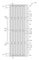
Please refer to FIG. 2, which is a plan view of a conventional memory cell array layout configuration of the SRAM. As shown in FIG. 2, each memory cell 100, which is indicated as an area enclosed by a dotted line is formed on the P+ regions 120 and the N+ region 122 between the two adjacent P+ regions 120. It should be noted that the P+ regions 120 and the N+ regions 122 are all indicated as areas enclosed by thin solid lines. Furthermore, a row of strapping cells (not shown) are positioned between two rows of the memory cells 100 for power feeding. The strapping cells include a plurality of P+ regions 130 and a plurality of N+ regions 132, which are indicated as areas enclosed by thick solid lines. The P+ regions 130 are formed simultaneously with the P+ regions 120 and the N+ regions 132 are formed simultaneously with the N+ regions 122. As shown in FIG. 2, the P+ regions 130 and the N+ regions 122 in a same column are alternately arranged. In the same concept, the N+ regions 132 and the P+ regions 120 in a same column are alternately arranged. Furthermore, the P+ regions 130 and the N+ regions 132 in the same row are alternately arranged.
Additionally, a plurality of diffusion regions (not shown) respectively serving as the source/drain regions of the n-channel MOS transistors and the p-channel MOS transistors are formed in the P+ regions 120 and the N+ regions 122. Also a plurality of diffusion regions 140 is respectively formed in the P+ regions 130 and the N+ regions 132. As shown in FIG. 2, the diffusion regions 140 is completely encompassed by the P+ regions 130 and the N+ regions 132.
It is noteworthy that with a trend toward higher integration of integrated circuit, semiconductor devices such as the memory cells 100 keep shrinking. However, it is found that the memory cell array 200 cannot be shrunk as expected. It is noteworthy that in the prior art memory cell array 200, the P+ regions 120, the N+ regions 122, the P+ regions 130, and the N+ regions 132 are all islanding configurations. Furthermore, the P+ region 130 must be kept from the corner of the P+ regions 120 by a spacing distance d1 which satisfies with the topological layout rules (TLR), and the N+ region 132 must be kept from the corner of the N+ regions 122 by a spacing distance d2 which satisfies with the TLR. In other words, the spacing distances d1 and d2 cannot be reduced in order to be compliant with the fabricator's TLR, and thus the size of the memory cell array 200 cannot be shrunk. Not only the spacing distances d1 and d2 cannot be reduced, but also the size of the P+ regions 130 and the N+ regions 132 cannot be shrunk due to optical limitations. Furthermore, it is found that the layout configuration of the conventional memory cell array 200 has many TLR design rule check (DRC) violation and causes many risks such as incomplete opening in masking layer for forming the P+ regions 130, the N+ regions 132, and even the diffusion regions 140, and causes inferior implantation result. As such, a layout configuration allowing memory cell array shrinking is still in need.
SUMMARY OF THE INVENTION
According to an aspect of the present invention, a layout configuration for a memory cell array is provided. The layout configuration includes at least a comb-like doped region having a first conductivity type and a fishbone-shaped doped region having a second conductivity type. The second conductivity type and the first conductivity type are complementary. More important, the comb-like doped region and the fishbone-shaped doped region are interdigitated.
According to another aspect of the present invention, a layout configuration for a memory cell array is provided. The layout configuration for a memory cell array includes a top area, a bottom area, and a plurality of gap areas defined in between the top area and the bottom area; a pair of comb-like doped regions having a first conductivity type respectively formed in the top area and the bottom area; at least a first fishbone-shaped doped region having a second conductivity type formed in the gap areas; and at least a second fishbone-shaped doped region having the first conductivity type formed in the gap areas. The second conductivity type and the first conductivity type are complementary
According to the layout configurations for a memory cell array provided by the present invention, the comb-like doped regions and the fishbone-shaped regions in which the memory cells and the strap cell are formed are provided. Specifically speaking, the strap cells are formed in the base portions of the comb-like doped regions and the stem-like portions of the fishbone-shaped doped regions while the memory cells are formed in the tooth portions of the comb-like doped regions and the branch-like portions of the fishbone-shaped regions. Therefore no spacing distance is needed between the doped regions for forming the strap cells and the doped regions for forming the memory cells. Accordingly the memory cell array provided by the present invention can be shrunk as expected.
These and other objectives of the present invention will no doubt become obvious to those of ordinary skill in the art after reading the following detailed description of the preferred embodiment that is illustrated in the various figures and drawings.
BRIEF DESCRIPTION OF THE DRAWINGS
FIG. 1 is a plan view of a conventional memory cell layout of a 6T-SRAM.
FIG. 2 is a plan view of a conventional memory cell array layout of the SRAM.
FIG. 3 is a decomposition view of a layout configuration for a memory cell array provided by a first preferred embodiment of the present invention.
FIG. 4 is another decomposition view of the layout configuration for a memory cell array provided by the first preferred embodiment.
FIG. 5 is still another decomposition view of the layout configuration for a memory cell array provided by the first preferred embodiment.
FIG. 6 is a schematic plan view of the layout configuration for a memory cell array provided by the first preferred embodiment.
FIG. 7 is a schematic plan view of the layout configuration for a memory cell array provided by a second preferred embodiment of the present invention.
DETAILED DESCRIPTION
Please refer to FIGS. 3-6, wherein FIG. 3 is a decomposition view of a layout configuration for a memory cell array provided by a first preferred embodiment of the present invention, FIG. 4 is another decomposition view of the layout configuration for a memory cell array provided by the first preferred embodiment, FIG. 5 is still another decomposition view of the layout configuration for a memory cell array provided by the first preferred embodiment, and FIG. 6 is a schematic plan view of the layout configuration provided by the first preferred embodiment.
As shown in FIG. 3, the layout configuration 300 for a memory cell array provided by the preferred embodiment includes at least a comb-like doped region 310, preferably a pair of comb-like doped regions 310, having a first conductivity type. The comb-like doped region 310 includes a base portion 312 and a plurality of tooth portions 314. The base portion 312 extends along a first direction while the tooth portions 314 extend along a second direction. In this preferred embodiment, the first direction and the second direction are perpendicular to each other.
Please refer to FIG. 4. The layout configuration 300 for a memory cell array provided by the preferred embodiment also includes a fishbone-shaped doped region 320 having a second conductivity type. The second conductivity type and the first conductivity type are complementary. In this preferred embodiment, the first conductivity type is p type and the second conductivity type is n type. The fishbone-shaped doped region 320 includes a stem-like portion 322 and a plurality of branch-like portions 324 while the branch-like portions 324 are symmetrical about the stem-like portion 322. The stem-like portion 322 extends along the first direction and the branch-like portions 324 extend along the second direction.
Please refer to FIG. 5. Please note that the comb-like doped regions 310 are filled with slash (“/”) pattern and the fishbone-shaped doped region 320 is filled with backslash (“\”) pattern for differentiating from each other and emphasizing. As shown in FIG. 5, the comb-like doped regions 310 and the fishbone-shaped doped region 320 are interdigitated. Specifically speaking, the tooth portions 314 of the comb-like doped region 310 and the branch-like portions 324 of the fishbone-shaped doped region 320 are interdigitated. In other words, the tooth portions 314 and the branch-like portions 324 are alternately arranged. Additionally, the base portions 312 of the comb-like doped regions 310 and the stem-like portion 322 of the fishbone-shaped doped region 320 are parallel with each other. It is noteworthy that the branch-like portions 324 of the fishbone-shaped doped region 320 and the tooth portions 314 of the comb-like doped region 310 are the places where the memory cells (not shown) are to be formed. As mentioned above, a memory cell includes two p-channel MOS transistors (now shown) formed in the branch-like portions 324 of the fishbone-shaped doped region 320 and four n-channel MOS transistors (not shown) formed in the tooth portions 314 of the comb-like doped regions 310.
Additionally, a plurality of n-type diffusion regions (not shown) respectively serving as the source/drain regions of the n-channel MOS transistor device is formed in the tooth portions 314 of the comb-like doped region 310 and a plurality of p-type diffusion regions (not shown) respectively serving as the source/drain regions of the p-channel MOS transistor device is formed in the branch portions 324 of the fishbone-shaped doped region 320. Though those diffusion regions are omitted for simplifying the drawings and avoiding confusion, those skilled in the art should easily realize that those diffusion regions cannot be ignored from the memory array.
Please refer to FIG. 6. The layout configuration 300 provided by the preferred embodiment further includes a plurality of first diffusion regions 316 formed in the base portion 312 of the comb-like doped region 310. The layout configuration 300 also includes a plurality of second diffusion regions 326 formed in the stem-like portion 322 of the fishbone-shaped doped region 320. The first diffusion regions 316 and the second diffusion regions 326 are all indicated as an area enclosed by a dotted line. The first diffusion regions 316 include the second conductivity and the second diffusion regions 326 include the first conductivity. It is noteworthy that the strap cells, which are provided for power feeding, include the first diffusion regions 316 for the n-channel MOS transistor device and the second diffusion regions 326 for the p-channel MOS transistor device.
According to the layout configuration for a memory cell array provided by the present invention, the doped regions in which the memory cells are produced and the doped regions in which the strap cells are produced are no longer islanding configurations. Instead, the doped regions having the same conductivity type are formed as a continuous configuration, such as the comb-like doped regions 310 and the fishbone-shaped doped region 320. Specifically speaking, the strap cells are formed in the base portions 312 of the comb-like doped regions 310 and the stem-like portion 322 of the fishbone-shaped doped region 320 while the memory cells are formed in the tooth portions 314 of the comb-like doped regions 310 and the branch-like portions 324 of the fishbone-shaped regions 320. Consequently, no spacing distance is needed anymore. Accordingly the memory cell array 300 provided by the present invention can be shrunk as expected.
Secondly, it is well-known that diffusion regions must be formed within the islanding doped regions in the prior art, and thus the size of the diffusion regions is limited by the conventional islanding doped regions and cannot be enlarged for improving implantation result. As a countermeasure against to this problem, the diffusion regions 316 of the preferred embodiment are formed in the base portions 314 of the comb-like doped region 310 and diffusion regions 326 of the preferred embodiment are formed in the stem-like portion 322 of the fishbone-shaped doped region 320. It is observed that the diffusion regions 316 and 326 are formed in the continuous configurations without spacing distance required. Thus the size of the diffusion regions 316 and 326 can be enlarged as shown in FIG. 6. Additionally, a shape of the diffusion regions 316 and 326 can be a rectangle with its long sides parallel with the extending direction of the base portions 312 of the comb-like doped region 310 and the stem-like portion 322 of the fishbone-shaped doped region 320, but not limited to this. Consequently, when forming the masking layer having openings for defining the diffusion regions 316 and 326, the openings are formed with superior profile since the designed diffusion regions 316/326 are enlarged. Therefore, ion implantation results for forming the diffusion regions 316 and 326 are improved.
Please refer to FIG. 7, which is a schematic plan view of a layout configuration for a memory cell array provided by a second preferred embodiment. Please note that elements the same in both of the first and second preferred embodiments are designated by the same numerals. The layout configuration 300 for a memory cell array provided by the preferred embodiment includes a top area 302, a bottom area 304, and a plurality of memory cell areas 306 defined between the top area 302 and the bottom area 304. More important, the layout configuration 300 further includes a plurality of gap areas 308 defined between the top area 302 and the bottom area, particularly between the memory cell areas 306. In other words, the memory cell areas 306 are interrupted by the gap areas 308 as shown in FIG. 7. It should be easily realized that the amounts of the memory cell areas 306 and the gap areas 308 can be repeated any number of times to feed the needs. Although not shown in the figures, it will be appreciated by those of ordinary skill in the art that a plurality of memory cells are arranged in matrix in each of the memory cell areas 306. Since the arrangement of the memory cells are well-known to those skilled in the art, the memory cells formed in the memory cell areas 306 are all omitted for simplicity.
Please refer to FIG. 7 again. The layout configuration 300 for a memory cell array provided by the preferred embodiment also includes a pair of comb-like doped regions 310 having a first conductivity type respectively formed in the top area 302 and the bottom area 304. Each of the comb-like doped regions 310 includes a base portion 312 and a plurality of tooth portions 314. As shown in FIG. 7, the comb-like doped regions 310 in one pair are mirror symmetric to each other, therefore the base portion 312 of one comb-like doped region 310 is formed in the top area 302 and base portion 312 of the other comb-like doped region 310 is formed in the bottom area 304. Additionally, the tooth portions 314 of the pair of the comb-like doped regions 310 extend into the memory cell areas 306, and the memory cells are formed in the tooth portions 314 of the comb-like doped regions 310.
The layout configuration 300 for a memory cell array of the preferred embodiment also includes a plurality of first fishbone-shaped doped regions 320 a and a plurality of second fishbone-shaped doped region 320 b. The first fishbone-shaped doped region 320 a includes a second conductivity type while the second fishbone-shaped doped region 320 b includes the first conductivity type. The second conductivity type and the first conductivity type are complementary. In this preferred embodiment, the first conductivity type is a p type and the second conductivity type is an n type. As shown in FIG. 7, at least two first fishbone-shaped doped regions 320 a are adjacent to the pair of the comb-like doped regions 310. The first fishbone-shaped doped regions 320 a and the comb-like doped regions 310 are interdigitated. Also, the first fishbone-shaped doped regions 320 a and the second fishbone-shaped doped regions 320 b are interdigitated.
Please still refer to FIG. 7. The first fishbone-shaped doped region 320 a includes a first stem-like portion 322 a and a plurality of first branch-like portions 324 a while the first branch-like portions 324 a are symmetrical about the first stem-like portion 322 a. The first stem-like portions 322 a are formed in the gap areas 308 and the first branch-like portions 324 a extend into the memory cell area 306. The second fishbone-shaped doped region 320 b includes a second stem-like portion 322 b and a plurality of second branch-like portions 324 b while the second branch-like portions 324 b are symmetrical about the second stem-like portion 322 b. The second stem-like portions 322 b are formed in the gap areas 308 and the second branch-like portions 324 b extend into the memory cell area 306. As shown in FIG. 7, the base portions 312 of the comb-like doped regions 310, the first stem-like portions 322 a of the first fishbone-shaped doped regions 320 a, and the second stem-like portions 322 b of the second fishbone-shaped doped region 320 b are parallel with each other. It is noteworthy that according to the present preferred embodiment, the tooth portions 314 of the comb-like doped region 310 and the first branch-like portions 324 a of the first fishbone-shaped doped region 320 a are alternately arranged, and the first branch-like portions 324 a of the first fishbone-shaped doped region 320 a and the second branch-like portion 324 b of the second fishbone-shaped doped region 320 b are alternately arranged. It is ensured that in the memory cell areas 306, the doped regions having the first conductivity type are all adjacent to the doped regions having the second conductivity type.
The layout configuration 300 for a memory cell array provided by the preferred embodiment further includes a plurality of n-type diffusion regions (not shown) respectively serving as the source/drain regions of the n-channel MOS transistor device formed in the tooth portions 314 of the comb-like doped regions 310, a plurality of n-type diffusion regions (not shown) respectively serving as the source/drain regions of the p-channel MOS transistor device formed in the first branch portions 324 a of the first fishbone-shaped doped regions 320, and a plurality of p-type diffusion regions formed in the second branch-like portions 324 b of the second fishbone-shaped doped regions 320 b. Though those diffusion regions are omitted for simplifying the drawings and avoiding confusion, those skilled in the art should easily realize that those diffusion regions cannot be ignored from the memory cell array.
More important, the layout configuration 300 provided by the preferred embodiment further includes a plurality of first diffusion regions 316 formed in the base portions 312 of the comb-like doped regions 310. The first diffusion regions 316 include the second conductivity type. Also, the layout configuration 300 includes a plurality of second diffusion regions 326 a formed in the second stem-like portions 322 b of the second fishbone-shaped doped regions 320 b and a plurality of third diffusion regions 326 b formed in the first stem-like portions 324 a of the first fishbone-shaped doped regions 320 a. The second diffusion regions 326 a include the second conductivity type and the third diffusion regions 326 b include the first conductivity type. The first diffusion regions 316, the second diffusion regions 326 a and the third diffusion regions 326 b are all indicated as an area enclosed by a dotted line. It is noteworthy that the strap cells, which are provided for power feeding, include the first diffusion regions 316 for the n-channel MOS transistors, the second diffusion regions 326 a for the n-channel MOS transistors, and the third diffusion regions 326 b for the p-channel MOS transistors.
It is well-known that conventional homogenous memory cells are always interrupted by the strap cell in order to provide a required minimum potential for all cells in the memory cell areas 306, therefore the preferred embodiment provides the doped regions (the tooth portions 314, the first branch-like portions 324 a, and the second branch-like portions 324 b) in which the memory cells are produced and the doped regions (the base portions 312, the first stem-like portions 322 a, and the second stem-like portions 322 b) in which the strap cells are produced. Different from the prior art, the doped regions having the same conductivity are no longer islanding configurations, but are formed as a continuous configuration, such as the comb-like doped region 310, the first fishbone-shaped doped region 320 a, and the second fishbone-shaped doped region 320 b. Consequently, no spacing distance is needed anymore, and thus the memory cell array 300 provided by the present invention can be further shrunk. In the same time, since the diffusion regions 316/326 a/326 b are formed in the continuous configurations without spacing distance required. Thus the size of the diffusion regions 316/326 a/326 b can be enlarged as shown in FIG. 7. Consequently, ion implantation results for forming the diffusion regions 316/326 a/326 b are improved.
According to the layout configurations for a memory cell array provided by the present invention, the comb-like doped regions and the fishbone-shaped regions in which the memory cells and the strap cell are formed are provided. Specifically speaking, the strap cells are formed in the base portions of the comb-like doped regions and the stem-like portions of the fishbone-shaped doped regions while the memory cells are formed in the tooth portions of the comb-like doped regions and the branch-like portions of the fishbone-shaped regions. Therefore no spacing distance is needed between the doped regions for forming the strap cells and the doped regions for forming the memory cells. Accordingly the memory cell array provided by the present invention can be shrunk as expected.
Those skilled in the art will readily observe that numerous modifications and alterations of the device and method may be made while retaining the teachings of the invention. Accordingly, the above disclosure should be construed as limited only by the metes and bounds of the appended claims.

Claims (11)

What is claimed is:
1. A layout configuration for a memory cell array comprising:
a top area, a bottom area, and a plurality of gap areas defined between the bottom area and the bottom area;
a pair of comb-like doped layers having a first conductivity type respectively formed in the top area and the bottom area;
a dual fishbone layer comprising at least a first fishbone-shaped doped region having a second conductivity type formed in the gap areas, the second conductivity type and the first conductivity type being complementary; and
at least a second fishbone-shaped doped layer having the first conductivity type formed in the gap areas, wherein the comb-like doped layers are physically contacted with the first fishbone-shaped doped region, and the first fishbone-shaped doped region is physically contacted with the second fishbone-shaped doped layer.
2. The layout configuration for a memory cell array according to claim 1, wherein the comb-like doped layers comprises a plurality of tooth portions and a base portion, and the base portions of the comb-like doped layers are formed in the top area and the bottom area.
3. The layout configuration for a memory cell array according to claim 2, further comprising a plurality of first diffusion regions formed in the base portions of the comb-like doped layers.
4. The layout configuration for a memory cell array according to claim 3, wherein the first diffusion regions comprise the second conductivity type.
5. The layout configuration for a memory cell array according to claim 2, wherein the first fishbone-shaped doped region comprises a plurality of first branch-like portions and a first stem-like portion, and the second fishbone-shaped doped layer comprises a plurality of second branch-like portions and a second stem-like portion.
6. The layout configuration for a memory cell array according to claim 5, wherein the base portions of the comb-like doped layers, the first stem-like portion of the first fishbone-shaped doped region, and the second stem-like portion of the second fishbone-shaped doped layer are parallel with each other.
7. The layout configuration for a memory cell array according to claim 5, wherein the tooth portions of the comb-like doped layers and the first branch-like portions of the first fishbone-shaped doped region are alternately arranged, and the first branch-like portions of the first fishbone-shaped doped region and the second branch-like portions of the second fishbone-shaped doped layer are alternately arranged.
8. The layout configuration for a memory cell array according to claim 5, further comprising a plurality of second diffusion regions formed in the second stem-like portion of the second fishbone-shaped doped layer, the second diffusion regions comprise the second conductivity type.
9. The layout configuration for a memory cell array according to claim 5, further comprising a plurality of third diffusion regions formed in the first stem-like portion of the first fishbone-shaped doped region, the third diffusion regions comprise the first conductivity type.
10. The layout configuration for a memory cell array according to claim 1, wherein the first fishbone-shaped doped region is adjacent to one of the comb-like doped layers and the first fishbone-shaped doped region and one of the comb-like doped layers are interdigitated.
11. The layout configuration for a memory cell array according to claim 10, wherein the first fishbone-shaped doped region and the second fishbone-shaped doped layer are interdigitated.
US13/287,141 2011-11-02 2011-11-02 Layout configuration for memory cell array Active 2031-12-21 US8614463B2 (en)

Priority Applications (2)

Application Number Priority Date Filing Date Title
US13/287,141 US8614463B2 (en) 2011-11-02 2011-11-02 Layout configuration for memory cell array
US14/062,914 US9166003B2 (en) 2011-11-02 2013-10-25 Layout configuration for memory cell array

Applications Claiming Priority (1)

Application Number Priority Date Filing Date Title
US13/287,141 US8614463B2 (en) 2011-11-02 2011-11-02 Layout configuration for memory cell array

Related Child Applications (1)

Application Number Title Priority Date Filing Date
US14/062,914 Continuation US9166003B2 (en) 2011-11-02 2013-10-25 Layout configuration for memory cell array

Publications (2)

Publication Number Publication Date
US20130105864A1 US20130105864A1 (en) 2013-05-02
US8614463B2 true US8614463B2 (en) 2013-12-24

Family

ID=48171489

Family Applications (2)

Application Number Title Priority Date Filing Date
US13/287,141 Active 2031-12-21 US8614463B2 (en) 2011-11-02 2011-11-02 Layout configuration for memory cell array
US14/062,914 Active 2031-11-30 US9166003B2 (en) 2011-11-02 2013-10-25 Layout configuration for memory cell array

Family Applications After (1)

Application Number Title Priority Date Filing Date
US14/062,914 Active 2031-11-30 US9166003B2 (en) 2011-11-02 2013-10-25 Layout configuration for memory cell array

Country Status (1)

Country Link
US (2) US8614463B2 (en)

Cited By (1)

* Cited by examiner, † Cited by third party
Publication number Priority date Publication date Assignee Title
TWI656622B (en) * 2014-09-23 2019-04-11 聯華電子股份有限公司 Integrated circuit layout structure

Families Citing this family (1)

* Cited by examiner, † Cited by third party
Publication number Priority date Publication date Assignee Title
CN105321886B (en) * 2014-05-29 2019-07-05 联华电子股份有限公司 Capacitor structure and manufacturing method thereof

Citations (3)

* Cited by examiner, † Cited by third party
Publication number Priority date Publication date Assignee Title
US4406710A (en) * 1981-10-15 1983-09-27 Davies Roderick D Mask-saving technique for forming CMOS source/drain regions
US6049113A (en) * 1997-06-05 2000-04-11 Nec Corporation Semiconductor device and semiconductor device manufacturing method
US20060261400A1 (en) * 2005-05-17 2006-11-23 Nec Electronics Corporation Nonvolatile semiconductor device

Patent Citations (3)

* Cited by examiner, † Cited by third party
Publication number Priority date Publication date Assignee Title
US4406710A (en) * 1981-10-15 1983-09-27 Davies Roderick D Mask-saving technique for forming CMOS source/drain regions
US6049113A (en) * 1997-06-05 2000-04-11 Nec Corporation Semiconductor device and semiconductor device manufacturing method
US20060261400A1 (en) * 2005-05-17 2006-11-23 Nec Electronics Corporation Nonvolatile semiconductor device

Cited By (1)

* Cited by examiner, † Cited by third party
Publication number Priority date Publication date Assignee Title
TWI656622B (en) * 2014-09-23 2019-04-11 聯華電子股份有限公司 Integrated circuit layout structure

Also Published As

Publication number Publication date
US9166003B2 (en) 2015-10-20
US20140035111A1 (en) 2014-02-06
US20130105864A1 (en) 2013-05-02

Similar Documents

Publication Publication Date Title
US10522554B2 (en) SRAM cells with vertical gate-all-around MOSFETs
KR101161506B1 (en) Cell structure for dual port SRAM
US9317646B2 (en) Masks formed based on integrated circuit layout design having cell that includes extended active region
US8315084B2 (en) Fully balanced dual-port memory cell
US7889540B2 (en) Semiconductor device including memory having nodes connected with continuous diffusion layer but isolated from each other by transistor
US8860096B2 (en) Semiconductor devices including SRAM cell and methods for fabricating the same
US20140312427A1 (en) Semiconductor Devices Having Fin Shaped Channels
KR20150056518A (en) Sram cells and arrays
US11640962B2 (en) Semiconductor structure
KR100882549B1 (en) Semiconductor memory
US10734372B2 (en) Vertical transport static random-access memory cells with transistors of active regions arranged in linear rows
US11315624B2 (en) Semiconductor memory device
US20240038755A1 (en) Semiconductor structure of cell array
US8614463B2 (en) Layout configuration for memory cell array
US20250151391A1 (en) Logic cell with small cell delay
JP2006269674A (en) Semiconductor integrated circuit
US20140054716A1 (en) SRAM Cells with Dummy Insertions
US20230178537A1 (en) Semiconductor structure of hybrid cell array
US20170250197A1 (en) Layout structure for semiconductor integrated circuit
US20230178557A1 (en) Semiconductor structure of logic cell with small cell delay
CN106653755A (en) Static random access memory
US9484349B1 (en) Static random access memory
US20090067219A1 (en) Semiconductor memory device including SRAM cell having well power potential supply region provided therein
US20240038760A1 (en) Integrated circuit cell with dual row, back-to-back, transistor body ties
CN112259535A (en) Finfet process-based basic digital logic unit and integrated circuit layout

Legal Events

Date Code Title Description
AS Assignment

Owner name: UNITED MICROELECTRONICS CORP., TAIWAN

Free format text: ASSIGNMENT OF ASSIGNORS INTEREST;ASSIGNORS:CHUANG, MENG-PING;KUO, YU-TSE;SUN, CHIA-CHUN;AND OTHERS;REEL/FRAME:027158/0219

Effective date: 20110908

STCF Information on status: patent grant

Free format text: PATENTED CASE

FPAY Fee payment

Year of fee payment: 4

MAFP Maintenance fee payment

Free format text: PAYMENT OF MAINTENANCE FEE, 8TH YEAR, LARGE ENTITY (ORIGINAL EVENT CODE: M1552); ENTITY STATUS OF PATENT OWNER: LARGE ENTITY

Year of fee payment: 8

MAFP Maintenance fee payment

Free format text: PAYMENT OF MAINTENANCE FEE, 12TH YEAR, LARGE ENTITY (ORIGINAL EVENT CODE: M1553); ENTITY STATUS OF PATENT OWNER: LARGE ENTITY

Year of fee payment: 12