US8613825B2 - Method for fixing glass substrates and method for preparing flexible display device - Google Patents
Method for fixing glass substrates and method for preparing flexible display device Download PDFInfo
- Publication number
- US8613825B2 US8613825B2 US13/407,849 US201213407849A US8613825B2 US 8613825 B2 US8613825 B2 US 8613825B2 US 201213407849 A US201213407849 A US 201213407849A US 8613825 B2 US8613825 B2 US 8613825B2
- Authority
- US
- United States
- Prior art keywords
- glass substrate
- epoxy resin
- glass
- annealing
- glass substrates
- Prior art date
- Legal status (The legal status is an assumption and is not a legal conclusion. Google has not performed a legal analysis and makes no representation as to the accuracy of the status listed.)
- Expired - Fee Related, expires
Links
Images


Classifications
-
- C—CHEMISTRY; METALLURGY
- C03—GLASS; MINERAL OR SLAG WOOL
- C03B—MANUFACTURE, SHAPING, OR SUPPLEMENTARY PROCESSES
- C03B25/00—Annealing glass products
- C03B25/04—Annealing glass products in a continuous way
- C03B25/06—Annealing glass products in a continuous way with horizontal displacement of the glass products
- C03B25/08—Annealing glass products in a continuous way with horizontal displacement of the glass products of glass sheets
-
- C—CHEMISTRY; METALLURGY
- C03—GLASS; MINERAL OR SLAG WOOL
- C03C—CHEMICAL COMPOSITION OF GLASSES, GLAZES OR VITREOUS ENAMELS; SURFACE TREATMENT OF GLASS; SURFACE TREATMENT OF FIBRES OR FILAMENTS MADE FROM GLASS, MINERALS OR SLAGS; JOINING GLASS TO GLASS OR OTHER MATERIALS
- C03C27/00—Joining pieces of glass to pieces of other inorganic material; Joining glass to glass other than by fusing
- C03C27/06—Joining glass to glass by processes other than fusing
-
- Y—GENERAL TAGGING OF NEW TECHNOLOGICAL DEVELOPMENTS; GENERAL TAGGING OF CROSS-SECTIONAL TECHNOLOGIES SPANNING OVER SEVERAL SECTIONS OF THE IPC; TECHNICAL SUBJECTS COVERED BY FORMER USPC CROSS-REFERENCE ART COLLECTIONS [XRACs] AND DIGESTS
- Y02—TECHNOLOGIES OR APPLICATIONS FOR MITIGATION OR ADAPTATION AGAINST CLIMATE CHANGE
- Y02P—CLIMATE CHANGE MITIGATION TECHNOLOGIES IN THE PRODUCTION OR PROCESSING OF GOODS
- Y02P40/00—Technologies relating to the processing of minerals
- Y02P40/50—Glass production, e.g. reusing waste heat during processing or shaping
- Y02P40/57—Improving the yield, e-g- reduction of reject rates
-
- Y—GENERAL TAGGING OF NEW TECHNOLOGICAL DEVELOPMENTS; GENERAL TAGGING OF CROSS-SECTIONAL TECHNOLOGIES SPANNING OVER SEVERAL SECTIONS OF THE IPC; TECHNICAL SUBJECTS COVERED BY FORMER USPC CROSS-REFERENCE ART COLLECTIONS [XRACs] AND DIGESTS
- Y10—TECHNICAL SUBJECTS COVERED BY FORMER USPC
- Y10T—TECHNICAL SUBJECTS COVERED BY FORMER US CLASSIFICATION
- Y10T156/00—Adhesive bonding and miscellaneous chemical manufacture
- Y10T156/11—Methods of delaminating, per se; i.e., separating at bonding face
- Y10T156/1111—Using solvent during delaminating [e.g., water dissolving adhesive at bonding face during delamination, etc.]
- Y10T156/1116—Using specified organic delamination solvent
Definitions
- Embodiments of the disclosed technology relate to a method for fixing glass substrates and a method for preparing a flexible display device.
- LCDs liquid crystal displays
- CTR cathode ray tube
- a flexible display device has characteristics of bendability, which enables it suitable for many applications in need of curved display, such as smart card, e-paper, smart tags, and applications suitable for conventional displays. Furthermore, in the future, flexible display devices may take an enormous market share in the field of panel display products with its fantastic beautiful appearance.
- flexible display devices are mainly manufactured based on organic material substrates, for example, cholesteric phase LCD, electrophoresis display, and OLED (Organic Light-Emitting Display) or the like manufactured on organic substrates such as polyimide, polythylene terephthalate films (PET), polyethylene terephthalate (PETP) and the like.
- organic substrates such as polyimide, polythylene terephthalate films (PET), polyethylene terephthalate (PETP) and the like.
- PET polythylene terephthalate films
- PETP polyethylene terephthalate
- Glass substrates are superior to organic material substrates in light transmittance, chemical stability, water-proof capability and dielectric performance; moreover, ultrathin glass substrates also have good flexibility; however, because of the fragility of glass substrates, the application of glass substrates in large-size screen panel display products is remarkably limited, and it is also very difficult to separately transfer and process ultrathin glass substrates.
- An embodiment of the disclosed technology provides a method for fixing glass substrates, which shortens the time period for fixing the adhered glass substrates while improving productivity.
- An embodiment of the disclosed technology provides a method for fixing glass substrates, comprising: coating an edge portion of a first glass substrate corresponding to a second glass substrate with epoxy resin and screeding the coated epoxy resin layer, wherein a thickness of the first glass substrate is bigger than that of the second glass substrate; adhering the second glass substrate to the first glass substrate with the coated epoxy resin layer; and annealing the two glass substrates after adherence.
- coating the edge portion of the first glass substrate corresponding to the second glass substrate with epoxy resin comprises: coating the edge portion of the first glass substrate corresponding to the second glass substrate with epoxy resin in a strip in a width of about 5-20 mm.
- the thickness of the first glass substrate is not less than 0.4 mm, and the thickness of the second glass substrate is not more than 0.1 mm.
- the epoxy resin is a non-photosensitive epoxy resin or photosensitive epoxy resin.
- the method may further comprise, before annealing said two glass substrates, performing exposing process on the two glass substrates.
- performing exposing process on the pair of glass substrates comprises: irradiating the two glass substrates with ultraviolet ray, and the wavelength of the ultraviolet ray is one of 365 nm, 405 nm, and 436 nm, or any combination thereof.
- annealing the two glass substrates comprises: placing the first glass substrate and the second glass substrate into an oven for annealing, wherein an annealing temperature is set in the range of about 40° C. to about 60° C., and when the epoxy resin is a photosensitive epoxy resin, a time period for annealing is set in the range of about 5 min to about 15 min, and when the epoxy resin is a non-photosensitive epoxy resin, a time period for annealing is set in the range of about 15 min to about 30 min.
- the method may further comprise: cooling the two annealed glass substrates to ambient temperature for preparing a flexible display device on the second glass substrate; and softening the coated epoxy resin and separating the first glass substrate from the second glass substrate.
- softening the coated epoxy resin and separating the first glass substrate from the second glass substrate comprises: contacting the two glass substrates coated with epoxy resin with acetone or 3M adhesive remover, and after the coated epoxy resin is softened by the acetone or 3M adhesive remover, separating the first glass substrate from the second glass substrate.
- Another embodiment of the disclosed technology provides a method for preparing a flexible display device, comprising: providing a base substrate, comprising: coating an edge portion of a first glass substrate corresponding to a second glass substrate with epoxy resin and screeding the coated epoxy resin layer, wherein a thickness of the first glass substrate is bigger than that of the second glass substrate, adhering the second glass substrate to the first glass substrate with the coated epoxy resin layer, annealing the two glass substrates after adherence, and cooling the two annealed glass substrates to ambient temperature, wherein the second glass substrate is used as the base substrate; and preparing the flexible display device on the second glass substrate as the base substrate, which is bonded to the first glass substrate.
- the method for fixing glass substrates in an embodiment of the disclosed technology enables rapid curing of epoxy resin and thereby rapid fixing together of the two glass substrates, and furthermore, no bubbles generate during the rapid curing of epoxy resin, thus assuring a good resistance effect of glass substrates against strong acid, strong base, and organic solvent and the like.
- the substrates are used for preparing flat display devices, it is possible to increase the ratio of non-defective products and productivity, thus improve the product competitiveness.
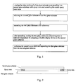
- FIG. 1 is a schematic view showing the steps of a method for fixing glass substrates of a first embodiment according to the disclosed technology
- FIG. 2 is a schematic sectional view after adhering of the first glass substrate to the second glass substrate.
- FIG. 3 is a schematic view showing the steps of a method for fixing glass substrates of a second embodiment according to the disclosed technology.
- the display devices may be subject to treatments at a high temperature above 300 degrees Celsius and dipped into strong acid solutions, strong base solutions, and organic solvents such as iso-propyl alcohol. Therefore, the binding materials for adhering need resistances to high temperature, strong acid, strong base, and organic solvent.
- Epoxy resin is one of the materials with resistances to severe circumstances such as high temperature, strong acid, strong base, organic solvent etc. for a certain period. However, in high temperature curing, epoxy resin tends to generate lots of bubbles and give rise to thermal shrinking, causing gaps and cracks in sealed boundaries, and thus liquid may enter into the space between an ultrathin glass substrate and a thicker glass substrate that are bonded together.
- an embodiment of the disclosed technology provides a method for fixing glass substrates with epoxy resin, comprising coating the edge portion of a first glass substrate corresponding to a second glass substrate with epoxy resin and leveling (or screeding) the coated epoxy resin layer, adhering the second glass substrate to the first glass substrate with the coated epoxy resin layer, and annealing the two glass substrates after adherence.
- FIG. 1 is a schematic view showing the steps of a method for fixing glass substrates of a first embodiment according to the disclosed technology, by using a non-photosensitive epoxy resin. As shown in FIG. 1 , the method of the first embodiment comprises the following steps.
- Step 101 coating the edge portion of a first glass substrate corresponding to a second glass substrate with epoxy resin and screeding the coated epoxy resin layer.
- FIG. 2 is schematic sectional view after adhering of the first glass substrate to the second glass substrate.
- an epoxy resin material is coated in a strip shape in the width of about 5 ⁇ 20 mm.
- the first glass substrate is a thicker glass substrate with a thickness of not less than 0.4 mm
- the second glass substrate is an ultrathin glass substrate with a thickness of not more than 0.1 mm.
- the epoxy resin may be sufficiently mixed with ethylenediamine used as a curing agent. Usually, the volumetric mixing ratio of epoxy resin and ethylenediamine is about 1:1.
- the epoxy resin may be in a milky white color or colorless transparent; in this embodiment, the epoxy resin is a kind of non-photosensitive epoxy resin.
- a leveling (screeding) process is performed to the coated epoxy resin material with a strickle (or a doctor blade), so as to making the thickness of the coated epoxy resin is below 0.05 mm on the first glass substrate, and the strickle may be a long ruler, a thin glass sheet and the like.
- Step 102 adhering the second glass substrate to the first glass substrate.
- Step 103 annealing the two glass substrates after adherence.
- the first glass substrate and the second glass substrate that are adhered together are placed into an oven for an annealing process.
- the annealing temperature in the oven is set in the range of about 40° C. to about 60° C.
- the time period for annealing for the non-photosensitive epoxy resin is set in the range of about 15 min to about 30 min.
- the coated epoxy resin may be changed in color, generate bubbles, or produce gaps and cracks in itself.
- the annealing temperature is too low, the used epoxy resin can not be cured completely or the curing effect is poor, thus liquid or moisture may enter into the space between the first glass substrate and the second glass substrate during the production of a flexible display device, for example.
- the time period for annealing is too long, the curing effect can not further improved greatly, but also the productivity will be adversely affected.
- Step 104 after annealing, cooling the two glass substrates adhered together to ambient temperature for preparing a flexible display device on the second glass substrate.
- the annealed first glass substrate and the second glass substrate are taken out from the annealing oven.
- a flexible display device can be made on the second glass substrate with the two glass substrates being still adhered together according to a conventional method.
- the ambient temperature is about 15 ⁇ 30° C., and preferably, the ambient temperature is about 23° C.;
- the conventional method for producing the flexible display device may comprise the steps of: firstly, a metal layer is deposited on the second glass substrate, then the two glass substrates with the metal layer are subject to an exposure process by using a photomask, an etching process, and finally a photoresist removing process, the above procedures are repeated for 4 ⁇ 6 times to obtain desired patterns (e.g., active array patterns) on a substrate.
- desired patterns e.g., active array patterns
- Step 105 softening the coated epoxy resin and separating the first glass substrate from the second glass substrate.
- the two glass substrates adhered with the coated epoxy resin is dipped into acetone or 3M adhesive remover, thus the coated epoxy resin is softened by acetone or 3M adhesive remover; and after the coated epoxy resin is softened, the first glass substrate can be separated from the second glass substrate.
- FIG. 3 is a schematic view showing the steps of a method for fixing glass substrates of a second embodiment according to the disclosed technology, in which a photosensitive epoxy resin is used. As shown in FIG. 3 , the method according to the second method comprises the following steps.
- Step 301 coating the edge portion of a first glass substrate corresponding to a second glass substrate with epoxy resin and screeding the coated epoxy resin layer.
- FIG. 2 is a schematic sectional view after adhering of the first glass substrate to the second glass substrate.
- an epoxy resin material is coated in a strip shape in the width of about 5 ⁇ 20 mm.
- the first glass substrate is a thicker glass substrate of not less than 0.4 mm in thickness
- the second glass substrate is an ultrathin one of not more than 0.1 mm in thickness.
- the epoxy resin may be sufficiently mixed with ethylenediamine used as a curing agent. Usually, the volumetric mixing ratio of epoxy resin and ethylenediamine is about 1:1.
- the epoxy resin may be in a milky white color or colorless transparent.
- the epoxy resin is a kind of photosensitive epoxy resin.
- a leveling (screeding) process is performed to the coated epoxy resin material with a strickle (or a doctor blade), so as to making the thickness of the coated epoxy resin is below 0.05 mm on the first glass substrate, and the strickle may be a long ruler, a thin glass sheet and the like.
- Step 302 adhering the second glass substrate to the first glass substrate.
- Step 303 performing exposing process on the two glass substrates.
- an exposing process is performed with respect to the two glass substrates after the second glass substrate is adhered to the first glass substrate. That is, the entirety of the two glass substrates is irradiated with ultraviolet ray.
- the wavelength of the ultraviolet ray may be one of 365 nm, 405 nm, and 436 nm, or any combination thereof.
- the intensity for exposure is determined according to the thickness of the coated epoxy resin.
- performing exposing process on the two glass substrates is an initial step for rapid curing the coated epoxy resin, so as to fix the shape of the resin.
- Step 304 annealing the two glass substrates.
- the first glass substrate and the second glass substrate after exposure are placed into an oven for annealing process, to improve the curing effect of the coated epoxy resin.
- the annealing temperature in the oven is set in the range of about 40° C. to about 60° C.
- the time period for annealing for photosensitive epoxy resin is set in the range of 5 min to 15 min.
- the temperature for annealing is too high, epoxy resin will be changed in color, generate bubbles or produce gaps and cracks in itself
- the temperature is too low, the epoxy resin can not cure completely or the curing effect is poor, thus liquid or moisture may enter into the space between the first glass substrate and the second glass substrate in the production of a flexible display device, for example.
- the time period for annealing is too long, the curing effect can not further improved greatly, but also the productivity will be adversely affected.
- the steps 305 to 306 can be performed the same as steps 104 to 105 .
- the method comprises the steps of: providing a base substrate and preparing the flexible display on the base substrate.
- the step of providing a base substrate comprises: coating an edge portion of a first glass substrate corresponding to a second glass substrate with epoxy resin and screeding the coated epoxy resin layer, wherein a thickness of the first glass substrate is bigger than that of the second glass substrate, adhering the second glass substrate to the first glass substrate with the coated epoxy resin layer, annealing the two glass substrates after adherence, and cooling the two annealed glass substrates to ambient temperature, wherein the second glass substrate is used as the base substrate.
- the flexible display device is prepared on the second glass substrate as the base substrate, which is bonded to the first glass substrate.
- the coated epoxy resin is softened and the first glass substrate is separated from the second glass substrate with the flexible display device formed thereon.
Landscapes
- Chemical & Material Sciences (AREA)
- Engineering & Computer Science (AREA)
- Materials Engineering (AREA)
- Organic Chemistry (AREA)
- Ceramic Engineering (AREA)
- Life Sciences & Earth Sciences (AREA)
- Chemical Kinetics & Catalysis (AREA)
- General Chemical & Material Sciences (AREA)
- Geochemistry & Mineralogy (AREA)
- Devices For Indicating Variable Information By Combining Individual Elements (AREA)
- Liquid Crystal (AREA)
- Electroluminescent Light Sources (AREA)
Abstract
Description
Claims (14)
Applications Claiming Priority (3)
| Application Number | Priority Date | Filing Date | Title |
|---|---|---|---|
| CN201110063833.9 | 2011-03-16 | ||
| CN201110063833 | 2011-03-16 | ||
| CN201110063833.9A CN102674669B (en) | 2011-03-16 | 2011-03-16 | Fixing method for glass substrates |
Publications (2)
| Publication Number | Publication Date |
|---|---|
| US20120234480A1 US20120234480A1 (en) | 2012-09-20 |
| US8613825B2 true US8613825B2 (en) | 2013-12-24 |
Family
ID=46807308
Family Applications (1)
| Application Number | Title | Priority Date | Filing Date |
|---|---|---|---|
| US13/407,849 Expired - Fee Related US8613825B2 (en) | 2011-03-16 | 2012-02-29 | Method for fixing glass substrates and method for preparing flexible display device |
Country Status (2)
| Country | Link |
|---|---|
| US (1) | US8613825B2 (en) |
| CN (1) | CN102674669B (en) |
Families Citing this family (4)
| Publication number | Priority date | Publication date | Assignee | Title |
|---|---|---|---|---|
| CN102674669B (en) * | 2011-03-16 | 2014-12-03 | 京东方科技集团股份有限公司 | Fixing method for glass substrates |
| TWI596071B (en) * | 2015-08-25 | 2017-08-21 | 友達光電股份有限公司 | Display panel and method for manufacturing the same |
| JP6531319B2 (en) * | 2016-05-16 | 2019-06-19 | 株式会社Nsc | Display device manufacturing method |
| CN107357064A (en) * | 2017-06-14 | 2017-11-17 | 合肥市惠科精密模具有限公司 | A kind of fixing means of TFT LCD glass substrates |
Citations (21)
| Publication number | Priority date | Publication date | Assignee | Title |
|---|---|---|---|---|
| US4470858A (en) * | 1982-12-06 | 1984-09-11 | Deltaglass S.A. | Lamination process and apparatus |
| US4510190A (en) * | 1982-03-30 | 1985-04-09 | Interpane Entwicklungs-Und Beratungsgesellschaft Mgh & Co. K.G. | Transparent, heat-insulating coating for a transparent substrate |
| US4839557A (en) * | 1987-12-18 | 1989-06-13 | Gte Products Corporation | Fill member for electroluminescent panels |
| US5066112A (en) * | 1989-12-21 | 1991-11-19 | Donnelly Corporation | Perimeter coated, electro-optic mirror |
| US5137770A (en) * | 1989-10-12 | 1992-08-11 | Sika Ag, Vorm. Kasper Winkler & Co. | Glass body containing a material for adhesion, and processes for its production and application |
| US5575577A (en) * | 1993-04-30 | 1996-11-19 | Canon Denshi Kabushiki Kaisha | Recording apparatus having position detecting device |
| US5670966A (en) * | 1994-12-27 | 1997-09-23 | Ppg Industries, Inc. | Glass antenna for vehicle window |
| US5710655A (en) * | 1993-07-21 | 1998-01-20 | Apeldyn Corporation | Cavity thickness compensated etalon filter |
| US5710612A (en) * | 1989-09-01 | 1998-01-20 | Semiconductor Energy Laboratory Co., Ltd. | Liquid crystal device and manufacturing method therefor with anisotropic conductive adhesive connecting glass substrate and glass auxiliary substrate |
| US5883465A (en) * | 1994-03-31 | 1999-03-16 | Nippondenso Co., Ltd. | Thin-film EL display panel having uniform display characteristics |
| US5959762A (en) * | 1996-11-08 | 1999-09-28 | Optical Coating Laboratory, Inc. | Variably adjustable contrast enhancement electrochromic panel adapted for curved display screens and methods of making and using same |
| US6031051A (en) * | 1996-07-25 | 2000-02-29 | Rohm And Haas Company | Liquid crystal displays containing spacers and methods for producing the spacer |
| US6172730B1 (en) * | 1998-03-06 | 2001-01-09 | Nec Corporation | Liquid crystal display apparatus having stepped section in glass substrate |
| US6461885B1 (en) * | 1998-10-13 | 2002-10-08 | Sony International (Europe) Gmbh | Method of fabricating and structure of an active matrix light-emitting display device |
| US6806936B2 (en) * | 2001-03-26 | 2004-10-19 | Sharp Kabushiki Kaisha | Display module including a display panel connected to a flexible wire board with an insulating protective layer extended inside the display panel |
| US20060009109A1 (en) * | 2003-04-16 | 2006-01-12 | Aitken Bruce G | Glass package that is hermetically sealed with a frit and method of fabrication |
| US20060008625A1 (en) * | 2004-07-12 | 2006-01-12 | Guardian Industries Corp. | Vehicle window unit with foam based seal and corresponding method |
| US7411230B2 (en) * | 2002-04-22 | 2008-08-12 | Fujifilm Corporation | Solid-state imaging device and method of manufacturing said solid-state imaging device |
| US7826123B2 (en) * | 2002-09-20 | 2010-11-02 | Donnelly Corporation | Vehicular interior electrochromic rearview mirror assembly |
| US20120006400A1 (en) * | 2010-07-06 | 2012-01-12 | Du Pont Apollo Limited | Solar module device and edge sealing coating method thereof |
| US20120234480A1 (en) * | 2011-03-16 | 2012-09-20 | Boe Technology Group Co., Ltd. | Method for fixing glass substrates and method for preparing flexible display device |
Family Cites Families (4)
| Publication number | Priority date | Publication date | Assignee | Title |
|---|---|---|---|---|
| JP4845129B2 (en) * | 2007-03-28 | 2011-12-28 | 国立大学法人京都大学 | Flexible substrate and manufacturing method thereof |
| JPWO2010004703A1 (en) * | 2008-07-08 | 2011-12-22 | 日東電工株式会社 | Method for manufacturing organic electroluminescence panel |
| CN101510587A (en) * | 2009-04-03 | 2009-08-19 | 清华大学 | Flexible passive organic electroluminescent device and method for preparing the same |
| CN101931058B (en) * | 2010-07-06 | 2013-03-13 | 电子科技大学 | Packaging structure and packaging method of organic electroluminescent device |
-
2011
- 2011-03-16 CN CN201110063833.9A patent/CN102674669B/en active Active
-
2012
- 2012-02-29 US US13/407,849 patent/US8613825B2/en not_active Expired - Fee Related
Patent Citations (24)
| Publication number | Priority date | Publication date | Assignee | Title |
|---|---|---|---|---|
| US4510190A (en) * | 1982-03-30 | 1985-04-09 | Interpane Entwicklungs-Und Beratungsgesellschaft Mgh & Co. K.G. | Transparent, heat-insulating coating for a transparent substrate |
| US4470858A (en) * | 1982-12-06 | 1984-09-11 | Deltaglass S.A. | Lamination process and apparatus |
| US4839557A (en) * | 1987-12-18 | 1989-06-13 | Gte Products Corporation | Fill member for electroluminescent panels |
| US5710612A (en) * | 1989-09-01 | 1998-01-20 | Semiconductor Energy Laboratory Co., Ltd. | Liquid crystal device and manufacturing method therefor with anisotropic conductive adhesive connecting glass substrate and glass auxiliary substrate |
| US5137770A (en) * | 1989-10-12 | 1992-08-11 | Sika Ag, Vorm. Kasper Winkler & Co. | Glass body containing a material for adhesion, and processes for its production and application |
| US5066112A (en) * | 1989-12-21 | 1991-11-19 | Donnelly Corporation | Perimeter coated, electro-optic mirror |
| US5575577A (en) * | 1993-04-30 | 1996-11-19 | Canon Denshi Kabushiki Kaisha | Recording apparatus having position detecting device |
| US5710655A (en) * | 1993-07-21 | 1998-01-20 | Apeldyn Corporation | Cavity thickness compensated etalon filter |
| US5883465A (en) * | 1994-03-31 | 1999-03-16 | Nippondenso Co., Ltd. | Thin-film EL display panel having uniform display characteristics |
| US5670966A (en) * | 1994-12-27 | 1997-09-23 | Ppg Industries, Inc. | Glass antenna for vehicle window |
| US6031051A (en) * | 1996-07-25 | 2000-02-29 | Rohm And Haas Company | Liquid crystal displays containing spacers and methods for producing the spacer |
| US5959762A (en) * | 1996-11-08 | 1999-09-28 | Optical Coating Laboratory, Inc. | Variably adjustable contrast enhancement electrochromic panel adapted for curved display screens and methods of making and using same |
| US6172730B1 (en) * | 1998-03-06 | 2001-01-09 | Nec Corporation | Liquid crystal display apparatus having stepped section in glass substrate |
| US6480254B1 (en) * | 1998-03-06 | 2002-11-12 | Nec Corporation | Liquid crystal display apparatus having stepped section in glass substrate |
| US6461885B1 (en) * | 1998-10-13 | 2002-10-08 | Sony International (Europe) Gmbh | Method of fabricating and structure of an active matrix light-emitting display device |
| US6806936B2 (en) * | 2001-03-26 | 2004-10-19 | Sharp Kabushiki Kaisha | Display module including a display panel connected to a flexible wire board with an insulating protective layer extended inside the display panel |
| US7411230B2 (en) * | 2002-04-22 | 2008-08-12 | Fujifilm Corporation | Solid-state imaging device and method of manufacturing said solid-state imaging device |
| US7826123B2 (en) * | 2002-09-20 | 2010-11-02 | Donnelly Corporation | Vehicular interior electrochromic rearview mirror assembly |
| US8277059B2 (en) * | 2002-09-20 | 2012-10-02 | Donnelly Corporation | Vehicular electrochromic interior rearview mirror assembly |
| US20060009109A1 (en) * | 2003-04-16 | 2006-01-12 | Aitken Bruce G | Glass package that is hermetically sealed with a frit and method of fabrication |
| US7602121B2 (en) * | 2003-04-16 | 2009-10-13 | Corning Incorporated | Glass package that is hermetically sealed with a frit and method of fabrication |
| US20060008625A1 (en) * | 2004-07-12 | 2006-01-12 | Guardian Industries Corp. | Vehicle window unit with foam based seal and corresponding method |
| US20120006400A1 (en) * | 2010-07-06 | 2012-01-12 | Du Pont Apollo Limited | Solar module device and edge sealing coating method thereof |
| US20120234480A1 (en) * | 2011-03-16 | 2012-09-20 | Boe Technology Group Co., Ltd. | Method for fixing glass substrates and method for preparing flexible display device |
Also Published As
| Publication number | Publication date |
|---|---|
| CN102674669B (en) | 2014-12-03 |
| CN102674669A (en) | 2012-09-19 |
| US20120234480A1 (en) | 2012-09-20 |
Similar Documents
| Publication | Publication Date | Title |
|---|---|---|
| CN102636898B (en) | Manufacturing method of flexible display devices | |
| US8323066B2 (en) | Method of manufacturing flexible display device | |
| US9188813B2 (en) | Liquid crystal display panel and manufacturing method thereof | |
| US20130093697A1 (en) | Touch panel display and assembly process thereof | |
| US20110255034A1 (en) | Display device | |
| TWI533034B (en) | Soft color filter and method for manufacturing soft color display element | |
| CN106773206A (en) | The manufacture method of display panel | |
| CN103064209A (en) | Method for preparing liquid crystal display panel | |
| US8613825B2 (en) | Method for fixing glass substrates and method for preparing flexible display device | |
| US20170192266A1 (en) | Method of manufacturing display panel, display panel, and display device | |
| US20090022909A1 (en) | Adhesion composition, making method of adhesion composition, display device and making method of display device | |
| US20150234222A1 (en) | Liquid crystal display panel alignment and separation | |
| US8305543B2 (en) | Substrate for liquid crystal display and sealants at opening region with different hardness, manufacturing method thereof and panel | |
| US20160246109A1 (en) | Method for manufacturing alignment mark of cf substrate | |
| CN102690066B (en) | Fixing method of glass substrate | |
| US10802328B2 (en) | Method for manufacturing display panel and baking device for display panel | |
| KR20110052759A (en) | Flexible Display Manufacturing Method | |
| CN104898316A (en) | Manufacturing method for thin type liquid crystal panel | |
| US11342358B2 (en) | Display panel and method for manufacturing same | |
| CN102707477B (en) | Manufacturing method for liquid crystal display panel | |
| US20150188096A1 (en) | Method for manufacturing flexible oled (organic light emitting display) panel | |
| CN105676540B (en) | The production method of liquid crystal display panel | |
| US8506747B2 (en) | Liquid crystal display and manufacturing method of the same | |
| CN100454090C (en) | Method for manufacturing liquid crystal display panel | |
| CN108333818A (en) | Display panel and its manufacturing method |
Legal Events
| Date | Code | Title | Description |
|---|---|---|---|
| AS | Assignment |
Owner name: BOE TECHNOLOGY GROUP CO., LTD., CHINA Free format text: ASSIGNMENT OF ASSIGNORS INTEREST;ASSIGNORS:ZHOU, WEIFENG;XUE, JIANSHE;REEL/FRAME:027780/0565 Effective date: 20111123 |
|
| STCF | Information on status: patent grant |
Free format text: PATENTED CASE |
|
| FPAY | Fee payment |
Year of fee payment: 4 |
|
| MAFP | Maintenance fee payment |
Free format text: PAYMENT OF MAINTENANCE FEE, 8TH YEAR, LARGE ENTITY (ORIGINAL EVENT CODE: M1552); ENTITY STATUS OF PATENT OWNER: LARGE ENTITY Year of fee payment: 8 |
|
| FEPP | Fee payment procedure |
Free format text: MAINTENANCE FEE REMINDER MAILED (ORIGINAL EVENT CODE: REM.); ENTITY STATUS OF PATENT OWNER: LARGE ENTITY |
|
| LAPS | Lapse for failure to pay maintenance fees |
Free format text: PATENT EXPIRED FOR FAILURE TO PAY MAINTENANCE FEES (ORIGINAL EVENT CODE: EXP.); ENTITY STATUS OF PATENT OWNER: LARGE ENTITY |
|
| STCH | Information on status: patent discontinuation |
Free format text: PATENT EXPIRED DUE TO NONPAYMENT OF MAINTENANCE FEES UNDER 37 CFR 1.362 |
|
| FP | Lapsed due to failure to pay maintenance fee |
Effective date: 20251224 |