US8609518B2 - Re-growing source/drain regions from un-relaxed silicon layer - Google Patents
Re-growing source/drain regions from un-relaxed silicon layer Download PDFInfo
- Publication number
- US8609518B2 US8609518B2 US13/189,119 US201113189119A US8609518B2 US 8609518 B2 US8609518 B2 US 8609518B2 US 201113189119 A US201113189119 A US 201113189119A US 8609518 B2 US8609518 B2 US 8609518B2
- Authority
- US
- United States
- Prior art keywords
- silicon
- layer
- silicon germanium
- germanium
- relaxed
- Prior art date
- Legal status (The legal status is an assumption and is not a legal conclusion. Google has not performed a legal analysis and makes no representation as to the accuracy of the status listed.)
- Active, expires
Links
- XUIMIQQOPSSXEZ-UHFFFAOYSA-N Silicon Chemical compound [Si] XUIMIQQOPSSXEZ-UHFFFAOYSA-N 0.000 title claims abstract description 78
- 229910052710 silicon Inorganic materials 0.000 title claims abstract description 78
- 239000010703 silicon Substances 0.000 title claims abstract description 78
- 229910000577 Silicon-germanium Inorganic materials 0.000 claims abstract description 74
- LEVVHYCKPQWKOP-UHFFFAOYSA-N [Si].[Ge] Chemical compound [Si].[Ge] LEVVHYCKPQWKOP-UHFFFAOYSA-N 0.000 claims abstract description 47
- 238000000034 method Methods 0.000 claims abstract description 31
- 239000004065 semiconductor Substances 0.000 claims abstract description 20
- 230000005669 field effect Effects 0.000 claims abstract description 7
- 229910052732 germanium Inorganic materials 0.000 claims description 22
- GNPVGFCGXDBREM-UHFFFAOYSA-N germanium atom Chemical compound [Ge] GNPVGFCGXDBREM-UHFFFAOYSA-N 0.000 claims description 22
- 239000000758 substrate Substances 0.000 claims description 14
- 239000012535 impurity Substances 0.000 claims description 10
- 238000011065 in-situ storage Methods 0.000 claims description 8
- 239000010410 layer Substances 0.000 description 77
- 230000015572 biosynthetic process Effects 0.000 description 6
- 238000004519 manufacturing process Methods 0.000 description 5
- 239000000463 material Substances 0.000 description 4
- 125000006850 spacer group Chemical group 0.000 description 4
- 229910052785 arsenic Inorganic materials 0.000 description 3
- RQNWIZPPADIBDY-UHFFFAOYSA-N arsenic atom Chemical compound [As] RQNWIZPPADIBDY-UHFFFAOYSA-N 0.000 description 3
- 229910021419 crystalline silicon Inorganic materials 0.000 description 3
- 239000003989 dielectric material Substances 0.000 description 3
- BHEPBYXIRTUNPN-UHFFFAOYSA-N hydridophosphorus(.) (triplet) Chemical compound [PH] BHEPBYXIRTUNPN-UHFFFAOYSA-N 0.000 description 3
- 239000000203 mixture Substances 0.000 description 3
- 238000002513 implantation Methods 0.000 description 2
- 230000001965 increasing effect Effects 0.000 description 2
- 230000001939 inductive effect Effects 0.000 description 2
- 229910052751 metal Inorganic materials 0.000 description 2
- 239000002184 metal Substances 0.000 description 2
- 229910021332 silicide Inorganic materials 0.000 description 2
- ZOXJGFHDIHLPTG-UHFFFAOYSA-N Boron Chemical compound [B] ZOXJGFHDIHLPTG-UHFFFAOYSA-N 0.000 description 1
- 229910006990 Si1-xGex Inorganic materials 0.000 description 1
- 229910007020 Si1−xGex Inorganic materials 0.000 description 1
- 229910052581 Si3N4 Inorganic materials 0.000 description 1
- VYPSYNLAJGMNEJ-UHFFFAOYSA-N Silicium dioxide Chemical compound O=[Si]=O VYPSYNLAJGMNEJ-UHFFFAOYSA-N 0.000 description 1
- 230000004075 alteration Effects 0.000 description 1
- 229910052796 boron Inorganic materials 0.000 description 1
- 230000000694 effects Effects 0.000 description 1
- 238000005530 etching Methods 0.000 description 1
- 229910052738 indium Inorganic materials 0.000 description 1
- APFVFJFRJDLVQX-UHFFFAOYSA-N indium atom Chemical compound [In] APFVFJFRJDLVQX-UHFFFAOYSA-N 0.000 description 1
- 239000012212 insulator Substances 0.000 description 1
- 239000011229 interlayer Substances 0.000 description 1
- 238000002955 isolation Methods 0.000 description 1
- 150000002739 metals Chemical class 0.000 description 1
- 229910021420 polycrystalline silicon Inorganic materials 0.000 description 1
- 229920005591 polysilicon Polymers 0.000 description 1
- FVBUAEGBCNSCDD-UHFFFAOYSA-N silicide(4-) Chemical group [Si-4] FVBUAEGBCNSCDD-UHFFFAOYSA-N 0.000 description 1
- HQVNEWCFYHHQES-UHFFFAOYSA-N silicon nitride Chemical compound N12[Si]34N5[Si]62N3[Si]51N64 HQVNEWCFYHHQES-UHFFFAOYSA-N 0.000 description 1
- 229910052814 silicon oxide Inorganic materials 0.000 description 1
- 238000006467 substitution reaction Methods 0.000 description 1
Images


Classifications
-
- H—ELECTRICITY
- H10—SEMICONDUCTOR DEVICES; ELECTRIC SOLID-STATE DEVICES NOT OTHERWISE PROVIDED FOR
- H10D—INORGANIC ELECTRIC SEMICONDUCTOR DEVICES
- H10D30/00—Field-effect transistors [FET]
- H10D30/60—Insulated-gate field-effect transistors [IGFET]
- H10D30/791—Arrangements for exerting mechanical stress on the crystal lattice of the channel regions
- H10D30/797—Arrangements for exerting mechanical stress on the crystal lattice of the channel regions being in source or drain regions, e.g. SiGe source or drain
-
- H—ELECTRICITY
- H10—SEMICONDUCTOR DEVICES; ELECTRIC SOLID-STATE DEVICES NOT OTHERWISE PROVIDED FOR
- H10D—INORGANIC ELECTRIC SEMICONDUCTOR DEVICES
- H10D30/00—Field-effect transistors [FET]
- H10D30/01—Manufacture or treatment
- H10D30/021—Manufacture or treatment of FETs having insulated gates [IGFET]
- H10D30/024—Manufacture or treatment of FETs having insulated gates [IGFET] of fin field-effect transistors [FinFET]
-
- H—ELECTRICITY
- H10—SEMICONDUCTOR DEVICES; ELECTRIC SOLID-STATE DEVICES NOT OTHERWISE PROVIDED FOR
- H10D—INORGANIC ELECTRIC SEMICONDUCTOR DEVICES
- H10D30/00—Field-effect transistors [FET]
- H10D30/60—Insulated-gate field-effect transistors [IGFET]
- H10D30/62—Fin field-effect transistors [FinFET]
-
- H—ELECTRICITY
- H10—SEMICONDUCTOR DEVICES; ELECTRIC SOLID-STATE DEVICES NOT OTHERWISE PROVIDED FOR
- H10D—INORGANIC ELECTRIC SEMICONDUCTOR DEVICES
- H10D62/00—Semiconductor bodies, or regions thereof, of devices having potential barriers
- H10D62/80—Semiconductor bodies, or regions thereof, of devices having potential barriers characterised by the materials
- H10D62/82—Heterojunctions
- H10D62/822—Heterojunctions comprising only Group IV materials heterojunctions, e.g. Si/Ge heterojunctions
Definitions
- NMOS field-effect transistors Inducing tensile stresses in the channels of n-type metal-oxide-semiconductor (NMOS) field-effect transistors (FETs) help improve the electron mobility in the channel regions. Inducing compressive stresses in the channels of p-type metal-oxide-semiconductor (PMOS) FETs help improve the hole mobility in the channel regions. With the improved carrier mobility, the drive currents of the NMOS FETs and PMOS FETs may be improved. There were various methods and structures for increasing the stresses in the NMOS and PMOS FETs, and new methods and structures are still being explored to further increase the stresses.
- FIGS. 1 through 9 are cross-sectional views of intermediate stages in the manufacturing of an n-type metal-oxide-semiconductor (NMOS) fin field-effect transistor (FinFET) in accordance with embodiments; and
- NMOS metal-oxide-semiconductor
- FinFET fin field-effect transistor
- FIG. 10 illustrates a cross-sectional view of a planar p-type metal-oxide-semiconductor (PMOS) field-effect transistor (FET) in accordance with alternative embodiments.
- PMOS metal-oxide-semiconductor
- NMOS n-type metal-oxide-semiconductor
- FET field-effect transistor
- substrate 20 which may be a portion of a semiconductor wafer, is provided.
- substrate 20 may be a semiconductor substrate.
- substrate 20 is a silicon substrate with no germanium therein, although it may also be formed of silicon germanium (SiGe).
- Insulators such as shallow trench isolation (STI) regions 22 are formed in substrate 20 .
- Depth D 1 of STI regions 22 may be between about 50 nm and about 300 nm, or between about 100 nm and about 400 nm. It is realized, however, that the dimensions recited throughout the description are merely examples, and may be changed to different values.
- STI regions 22 may be formed by recessing semiconductor substrate 20 to form openings, and then filling the openings with dielectric materials.
- STI regions 22 may include two neighboring regions having their sidewalls facing each other, with a portion of substrate 20 between, and adjoining, the two neighboring STI regions 22 .
- opening 24 the portion of substrate 20 that is between two neighboring STI regions 22 is removed, forming opening 24 .
- the bottom of opening 24 is level with the bottoms of STI regions 22 .
- the bottom of opening 24 may be lower than or higher than the bottoms of STI regions 22 .
- FIG. 3 illustrates the formation of SiGe layer 26 in opening 24 .
- the methods for forming SiGe layer 26 include, for example, selective epitaxial growth (SEG).
- SiGe layer 26 may be expressed as Si 1 ⁇ x Ge x , wherein x is the atomic percentage of germanium in the silicon germanium, and x may be greater than 0, and is equal to or less than 1.
- x is equal to about 1
- SiGe layer 26 is formed of substantially pure germanium.
- x is between about 0.1 and about 1.
- SiGe layer 26 has thickness T 1 , which may be between about 10 nm and about 200 nm.
- SiGe layer 26 is at least partially relaxed, which means SiGe layer 26 may be partially, or fully, relaxed.
- the lattice constant of SiGe layer 26 is greater than the lattice constant of crystalline silicon, which is 5.43 ⁇ .
- the lattice constant of SiGe layer 26 may be between 5.43 ⁇ and about 5.65 ⁇ (the lattice constant of pure germanium), with a greater x value corresponding to a greater lattice constant.
- silicon-containing layer 28 is epitaxially grown on SiGe layer 26 .
- Silicon-containing layer 28 may have substantially pure silicon with substantially no germanium added, or alternatively, formed of silicon germanium that is expressed as Si 1 ⁇ z Ge z , wherein z is the atomic percentage of germanium in silicon-containing layer 28 , and atomic percentage z may be equal to or greater than 0, and equal to or less than 1. Furthermore, atomic percentage z may be smaller than atomic percentage x of SiGe layer 26 .
- a p-type impurity such as boron and/or indium may be in-situ added to a low impurity concentration.
- the p-type impurity may be doped by implantation.
- the top surface of silicon-containing layer 28 may be substantially level with, or lower than, top surfaces of STI regions 22 .
- Silicon-containing layer 28 has thickness T 2 , which may be between about 10 nm and about 100 nm. Thickness T 2 is also small enough so that silicon-containing layer 28 is un-relaxed, either fully or partially, un-relaxed. For example, thickness T 2 may be smaller than thickness T 1 .
- the lattice constant of silicon-containing layer 28 is greater than the lattice constant of crystalline silicon, which is 5.43 ⁇ , and may be equal to or substantially equal to (when silicon-containing layer 28 is fully un-relaxed) the lattice constant of SiGe layer 26 , or smaller than (when silicon-containing layer 28 is partially un-relaxed) the lattice constant of SiGe layer 26 . Accordingly, a tensile stress is generated in silicon-containing layer 28 .
- top surfaces 22 A are recessed, so that top surface 28 A of silicon-containing layer 28 is higher than top surfaces 22 A of the remaining portions of STI regions 22 .
- top surfaces 22 A may be at an intermediate level that is between top surface 28 A and bottom surface 28 B of silicon-containing layer 28 .
- top surfaces 22 A may be level with, or lower than, bottom surface 28 B.
- the portion of silicon-containing layer 28 (and possibly SiGe layer 26 ) that are over top surfaces 22 A is referred to as fin 30 .
- Fin 30 has fin height H. In an exemplary embodiment, fin height H is between about 10 nm and about 50 nm.
- FIG. 5B illustrates a cross-sectional view of the structure shown in FIG. 5A , wherein the cross-sectional view is obtained from the vertical plane crossing line 5 B- 5 B in FIG. 5A .
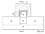
- FIGS. 6A and 6B illustrate the formation of gate dielectric 32 , gate electrode 34 , and gate spacers 36 .
- gate dielectric 32 is formed on the sidewalls and the top surface of fin 30 .
- the material of gate dielectric 32 may include silicon oxide, silicon nitride, or high-k dielectric materials such as Hf-containing dielectrics or any other kind of high-k materials, and the like.
- Gate electrode 34 may be formed of polysilicon, metals, metal silicides, and the like.
- FIG. 6B is a cross-sectional view of the structure shown in FIG. 6A , wherein the cross-sectional view is obtained from the vertical plane crossing line 6 B- 6 B in FIG. 6A .
- Gate spacers 36 are formed on the sidewalls of gate dielectric 32 and gate electrode 34 .
- dotted lines are used to illustrate the portions of gate dielectric 32 and gate electrode 34 that are on the sidewalls of fin 30 , since these portions of gate dielectric 32 and gate electrode 34 are not in the plane that is indicated as 6 B- 6 B in FIG. 6A .
- the bottom level of fin 30 is marked as 30 A.
- recesses 40 are formed, for example, by etching into silicon-containing layer 28 .
- recesses 40 extend into silicon-containing layer 28 , and do not extend into SiGe layer 26 .
- recesses extend down into SiGe layer 26 .
- Depth D 2 of recesses 40 may be between about one time to two times fin height H of fin 30 .
- the edges of recesses 40 may be substantially vertically aligned to the outer edges of gate spacers 36 . In other embodiments, recesses 40 may extend down to directly underlying gate spacers 36 .
- Dashed lines 42 illustrate the positions of the sidewalls and bottoms of recesses 40 in accordance with alternative embodiments.
- FIG. 8 illustrates the epitaxial growth of source/drain stressors 44 , which may also be formed through SEG.
- an n-type impurity such as phosphorous, arsenic, or combinations thereof, may be in-situ doped with the proceeding of the epitaxial growth of source/drain stressors 44 .
- the resulting n-type impurity concentration in source/drain stressors 44 may be between about 10 19 /cm 3 and about 10 22 /cm 3 .
- the material of source/drain stressors 44 may be expressed as Si 1 ⁇ y Ge y , wherein value y represents the atomic percentage of germanium, and is between (and may be equal to) 0 and 1.
- source/drain stressors 44 are silicon regions that have substantially no germanium added.
- Germanium percentage y in source/drain stressors 44 may be smaller than germanium atomic percentage x in SiGe layer 26 , and may be smaller than germanium atomic percentage z in silicon-containing layer 28 when silicon-containing layer 28 comprises silicon germanium.
- a difference between germanium atomic percentages x and y is greater than about 0.
- FIG. 9 illustrates the formation of remaining portions of NMOS FinFET 100 , which components include silicide regions 46 , contact plugs 48 , contact etch stop layer 50 , and inter-layer dielectric (ILD) 52 .
- source/drain stressors 44 may extend into SiGe layer 26 , or alternatively, not extend into SiGe layer 26 .
- source/drain stressors 44 may extend down to lower than bottom level 30 A of fin 30 , or have bottom surfaces substantially level with bottom level 30 A of fin 30 .
- FIG. 10 illustrates planar NMOS FET 200 in accordance with alternative embodiments. Unless specified otherwise, the reference numerals in these embodiments represent like elements in the embodiments illustrated in FIGS. 1 through 9 .
- the materials, dimensions, and the process steps for forming SiGe layer 26 , silicon-containing layer 28 , and source/drain stressors 44 may be essentially the same as the formation of the respective components in NMOS FinFET 100 .
- the formation process may include forming STI regions 22 in substrate 20 .
- a recess similar to recess 24 in FIG. 2 is then formed in substrate 20 , followed by the epitaxial growth of SiGe layer 26 and silicon-containing layer 28 .
- SiGe layer 26 is relaxed, so that its lattice constant is greater than the lattice constant of silicon.
- Silicon-containing layer 28 is un-relaxed, (either fully or partially), and its lattice constant is greater than the lattice constant of crystalline silicon, and may be substantially equal to the lattice constant of SiGe layer 26 . Accordingly, a tensile stress is generated in silicon-containing layer 28 .
- the step as shown in FIGS. 5A and 5B which step is for forming a fin, is skipped.
- gate dielectric 32 , gate electrode 34 , and source/drain stressors 44 are formed using essentially the same methods as for forming the corresponding components in NMOS FinFET 100 .
- source/drain stressors 44 are epitaxially grown from the un-relaxed silicon-containing layer 28 , which has the lattice constant substantially equal to the lattice constant of SiGe layer 26 .
- the germanium percentage of source/drain stressors 44 is lower than the germanium percentage of SiGe layer 26 . Accordingly, source/drain stressors 44 has a lattice constant smaller than the lattice constant of SiGe layer 26 , and smaller than the lattice constant of the un-relaxed silicon-containing layer 28 .
- source/drain stressors 44 results in a further increase in the tensile stress of the channel region of NMOS FinFET 100 ( FIG. 9 ) or planar NMOS FET 200 ( FIG. 10 ).
- the tensile stresses in the channel regions of the resulting NMOS FinFET 100 and planar NMOS FET 200 are thus greater than the respective NMOS FinFET and planar NMOS FET whose source/drain regions are formed by implanting n-type impurities, rather than by the epitaxial growth.
- source/drain stressors 44 makes the in-situ doping of phosphorous or arsenic possible.
- the in-situ doping of phosphorous or arsenic results in abrupt source/drain junctions, shallow source/drain junctions, and improved short channel effect.
- the concentrations of in-situ doped n-type impurities are higher than that in the source/drain regions that are formed through implantations. As a result of the increased impurity concentrations, the resistivities of the source/drain regions are reduced.
- a method of forming an NMOS FET includes forming a silicon germanium layer, and forming a silicon layer over the silicon germanium layer.
- a gate stack is formed over the silicon layer.
- the silicon layer is recessed to form a recess adjacent the gate stack.
- a silicon-containing semiconductor region is epitaxially grown in the recess to form a source/drain stressor, wherein the silicon-containing semiconductor region forms a source/drain region the NMOS FET.
- a method includes epitaxially growing a silicon germanium layer over a portion of a silicon substrate, and epitaxially growing a silicon layer over the silicon germanium layer.
- the silicon germanium layer is relaxed, and the silicon layer is un-relaxed.
- a gate stack is formed over the silicon layer, wherein a portion of the silicon layer forms a channel region of an NMOS FET.
- the silicon layer is then recessed to form recesses on opposite sides of the gate stack.
- Silicon germanium stressors are epitaxially grown in the recesses.
- the silicon germanium stressors have a germanium atomic percent lower than a germanium atomic percent of the silicon germanium layer.
- the silicon germanium stressors form source and drain regions of the NMOS FET.
- an NMOS FET includes a silicon germanium layer over a silicon substrate, wherein the silicon germanium layer is relaxed, either partially or fully.
- a silicon-containing layer is located over the silicon germanium layer, wherein the silicon-containing layer is at least partially un-relaxed, and wherein the germanium atomic percentage of the silicon-containing layer has a lower atomic percentage than in the silicon germanium layer.
- a gate stack is located over the silicon-containing layer, wherein a portion of the silicon-containing layer forms a channel region of the NMOS FET.
- Silicon-containing stressors are formed in the recesses in the silicon layer. The silicon-containing stressors have a lattice constant smaller than a lattice constant of the silicon germanium layer.
Landscapes
- Insulated Gate Type Field-Effect Transistor (AREA)
Abstract
A method of forming an n-type metal-oxide-semiconductor (NMOS) field-effect transistor (FET) includes forming a silicon germanium layer, and forming a silicon layer over the silicon germanium layer. A gate stack is formed over the silicon layer. The silicon layer is recessed to form a recess adjacent the gate stack. A silicon-containing semiconductor region is epitaxially grown in the recess to form a source/drain stressor, wherein the silicon-containing semiconductor region forms a source/drain region the NMOS FET.
Description
Inducing tensile stresses in the channels of n-type metal-oxide-semiconductor (NMOS) field-effect transistors (FETs) help improve the electron mobility in the channel regions. Inducing compressive stresses in the channels of p-type metal-oxide-semiconductor (PMOS) FETs help improve the hole mobility in the channel regions. With the improved carrier mobility, the drive currents of the NMOS FETs and PMOS FETs may be improved. There were various methods and structures for increasing the stresses in the NMOS and PMOS FETs, and new methods and structures are still being explored to further increase the stresses.
For a more complete understanding of the embodiments, and the advantages thereof, reference is now made to the following descriptions taken in conjunction with the accompanying drawings, in which:
The making and using of the embodiments of the disclosure are discussed in detail below. It should be appreciated, however, that the embodiments provide many applicable inventive concepts that can be embodied in a wide variety of specific contexts. The specific embodiments discussed are merely illustrative, and do not limit the scope of the disclosure.
An n-type metal-oxide-semiconductor (NMOS) field-effect transistor (FET) and the method of forming the same are provided in accordance with embodiments. The intermediate stages of manufacturing various embodiments are illustrated. The variations of the embodiments are discussed. Throughout the various views and illustrative embodiments, like reference numbers are used to designate like elements.
Referring to FIG. 1 , substrate 20, which may be a portion of a semiconductor wafer, is provided. Substrate 20 may be a semiconductor substrate. In an embodiment, substrate 20 is a silicon substrate with no germanium therein, although it may also be formed of silicon germanium (SiGe). Insulators such as shallow trench isolation (STI) regions 22 are formed in substrate 20. Depth D1 of STI regions 22 may be between about 50 nm and about 300 nm, or between about 100 nm and about 400 nm. It is realized, however, that the dimensions recited throughout the description are merely examples, and may be changed to different values. STI regions 22 may be formed by recessing semiconductor substrate 20 to form openings, and then filling the openings with dielectric materials. STI regions 22 may include two neighboring regions having their sidewalls facing each other, with a portion of substrate 20 between, and adjoining, the two neighboring STI regions 22.
Referring to FIG. 2 , the portion of substrate 20 that is between two neighboring STI regions 22 is removed, forming opening 24. In an embodiment, the bottom of opening 24 is level with the bottoms of STI regions 22. In alternative embodiments, the bottom of opening 24 may be lower than or higher than the bottoms of STI regions 22.
In FIG. 4 , silicon-containing layer 28 is epitaxially grown on SiGe layer 26. Silicon-containing layer 28 may have substantially pure silicon with substantially no germanium added, or alternatively, formed of silicon germanium that is expressed as Si1−zGez, wherein z is the atomic percentage of germanium in silicon-containing layer 28, and atomic percentage z may be equal to or greater than 0, and equal to or less than 1. Furthermore, atomic percentage z may be smaller than atomic percentage x of SiGe layer 26. With the proceeding of the epitaxial growth of silicon-containing layer 28, a p-type impurity such as boron and/or indium may be in-situ added to a low impurity concentration. Alternatively, the p-type impurity may be doped by implantation. The top surface of silicon-containing layer 28 may be substantially level with, or lower than, top surfaces of STI regions 22. Silicon-containing layer 28 has thickness T2, which may be between about 10 nm and about 100 nm. Thickness T2 is also small enough so that silicon-containing layer 28 is un-relaxed, either fully or partially, un-relaxed. For example, thickness T2 may be smaller than thickness T1. When silicon-containing layer 28 is un-relaxed, at least partially, the lattice constant of silicon-containing layer 28 is greater than the lattice constant of crystalline silicon, which is 5.43 Å, and may be equal to or substantially equal to (when silicon-containing layer 28 is fully un-relaxed) the lattice constant of SiGe layer 26, or smaller than (when silicon-containing layer 28 is partially un-relaxed) the lattice constant of SiGe layer 26. Accordingly, a tensile stress is generated in silicon-containing layer 28.
Referring to FIG. 5A , STI regions 22 are recessed, so that top surface 28A of silicon-containing layer 28 is higher than top surfaces 22A of the remaining portions of STI regions 22. In an embodiment, top surfaces 22A may be at an intermediate level that is between top surface 28A and bottom surface 28B of silicon-containing layer 28. In alternative embodiments, top surfaces 22A may be level with, or lower than, bottom surface 28B. Throughout the description, the portion of silicon-containing layer 28 (and possibly SiGe layer 26) that are over top surfaces 22A is referred to as fin 30. Fin 30 has fin height H. In an exemplary embodiment, fin height H is between about 10 nm and about 50 nm. FIG. 5B illustrates a cross-sectional view of the structure shown in FIG. 5A , wherein the cross-sectional view is obtained from the vertical plane crossing line 5B-5B in FIG. 5A .
Referring to FIG. 7 , which is a cross-sectional view obtained from the same plane as in FIG. 6B , recesses 40 are formed, for example, by etching into silicon-containing layer 28. In an embodiment, recesses 40 extend into silicon-containing layer 28, and do not extend into SiGe layer 26. In alternative embodiments, recesses extend down into SiGe layer 26. Depth D2 of recesses 40 may be between about one time to two times fin height H of fin 30. The edges of recesses 40 may be substantially vertically aligned to the outer edges of gate spacers 36. In other embodiments, recesses 40 may extend down to directly underlying gate spacers 36. Dashed lines 42 illustrate the positions of the sidewalls and bottoms of recesses 40 in accordance with alternative embodiments.
In the embodiments, source/drain stressors 44 are epitaxially grown from the un-relaxed silicon-containing layer 28, which has the lattice constant substantially equal to the lattice constant of SiGe layer 26. In addition, the germanium percentage of source/drain stressors 44 is lower than the germanium percentage of SiGe layer 26. Accordingly, source/drain stressors 44 has a lattice constant smaller than the lattice constant of SiGe layer 26, and smaller than the lattice constant of the un-relaxed silicon-containing layer 28. As a result, the formation of source/drain stressors 44 results in a further increase in the tensile stress of the channel region of NMOS FinFET 100 (FIG. 9 ) or planar NMOS FET 200 (FIG. 10 ). The tensile stresses in the channel regions of the resulting NMOS FinFET 100 and planar NMOS FET 200 are thus greater than the respective NMOS FinFET and planar NMOS FET whose source/drain regions are formed by implanting n-type impurities, rather than by the epitaxial growth.
In addition, the epitaxial growth of source/drain stressors 44 (FIG. 8 ) makes the in-situ doping of phosphorous or arsenic possible. The in-situ doping of phosphorous or arsenic results in abrupt source/drain junctions, shallow source/drain junctions, and improved short channel effect. Furthermore, the concentrations of in-situ doped n-type impurities are higher than that in the source/drain regions that are formed through implantations. As a result of the increased impurity concentrations, the resistivities of the source/drain regions are reduced.
In accordance with embodiments, a method of forming an NMOS FET includes forming a silicon germanium layer, and forming a silicon layer over the silicon germanium layer. A gate stack is formed over the silicon layer. The silicon layer is recessed to form a recess adjacent the gate stack. A silicon-containing semiconductor region is epitaxially grown in the recess to form a source/drain stressor, wherein the silicon-containing semiconductor region forms a source/drain region the NMOS FET.
In accordance with other embodiments, a method includes epitaxially growing a silicon germanium layer over a portion of a silicon substrate, and epitaxially growing a silicon layer over the silicon germanium layer. The silicon germanium layer is relaxed, and the silicon layer is un-relaxed. A gate stack is formed over the silicon layer, wherein a portion of the silicon layer forms a channel region of an NMOS FET. The silicon layer is then recessed to form recesses on opposite sides of the gate stack. Silicon germanium stressors are epitaxially grown in the recesses. The silicon germanium stressors have a germanium atomic percent lower than a germanium atomic percent of the silicon germanium layer. The silicon germanium stressors form source and drain regions of the NMOS FET.
In accordance with yet other embodiments, an NMOS FET includes a silicon germanium layer over a silicon substrate, wherein the silicon germanium layer is relaxed, either partially or fully. A silicon-containing layer is located over the silicon germanium layer, wherein the silicon-containing layer is at least partially un-relaxed, and wherein the germanium atomic percentage of the silicon-containing layer has a lower atomic percentage than in the silicon germanium layer. A gate stack is located over the silicon-containing layer, wherein a portion of the silicon-containing layer forms a channel region of the NMOS FET. Silicon-containing stressors are formed in the recesses in the silicon layer. The silicon-containing stressors have a lattice constant smaller than a lattice constant of the silicon germanium layer.
Although the embodiments and their advantages have been described in detail, it should be understood that various changes, substitutions and alterations can be made herein without departing from the spirit and scope of the embodiments as defined by the appended claims. Moreover, the scope of the present application is not intended to be limited to the particular embodiments of the process, machine, manufacture, and composition of matter, means, methods and steps described in the specification. As one of ordinary skill in the art will readily appreciate from the disclosure, processes, machines, manufacture, compositions of matter, means, methods, or steps, presently existing or later to be developed, that perform substantially the same function or achieve substantially the same result as the corresponding embodiments described herein may be utilized according to the disclosure. Accordingly, the appended claims are intended to include within their scope such processes, machines, manufacture, compositions of matter, means, methods, or steps. In addition, each claim constitutes a separate embodiment, and the combination of various claims and embodiments are within the scope of the disclosure.
Claims (13)
1. A method comprising:
forming a silicon germanium layer;
forming a silicon-containing layer over the silicon germanium layer, wherein an atomic percentage of the silicon-containing layer is lower than an atomic percentage of the silicon germanium layer;
forming a gate stack over the silicon-containing layer and the silicon germanium layer;
recessing the silicon-containing layer to form a recess adjacent the gate stack; and
epitaxially growing a silicon-containing semiconductor region in the recess to form a source/drain stressor, wherein the silicon-containing semiconductor region forms a source/drain region of an n-type metal-oxide-semiconductor (NMOS) field-effect transistor (FET).
2. The method of claim 1 , wherein the silicon germanium layer is relaxed, and the silicon-containing layer is fully un-relaxed, wherein a lattice constant of the silicon-containing layer is greater than 5.43 Å, and is equal to a lattice constant of the silicon germanium layer.
3. The method of claim 1 , wherein the silicon germanium layer is relaxed, and the silicon-containing layer is partially un-relaxed, wherein a lattice constant of the silicon-containing layer is greater than 5.43 Å, and is smaller than a lattice constant of the silicon germanium layer.
4. The method of claim 1 , wherein the silicon germanium layer is fully relaxed.
5. The method of claim 1 , wherein the step of epitaxially growing the silicon-containing semiconductor region comprises epitaxially growing a silicon germanium stressor, and wherein the silicon germanium stressor has a germanium atomic percentage lower than a germanium atomic percentage of the silicon germanium layer.
6. The method of claim 1 , wherein the step of epitaxially growing the silicon-containing semiconductor region comprises epitaxially growing a silicon stressor, and wherein the silicon stressor is free from germanium.
7. The method of claim 1 further comprising in-situ doping an n-type impurity simultaneously with the step of epitaxially growing the silicon-containing semiconductor region.
8. The method of claim 1 , wherein the atomic percentage of the silicon-containing layer is equal to zero.
9. A method comprising:
epitaxially growing a silicon germanium layer over a portion of a silicon substrate;
epitaxially growing a silicon layer over the silicon germanium layer, wherein the silicon germanium layer is relaxed, and the silicon layer is un-relaxed;
forming a gate stack over the silicon layer and the silicon germanium layer, wherein a portion of the silicon layer forms a channel region of an n-type metal-oxide-semiconductor (NMOS) field-effect transistor (FET);
recessing the silicon layer to form recesses on opposite sides of the gate stack; and
epitaxially growing silicon germanium stressors in the recesses, wherein the silicon germanium stressors have a germanium atomic percent lower than a germanium atomic percent of the silicon germanium layer, and wherein the silicon germanium stressors form source and drain regions of the NMOS FET.
10. The method of claim 9 further comprising in-situ doping an n-type impurity in the silicon germanium stressors, wherein the step of in-situ doping is performed simultaneously with the step of epitaxially growing the silicon germanium stressors.
11. The method of claim 9 , wherein during the step of recessing, top portions of the silicon germanium layer is recessed along with portions of the silicon layer.
12. The method of claim 9 , wherein the silicon germanium stressors do not extend into the silicon germanium layer.
13. The method of claim 9 , wherein the silicon germanium stressors extends into the silicon germanium layer.
Priority Applications (2)
| Application Number | Priority Date | Filing Date | Title |
|---|---|---|---|
| US13/189,119 US8609518B2 (en) | 2011-07-22 | 2011-07-22 | Re-growing source/drain regions from un-relaxed silicon layer |
| US14/078,141 US9508849B2 (en) | 2011-07-22 | 2013-11-12 | Device having source/drain regions regrown from un-relaxed silicon layer |
Applications Claiming Priority (1)
| Application Number | Priority Date | Filing Date | Title |
|---|---|---|---|
| US13/189,119 US8609518B2 (en) | 2011-07-22 | 2011-07-22 | Re-growing source/drain regions from un-relaxed silicon layer |
Related Child Applications (1)
| Application Number | Title | Priority Date | Filing Date |
|---|---|---|---|
| US14/078,141 Division US9508849B2 (en) | 2011-07-22 | 2013-11-12 | Device having source/drain regions regrown from un-relaxed silicon layer |
Publications (2)
| Publication Number | Publication Date |
|---|---|
| US20130020612A1 US20130020612A1 (en) | 2013-01-24 |
| US8609518B2 true US8609518B2 (en) | 2013-12-17 |
Family
ID=47555188
Family Applications (2)
| Application Number | Title | Priority Date | Filing Date |
|---|---|---|---|
| US13/189,119 Active 2031-12-14 US8609518B2 (en) | 2011-07-22 | 2011-07-22 | Re-growing source/drain regions from un-relaxed silicon layer |
| US14/078,141 Expired - Fee Related US9508849B2 (en) | 2011-07-22 | 2013-11-12 | Device having source/drain regions regrown from un-relaxed silicon layer |
Family Applications After (1)
| Application Number | Title | Priority Date | Filing Date |
|---|---|---|---|
| US14/078,141 Expired - Fee Related US9508849B2 (en) | 2011-07-22 | 2013-11-12 | Device having source/drain regions regrown from un-relaxed silicon layer |
Country Status (1)
| Country | Link |
|---|---|
| US (2) | US8609518B2 (en) |
Cited By (79)
| Publication number | Priority date | Publication date | Assignee | Title |
|---|---|---|---|---|
| US20160190318A1 (en) * | 2014-12-30 | 2016-06-30 | Taiwan Semiconductor Manufacturing Co., Ltd. | Semiconductor device and manufacturing method thereof |
| US9391201B2 (en) | 2014-11-25 | 2016-07-12 | Taiwan Semiconductor Manufacturing Company, Ltd. | Source/drain structure and manufacturing the same |
| US9425313B1 (en) | 2015-07-07 | 2016-08-23 | Taiwan Semiconductor Manufacturing Co., Ltd. | Semiconductor device and manufacturing method thereof |
| US9425250B2 (en) | 2014-12-30 | 2016-08-23 | Taiwan Semiconductor Manufacturing Company, Ltd. | Transistor with wurtzite channel |
| US20160254351A1 (en) * | 2015-02-26 | 2016-09-01 | Taiwan Semiconductor Manufacturing Company Ltd. | Ldd-free semiconductor structure and manufacturing method of the same |
| US9443729B1 (en) | 2015-03-31 | 2016-09-13 | Taiwan Semiconductor Manufacturing Company, Ltd. | Method for forming FinFET devices |
| US9449975B1 (en) | 2015-06-15 | 2016-09-20 | Taiwan Semiconductor Manufacturing Company, Ltd. | FinFET devices and methods of forming |
| US9461110B1 (en) | 2015-04-30 | 2016-10-04 | Taiwan Semiconductor Manufacturing Company, Ltd. | FETs and methods of forming FETs |
| US9472620B1 (en) | 2015-09-04 | 2016-10-18 | Taiwan Semiconductor Manufacturing Co., Ltd. | Semiconductor device including fin structures and manufacturing method thereof |
| US9515071B2 (en) | 2014-12-24 | 2016-12-06 | Taiwan Semiconductor Manufacturing Company, Ltd. | Asymmetric source/drain depths |
| US9564317B1 (en) | 2015-12-02 | 2017-02-07 | Taiwan Semiconductor Manufacturing Company, Ltd. | Method of forming a nanowire |
| US9570557B2 (en) | 2015-04-29 | 2017-02-14 | Taiwan Semiconductor Manufacturing Co., Ltd. | Tilt implantation for STI formation in FinFET structures |
| US9590102B2 (en) | 2015-04-15 | 2017-03-07 | Taiwan Semiconductor Manufacturing Co., Ltd. | Semiconductor device and manufacturing method thereof |
| US9601626B2 (en) | 2015-01-23 | 2017-03-21 | Taiwan Semiconductor Manufacturing Co., Ltd. | Semiconductor device including fin structure with two channel layers and manufacturing method thereof |
| US9620628B1 (en) | 2016-07-07 | 2017-04-11 | Taiwan Semiconductor Manufacturing Co., Ltd. | Methods of forming contact feature |
| US9647090B2 (en) | 2014-12-30 | 2017-05-09 | Taiwan Semiconductor Manufacturing Company, Ltd. | Surface passivation for germanium-based semiconductor structure |
| US9647071B2 (en) | 2015-06-15 | 2017-05-09 | Taiwan Semiconductor Manufacturing Company, Ltd. | FINFET structures and methods of forming the same |
| US9660033B1 (en) | 2016-01-13 | 2017-05-23 | Taiwan Semiconductor Manufactuing Company, Ltd. | Multi-gate device and method of fabrication thereof |
| US9680014B2 (en) | 2015-04-17 | 2017-06-13 | Taiwan Semiconductor Manufacturing Co., Ltd. | Semiconductor device including Fin structures and manufacturing method thereof |
| US9680017B2 (en) | 2015-09-16 | 2017-06-13 | Taiwan Semiconductor Manufacturing Co., Ltd. | Semiconductor device including Fin FET and manufacturing method thereof |
| US9716146B2 (en) | 2015-12-15 | 2017-07-25 | Taiwan Semiconductor Manufacturing Company, Ltd. | Integrated circuit structure and method with solid phase diffusion |
| US9728461B2 (en) | 2014-12-12 | 2017-08-08 | Taiwan Semiconductor Manufacturing Company, Ltd. | Method of forming semiconductor device with different threshold voltages |
| US9768301B2 (en) | 2014-12-23 | 2017-09-19 | Taiwan Semiconductor Manufacturing Company, Ltd. | Short channel effect suppression |
| US9773786B2 (en) | 2015-04-30 | 2017-09-26 | Taiwan Semiconductor Manufacturing Company, Ltd. | FETs and methods of forming FETs |
| US9780214B2 (en) | 2014-12-22 | 2017-10-03 | Taiwan Semiconductor Manufacturing Co., Ltd. | Semiconductor device including Fin- FET and manufacturing method thereof |
| US9847334B1 (en) | 2016-11-18 | 2017-12-19 | Taiwan Semiconductor Manufacturing Co., Ltd. | Structure and formation method of semiconductor device with channel layer |
| US9853150B1 (en) | 2016-08-15 | 2017-12-26 | Taiwan Semiconductor Manufacturing Co., Ltd. | Method of fabricating epitaxial gate dielectrics and semiconductor device of the same |
| US9865595B1 (en) | 2016-12-14 | 2018-01-09 | Taiwan Semiconductor Manufacturing Co., Ltd. | FinFET device with epitaxial structures that wrap around the fins and the method of fabricating the same |
| US9865589B1 (en) | 2016-10-31 | 2018-01-09 | Taiwan Semiconductor Manufacturing Co., Ltd. | System and method of fabricating ESD FinFET with improved metal landing in the drain |
| US9876098B2 (en) | 2016-01-15 | 2018-01-23 | Taiwan Semiconductor Manufacturing Company, Ltd. | Method of forming a gate spacer |
| US9887269B2 (en) | 2015-11-30 | 2018-02-06 | Taiwan Semiconductor Manufacturing Company, Ltd. | Multi-gate device and method of fabrication thereof |
| US9899273B1 (en) | 2016-12-15 | 2018-02-20 | Taiwan Semiconductor Manufacturing Co., Ltd. | Semiconductor structure with dopants diffuse protection and method for forming the same |
| US9899269B2 (en) | 2015-12-30 | 2018-02-20 | Taiwan Semiconductor Manufacturing Company, Ltd | Multi-gate device and method of fabrication thereof |
| US9953881B2 (en) | 2015-07-20 | 2018-04-24 | Taiwan Semiconductor Manufacturing Company, Ltd. | Method of forming a FinFET device |
| US9960273B2 (en) | 2015-11-16 | 2018-05-01 | Taiwan Semiconductor Manufacturing Company, Ltd. | Integrated circuit structure with substrate isolation and un-doped channel |
| US10008414B2 (en) | 2016-06-28 | 2018-06-26 | Taiwan Semiconductor Manufacturing Co., Ltd. | System and method for widening Fin widths for small pitch FinFET devices |
| US10032627B2 (en) | 2015-11-16 | 2018-07-24 | Taiwan Semiconductor Manufacturing Company, Ltd. | Method for forming stacked nanowire transistors |
| US10038095B2 (en) | 2016-01-28 | 2018-07-31 | Taiwan Semiconductor Manufacturing Co., Ltd. | V-shape recess profile for embedded source/drain epitaxy |
| US10062782B2 (en) | 2016-11-29 | 2018-08-28 | Taiwan Semiconductor Manufacturing Co., Ltd. | Method of manufacturing a semiconductor device with multilayered channel structure |
| US10115826B2 (en) | 2013-09-13 | 2018-10-30 | Taiwan Semiconductor Manufacturing Company Ltd. | Semiconductor structure and the manufacturing method thereof |
| US10121858B2 (en) | 2015-10-30 | 2018-11-06 | Taiwan Semiconductor Manufacturing Company, Ltd. | Elongated semiconductor structure planarization |
| US10134871B2 (en) | 2014-12-23 | 2018-11-20 | Taiwan Semiconductor Manufacturing Company, Ltd. | Doping of high-K dielectric oxide by wet chemical treatment |
| US10134870B2 (en) | 2016-11-28 | 2018-11-20 | Taiwan Semiconductor Manufacturing Co., Ltd. | Semiconductor structure and method of manufacturing the same |
| US10141310B2 (en) | 2014-12-23 | 2018-11-27 | Taiwan Semiconductor Manufacturing Company, Ltd. | Short channel effect suppression |
| US10164061B2 (en) | 2016-05-19 | 2018-12-25 | Taiwan Semiconductor Manufacturing Co., Ltd. | Method of fabricating non-volatile memory device array |
| US10170375B2 (en) | 2014-03-13 | 2019-01-01 | Taiwan Semiconductor Manufacturing Company, Ltd. | FinFET devices with unique fin shape and the fabrication thereof |
| US10217741B2 (en) | 2016-08-03 | 2019-02-26 | Taiwan Semiconductor Manufacturing Company, Ltd. | Fin structure and method of forming same through two-step etching processes |
| US10269938B2 (en) | 2016-07-15 | 2019-04-23 | Taiwan Semiconductor Manufacturing Co., Ltd. | Semiconductor device structure having a doped passivation layer |
| US10269968B2 (en) | 2015-06-03 | 2019-04-23 | Taiwan Semiconductor Manufacturing Co., Ltd. | Semiconductor device including fin structures and manufacturing method thereof |
| US10276697B1 (en) | 2017-10-27 | 2019-04-30 | Taiwan Semiconductor Manufacturing Co., Ltd. | Negative capacitance FET with improved reliability performance |
| US10290546B2 (en) | 2016-11-29 | 2019-05-14 | Taiwan Semiconductor Manufacturing Co., Ltd. | Threshold voltage adjustment for a gate-all-around semiconductor structure |
| US10340383B2 (en) | 2016-03-25 | 2019-07-02 | Taiwan Semiconductor Manufacturing Co., Ltd. | Semiconductor device having stressor layer |
| US10366915B2 (en) | 2017-11-15 | 2019-07-30 | Taiwan Semiconductor Manufacturing Co., Ltd. | FinFET devices with embedded air gaps and the fabrication thereof |
| US10388771B1 (en) | 2018-06-28 | 2019-08-20 | Taiwan Semiconductor Manufacturing Co., Ltd. | Method and device for forming cut-metal-gate feature |
| US10453925B2 (en) | 2016-01-29 | 2019-10-22 | Taiwan Semiconductor Manufacturing Co., Ltd. | Epitaxial growth methods and structures thereof |
| US10453753B2 (en) | 2017-08-31 | 2019-10-22 | Taiwan Semiconductor Manufacturing Co., Ltd. | Using a metal-containing layer as an etching stop layer and to pattern source/drain regions of a FinFET |
| US10510894B2 (en) | 2017-11-30 | 2019-12-17 | Taiwan Semiconductor Manufacturing Co., Ltd. | Isolation structure having different distances to adjacent FinFET devices |
| US10522417B2 (en) | 2017-04-27 | 2019-12-31 | Taiwan Semiconductor Manufacturing Co., Ltd. | FinFET device with different liners for PFET and NFET and method of fabricating thereof |
| US10522557B2 (en) | 2017-10-30 | 2019-12-31 | Taiwan Semiconductor Manufacturing Co., Ltd. | Surface topography by forming spacer-like components |
| US10522643B2 (en) | 2017-04-26 | 2019-12-31 | Taiwan Semiconductor Manufacturing Co., Ltd. | Device and method for tuning threshold voltage by implementing different work function metals in different segments of a gate |
| US10529831B1 (en) | 2018-08-03 | 2020-01-07 | Globalfoundries Inc. | Methods, apparatus, and system for forming epitaxial formations with reduced risk of merging |
| US20200144374A1 (en) * | 2017-06-30 | 2020-05-07 | Intel Corporation | Transistor with wide bandgap channel and narrow bandgap source/drain |
| US10665697B2 (en) | 2018-06-15 | 2020-05-26 | Taiwan Semiconductor Manufacturing Company, Ltd. | Semiconductor device and method |
| US10734522B2 (en) | 2016-06-15 | 2020-08-04 | Taiwan Semiconductor Manufacturing Co., Ltd. | Structure and formation method of semiconductor device structure with gate stacks |
| US10790352B2 (en) | 2018-06-28 | 2020-09-29 | Taiwan Semiconductor Manufacturing Co., Ltd. | High density capacitor implemented using FinFET |
| US10854615B2 (en) | 2018-03-30 | 2020-12-01 | Taiwan Semiconductor Manufacturing Co., Ltd. | FinFET having non-merging epitaxially grown source/drains |
| US10879240B2 (en) | 2016-11-18 | 2020-12-29 | Taiwan Semiconductor Manufacturing Co., Ltd. | Fin field effect transistor (FinFET) device structure |
| US10886226B2 (en) | 2018-07-31 | 2021-01-05 | Taiwan Semiconductor Manufacturing Co, Ltd. | Conductive contact having staircase barrier layers |
| US10971605B2 (en) | 2018-10-22 | 2021-04-06 | Taiwan Semiconductor Manufacturing Co., Ltd. | Dummy dielectric fin design for parasitic capacitance reduction |
| US10998241B2 (en) | 2018-09-19 | 2021-05-04 | Taiwan Semiconductor Manufacturing Co., Ltd. | Selective dual silicide formation using a maskless fabrication process flow |
| US11011634B2 (en) | 2016-11-30 | 2021-05-18 | Taiwan Semiconductor Manufacturing Co., Ltd. | Elongated source/drain region structure in finFET device |
| US11152362B2 (en) | 2016-11-10 | 2021-10-19 | Taiwan Semiconductor Manufacturing Co., Ltd. | Fin field effect transistor (FinFET) device structure |
| US11302535B2 (en) | 2018-06-27 | 2022-04-12 | Taiwan Semiconductor Manufacturing Co., Ltd. | Performing annealing process to improve fin quality of a FinFET semiconductor |
| US11469238B2 (en) | 2019-09-26 | 2022-10-11 | Taiwan Semiconductor Manufacturing Co., Ltd. | Non-interleaving N-well and P-well pickup region design for IC devices |
| US11728344B2 (en) | 2019-06-28 | 2023-08-15 | Taiwan Semiconductor Manufacturing Co., Ltd. | Hybrid SRAM design with nano-structures |
| US12046479B2 (en) | 2020-08-13 | 2024-07-23 | Taiwan Semiconductor Manufacturing Company, Ltd. | Nitride-containing STI liner for SiGe channel |
| US12165869B2 (en) | 2015-11-16 | 2024-12-10 | Taiwan Semiconductor Manufacturing Co., Ltd. | Transistors comprising a vertical stack of elongated semiconductor features |
| US12266709B2 (en) | 2018-09-19 | 2025-04-01 | Taiwan Semiconductor Manufacturing Co., Ltd. | Selective dual silicide formation using a maskless fabrication process flow |
| US12369374B2 (en) | 2022-07-28 | 2025-07-22 | Taiwan Semicoductor Manufacturing Co., Ltd. | Epitaxial growth methods and structures thereof |
Families Citing this family (18)
| Publication number | Priority date | Publication date | Assignee | Title |
|---|---|---|---|---|
| KR101776926B1 (en) | 2010-09-07 | 2017-09-08 | 삼성전자주식회사 | Semiconductor device and method for manufacturing the same |
| US9847225B2 (en) * | 2011-11-15 | 2017-12-19 | Taiwan Semiconductor Manufacturing Company, Ltd. | Semiconductor device and method of manufacturing the same |
| US8659097B2 (en) * | 2012-01-16 | 2014-02-25 | Taiwan Semiconductor Manufacturing Company, Ltd. | Control fin heights in FinFET structures |
| US8716765B2 (en) | 2012-03-23 | 2014-05-06 | Taiwan Semiconductor Manufacturing Company, Ltd. | Contact structure of semiconductor device |
| US8779554B2 (en) * | 2012-03-30 | 2014-07-15 | Taiwan Semiconductor Manufacturing Company, Ltd. | MOSFETs with channels on nothing and methods for forming the same |
| US9209066B2 (en) * | 2013-03-01 | 2015-12-08 | Taiwan Semiconductor Manufacturing Company, Ltd. | Isolation structure of semiconductor device |
| CN104124172B (en) * | 2013-04-28 | 2017-07-14 | 中芯国际集成电路制造(上海)有限公司 | Fin formula field effect transistor and forming method thereof |
| US9246005B2 (en) | 2014-02-12 | 2016-01-26 | International Business Machines Corporation | Stressed channel bulk fin field effect transistor |
| US9276113B2 (en) * | 2014-03-10 | 2016-03-01 | International Business Corporation | Structure and method to make strained FinFET with improved junction capacitance and low leakage |
| US10553718B2 (en) * | 2014-03-14 | 2020-02-04 | Taiwan Semiconductor Manufacturing Co., Ltd. | Semiconductor devices with core-shell structures |
| US10243078B2 (en) | 2014-12-17 | 2019-03-26 | Intel Corporation | Carrier confinement for high mobility channel devices |
| TWI662699B (en) * | 2015-11-04 | 2019-06-11 | 聯華電子股份有限公司 | Semiconductor structure and manufacturing method thereof |
| US9768072B1 (en) | 2016-06-30 | 2017-09-19 | International Business Machines Corporation | Fabrication of a vertical fin field effect transistor with reduced dimensional variations |
| US10304957B2 (en) * | 2016-09-13 | 2019-05-28 | Qualcomm Incorporated | FinFET with reduced series total resistance |
| US10522359B2 (en) | 2016-11-29 | 2019-12-31 | Taiwan Semiconductor Manufacturing Company, Ltd. | FinFET device and method of forming |
| WO2018125191A1 (en) * | 2016-12-30 | 2018-07-05 | Intel Corporation | Subfin liner for finfet devices |
| CN111725208B (en) * | 2019-03-21 | 2023-09-19 | 中芯国际集成电路制造(上海)有限公司 | Semiconductor structure and method of forming same |
| US11935793B2 (en) * | 2020-05-29 | 2024-03-19 | Taiwan Semiconductor Manufacturing Co., Ltd. | Dual dopant source/drain regions and methods of forming same |
Citations (6)
| Publication number | Priority date | Publication date | Assignee | Title |
|---|---|---|---|---|
| US20060011984A1 (en) * | 2002-06-07 | 2006-01-19 | Amberwave Systems Corporation | Control of strain in device layers by selective relaxation |
| US20060030093A1 (en) * | 2004-08-06 | 2006-02-09 | Da Zhang | Strained semiconductor devices and method for forming at least a portion thereof |
| US20070057287A1 (en) * | 2005-09-15 | 2007-03-15 | Taiwan Semiconductor Manufacturing Company, Ltd. | Embedded SiGe stressor with tensile strain for NMOS current enhancement |
| US20070190730A1 (en) * | 2006-02-13 | 2007-08-16 | Taiwan Semiconductor Manufacturing Company, Ltd. | Resolving pattern-loading issues of SiGe stressor |
| US20070238250A1 (en) * | 2006-03-30 | 2007-10-11 | Freescale Semiconductor, Inc. | Semiconductor fabrication process using etch stop layer to optimize formation of source/drain stressor |
| US20110303980A1 (en) * | 2010-06-09 | 2011-12-15 | Globalfoundries Inc. | Semiconductor devices having stressor regions and related fabrication methods |
Family Cites Families (2)
| Publication number | Priority date | Publication date | Assignee | Title |
|---|---|---|---|---|
| US6830976B2 (en) * | 2001-03-02 | 2004-12-14 | Amberwave Systems Corproation | Relaxed silicon germanium platform for high speed CMOS electronics and high speed analog circuits |
| TWI242232B (en) * | 2003-06-09 | 2005-10-21 | Canon Kk | Semiconductor substrate, semiconductor device, and method of manufacturing the same |
-
2011
- 2011-07-22 US US13/189,119 patent/US8609518B2/en active Active
-
2013
- 2013-11-12 US US14/078,141 patent/US9508849B2/en not_active Expired - Fee Related
Patent Citations (6)
| Publication number | Priority date | Publication date | Assignee | Title |
|---|---|---|---|---|
| US20060011984A1 (en) * | 2002-06-07 | 2006-01-19 | Amberwave Systems Corporation | Control of strain in device layers by selective relaxation |
| US20060030093A1 (en) * | 2004-08-06 | 2006-02-09 | Da Zhang | Strained semiconductor devices and method for forming at least a portion thereof |
| US20070057287A1 (en) * | 2005-09-15 | 2007-03-15 | Taiwan Semiconductor Manufacturing Company, Ltd. | Embedded SiGe stressor with tensile strain for NMOS current enhancement |
| US20070190730A1 (en) * | 2006-02-13 | 2007-08-16 | Taiwan Semiconductor Manufacturing Company, Ltd. | Resolving pattern-loading issues of SiGe stressor |
| US20070238250A1 (en) * | 2006-03-30 | 2007-10-11 | Freescale Semiconductor, Inc. | Semiconductor fabrication process using etch stop layer to optimize formation of source/drain stressor |
| US20110303980A1 (en) * | 2010-06-09 | 2011-12-15 | Globalfoundries Inc. | Semiconductor devices having stressor regions and related fabrication methods |
Non-Patent Citations (4)
| Title |
|---|
| Chu, M., et al., "Comparison between high-field piezoresistance coefficients of Si metal-oxide-semiconductor field-effect transistors and bulk Si under uniaxial and biaxial stress," Journal of Applied Physics 103, 113704, 2008, 7 pgs. |
| Eguchi, S., et al., "Comparison of arsenic and phosphorus diffusion behavior in silicon-germanium alloys," Applied Physics Letters, vol. 80, No. 10, Mar. 11, 2002, pp. 1743-1745. |
| Jang, S.-M., et al., "Phosphorus doping of epitaxial Si and Si1-x Gexat very low pressure," Applied Physics Letters, vol. 63, No. 12, Sep. 20, 1993, pp. 1675-1677. |
| Schindler, M., et al., "Selective epitaxial growth of Arsenic-doped SiGe-structures with LPCVD," ECS Transactions, 1 (30), 2006, pp. 33-40. |
Cited By (171)
| Publication number | Priority date | Publication date | Assignee | Title |
|---|---|---|---|---|
| US10115826B2 (en) | 2013-09-13 | 2018-10-30 | Taiwan Semiconductor Manufacturing Company Ltd. | Semiconductor structure and the manufacturing method thereof |
| US10622261B2 (en) | 2014-03-13 | 2020-04-14 | Taiwan Semiconductor Manufacturing Co., Ltd. | FinFET devices with unique shape and the fabrication thereof |
| US10170375B2 (en) | 2014-03-13 | 2019-01-01 | Taiwan Semiconductor Manufacturing Company, Ltd. | FinFET devices with unique fin shape and the fabrication thereof |
| US10367094B2 (en) | 2014-11-25 | 2019-07-30 | Taiwan Semiconductor Manufacturing Company, Ltd. | Source/drain structure having multi-facet surfaces |
| US9391201B2 (en) | 2014-11-25 | 2016-07-12 | Taiwan Semiconductor Manufacturing Company, Ltd. | Source/drain structure and manufacturing the same |
| US10854749B2 (en) | 2014-11-25 | 2020-12-01 | Taiwan Semiconductor Manufacturing Company, Ltd. | Source/drain structure having multi-facet surfaces |
| US9876112B2 (en) | 2014-11-25 | 2018-01-23 | Taiwan Semiconductor Manufacturing Company, Ltd. | Source/drain structure and manufacturing the same |
| US11901452B2 (en) | 2014-11-25 | 2024-02-13 | Taiwan Semiconductor Manufacturing Company, Ltd. | Source/drain structure having multi-facet surface |
| US9728461B2 (en) | 2014-12-12 | 2017-08-08 | Taiwan Semiconductor Manufacturing Company, Ltd. | Method of forming semiconductor device with different threshold voltages |
| US9882029B2 (en) | 2014-12-22 | 2018-01-30 | Taiwan Semiconductor Manufacturing Co., Ltd. | Semiconductor device including Fin-FET and manufacturing method thereof |
| US9780214B2 (en) | 2014-12-22 | 2017-10-03 | Taiwan Semiconductor Manufacturing Co., Ltd. | Semiconductor device including Fin- FET and manufacturing method thereof |
| US10269935B2 (en) | 2014-12-22 | 2019-04-23 | Taiwan Semiconductor Manufacturing Co., Ltd. | Semiconductor device including Fin-PET and manufacturing method thereof |
| US10134871B2 (en) | 2014-12-23 | 2018-11-20 | Taiwan Semiconductor Manufacturing Company, Ltd. | Doping of high-K dielectric oxide by wet chemical treatment |
| US10141310B2 (en) | 2014-12-23 | 2018-11-27 | Taiwan Semiconductor Manufacturing Company, Ltd. | Short channel effect suppression |
| US9768301B2 (en) | 2014-12-23 | 2017-09-19 | Taiwan Semiconductor Manufacturing Company, Ltd. | Short channel effect suppression |
| US9515071B2 (en) | 2014-12-24 | 2016-12-06 | Taiwan Semiconductor Manufacturing Company, Ltd. | Asymmetric source/drain depths |
| US20160190318A1 (en) * | 2014-12-30 | 2016-06-30 | Taiwan Semiconductor Manufacturing Co., Ltd. | Semiconductor device and manufacturing method thereof |
| US9647090B2 (en) | 2014-12-30 | 2017-05-09 | Taiwan Semiconductor Manufacturing Company, Ltd. | Surface passivation for germanium-based semiconductor structure |
| US9679961B2 (en) | 2014-12-30 | 2017-06-13 | Taiwan Semiconductor Manufacturing Company, Ltd. | Transistor with wurtzite channel |
| US9425250B2 (en) | 2014-12-30 | 2016-08-23 | Taiwan Semiconductor Manufacturing Company, Ltd. | Transistor with wurtzite channel |
| US9601626B2 (en) | 2015-01-23 | 2017-03-21 | Taiwan Semiconductor Manufacturing Co., Ltd. | Semiconductor device including fin structure with two channel layers and manufacturing method thereof |
| US10326023B2 (en) | 2015-01-23 | 2019-06-18 | Taiwan Semiconductor Manufacturing Co., Ltd. | Semiconductor device including fin structure with two channel layers and manufacturing method thereof |
| US9966469B2 (en) | 2015-01-23 | 2018-05-08 | Taiwan Semiconductor Manufacturing Co., Ltd. | Semiconductor device including fin structure with two channel layers and manufacturing method thereof |
| CN105932060B (en) * | 2015-02-26 | 2019-08-09 | 台湾积体电路制造股份有限公司 | Semiconductor structure without lightly doped drain and method of manufacturing the same |
| US9991343B2 (en) * | 2015-02-26 | 2018-06-05 | Taiwan Semiconductor Manufacturing Company Ltd. | LDD-free semiconductor structure and manufacturing method of the same |
| CN105932060A (en) * | 2015-02-26 | 2016-09-07 | 台湾积体电路制造股份有限公司 | LDD-free semiconductor structure and manufacturing method of the same |
| US20160254351A1 (en) * | 2015-02-26 | 2016-09-01 | Taiwan Semiconductor Manufacturing Company Ltd. | Ldd-free semiconductor structure and manufacturing method of the same |
| US10269899B2 (en) | 2015-03-31 | 2019-04-23 | Taiwan Semiconductor Manufacturing Company, Ltd. | Method for forming FinFET devices |
| US9443729B1 (en) | 2015-03-31 | 2016-09-13 | Taiwan Semiconductor Manufacturing Company, Ltd. | Method for forming FinFET devices |
| US10644154B2 (en) | 2015-04-15 | 2020-05-05 | Taiwan Semiconductor Manufacturing Co., Ltd. | Semiconductor device and manufacturing method thereof |
| US9590102B2 (en) | 2015-04-15 | 2017-03-07 | Taiwan Semiconductor Manufacturing Co., Ltd. | Semiconductor device and manufacturing method thereof |
| US10115823B2 (en) | 2015-04-15 | 2018-10-30 | Taiwan Semiconductor Manufacturing Co., Ltd. | Semiconductor device and manufacturing method thereof |
| US9680014B2 (en) | 2015-04-17 | 2017-06-13 | Taiwan Semiconductor Manufacturing Co., Ltd. | Semiconductor device including Fin structures and manufacturing method thereof |
| US9570557B2 (en) | 2015-04-29 | 2017-02-14 | Taiwan Semiconductor Manufacturing Co., Ltd. | Tilt implantation for STI formation in FinFET structures |
| US9773786B2 (en) | 2015-04-30 | 2017-09-26 | Taiwan Semiconductor Manufacturing Company, Ltd. | FETs and methods of forming FETs |
| US9704883B2 (en) | 2015-04-30 | 2017-07-11 | Taiwan Semiconductor Manufacturing Company, Ltd. | FETS and methods of forming FETS |
| US10163903B2 (en) | 2015-04-30 | 2018-12-25 | Taiwan Semiconductor Manufacturing Company, Ltd. | FETS and methods of forming FETS |
| US9461110B1 (en) | 2015-04-30 | 2016-10-04 | Taiwan Semiconductor Manufacturing Company, Ltd. | FETs and methods of forming FETs |
| US10269968B2 (en) | 2015-06-03 | 2019-04-23 | Taiwan Semiconductor Manufacturing Co., Ltd. | Semiconductor device including fin structures and manufacturing method thereof |
| US9647071B2 (en) | 2015-06-15 | 2017-05-09 | Taiwan Semiconductor Manufacturing Company, Ltd. | FINFET structures and methods of forming the same |
| US11362004B2 (en) | 2015-06-15 | 2022-06-14 | Taiwan Semiconductor Manufacturing Company, Ltd. | FinFET devices and methods of forming |
| US10720496B2 (en) | 2015-06-15 | 2020-07-21 | Taiwan Semiconductor Manufacturing Company, Ltd. | FinFET structures and methods of forming the same |
| US10134847B2 (en) | 2015-06-15 | 2018-11-20 | Taiwan Semiconductor Manufacturing Company, Ltd. | FinFET structures and methods of forming the same |
| US9449975B1 (en) | 2015-06-15 | 2016-09-20 | Taiwan Semiconductor Manufacturing Company, Ltd. | FinFET devices and methods of forming |
| US9887137B2 (en) | 2015-06-15 | 2018-02-06 | Taiwan Semiconductor Manufacturing Company, Ltd. | FinFET devices and methods of forming |
| US10658247B2 (en) | 2015-06-15 | 2020-05-19 | Taiwan Semiconductor Manufacturing Company, Ltd. | FinFET devices and methods of forming |
| US10163726B2 (en) | 2015-06-15 | 2018-12-25 | Taiwan Semiconductor Manufacturing Company, Ltd. | FinFET devices and methods of forming |
| US9691903B2 (en) | 2015-07-07 | 2017-06-27 | Taiwan Semiconductor Manufacturing Co., Ltd. | Semiconductor device and manufacturing method thereof |
| US9425313B1 (en) | 2015-07-07 | 2016-08-23 | Taiwan Semiconductor Manufacturing Co., Ltd. | Semiconductor device and manufacturing method thereof |
| US10522416B2 (en) | 2015-07-20 | 2019-12-31 | Taiwan Semiconductor Manufacturing Company, Ltd. | FinFET device having oxide region between vertical fin structures |
| US11410887B2 (en) | 2015-07-20 | 2022-08-09 | Taiwan Semiconductor Manufacturing Company, Ltd. | FinFET device having oxide region between vertical fin structures |
| US11894275B2 (en) | 2015-07-20 | 2024-02-06 | Taiwan Semiconductor Manufacturing Company, Ltd. | FinFET device having oxide region between vertical fin structures |
| US9953881B2 (en) | 2015-07-20 | 2018-04-24 | Taiwan Semiconductor Manufacturing Company, Ltd. | Method of forming a FinFET device |
| US9472620B1 (en) | 2015-09-04 | 2016-10-18 | Taiwan Semiconductor Manufacturing Co., Ltd. | Semiconductor device including fin structures and manufacturing method thereof |
| US11133306B2 (en) | 2015-09-04 | 2021-09-28 | Taiwan Semiconductor Manufacturing Co., Ltd. | Semiconductor device including fin structures and manufacturing method thereof |
| US10431584B2 (en) | 2015-09-04 | 2019-10-01 | Taiwan Semiconductor Manufacturing Co., Ltd. | Semiconductor device including fin structures and manufacturing method thereof |
| US9871038B2 (en) | 2015-09-04 | 2018-01-16 | Taiwan Semiconductor Manufacturing Co., Ltd. | Semiconductor device including fin structures and manufacturing method thereof |
| US9680017B2 (en) | 2015-09-16 | 2017-06-13 | Taiwan Semiconductor Manufacturing Co., Ltd. | Semiconductor device including Fin FET and manufacturing method thereof |
| US10068992B2 (en) | 2015-09-16 | 2018-09-04 | Taiwan Semiconductor Manufacturing Co., Ltd. | Semiconductor device including fin FET and manufacturing method thereof |
| US10121858B2 (en) | 2015-10-30 | 2018-11-06 | Taiwan Semiconductor Manufacturing Company, Ltd. | Elongated semiconductor structure planarization |
| US10861933B2 (en) | 2015-10-30 | 2020-12-08 | Taiwan Semiconductor Manufacturing Company., Ltd. | Elongated semiconductor structure planarization |
| US12165869B2 (en) | 2015-11-16 | 2024-12-10 | Taiwan Semiconductor Manufacturing Co., Ltd. | Transistors comprising a vertical stack of elongated semiconductor features |
| US10770290B2 (en) | 2015-11-16 | 2020-09-08 | Taiwan Semiconductor Manufacturing Company, Ltd | Method for forming stacked nanowire transistors |
| US11387102B2 (en) | 2015-11-16 | 2022-07-12 | Taiwan Semiconductor Manufacturing Company, Ltd. | Stacked nanowire transistors |
| US10032627B2 (en) | 2015-11-16 | 2018-07-24 | Taiwan Semiconductor Manufacturing Company, Ltd. | Method for forming stacked nanowire transistors |
| US9960273B2 (en) | 2015-11-16 | 2018-05-01 | Taiwan Semiconductor Manufacturing Company, Ltd. | Integrated circuit structure with substrate isolation and un-doped channel |
| US11355611B2 (en) | 2015-11-30 | 2022-06-07 | Taiwan Semiconductor Manufacturing Company, Ltd. | Multi-gate device and method of fabrication thereof |
| US10811509B2 (en) | 2015-11-30 | 2020-10-20 | Taiwan Semiconductor Manufacturing Company, Ltd. | Multi-gate device and method of fabrication thereof |
| US9887269B2 (en) | 2015-11-30 | 2018-02-06 | Taiwan Semiconductor Manufacturing Company, Ltd. | Multi-gate device and method of fabrication thereof |
| US9564317B1 (en) | 2015-12-02 | 2017-02-07 | Taiwan Semiconductor Manufacturing Company, Ltd. | Method of forming a nanowire |
| US11749720B2 (en) | 2015-12-15 | 2023-09-05 | Taiwan Semiconductor Manufacturing Company, Ltd. | Integrated circuit structure and method with solid phase diffusion |
| US10861937B2 (en) | 2015-12-15 | 2020-12-08 | Taiwan Semiconductor Manufacturing Company, Ltd. | Integrated circuit structure and method with solid phase diffusion |
| US10164016B2 (en) | 2015-12-15 | 2018-12-25 | Taiwan Semiconductor Manufacturing Company, Ltd. | Integrated circuit structure and method with solid phase diffusion |
| US9716146B2 (en) | 2015-12-15 | 2017-07-25 | Taiwan Semiconductor Manufacturing Company, Ltd. | Integrated circuit structure and method with solid phase diffusion |
| US12218203B2 (en) | 2015-12-15 | 2025-02-04 | Taiwan Semiconductor Manufacturing Company, Ltd. | Integrated circuit structure and method with solid phase diffusion |
| US10157799B2 (en) | 2015-12-30 | 2018-12-18 | Taiwan Semiconductor Manufacturing Company, Ltd. | Multi-gate device and method of fabrication thereof |
| US9899269B2 (en) | 2015-12-30 | 2018-02-20 | Taiwan Semiconductor Manufacturing Company, Ltd | Multi-gate device and method of fabrication thereof |
| US11043561B2 (en) | 2016-01-13 | 2021-06-22 | Taiwan Semiconductor Manufacturing Company, Ltd. | Multi-gate device and method of fabrication thereof |
| US10134843B2 (en) | 2016-01-13 | 2018-11-20 | Taiwan Semiconductor Manufacturing Company, Ltd. | Multi-gate device and method of fabrication thereof |
| US11855151B2 (en) | 2016-01-13 | 2023-12-26 | Taiwan Semiconductor Manufacturing Company, Ltd. | Multi-gate device and method of fabrication thereof |
| US9660033B1 (en) | 2016-01-13 | 2017-05-23 | Taiwan Semiconductor Manufactuing Company, Ltd. | Multi-gate device and method of fabrication thereof |
| US10522625B2 (en) | 2016-01-13 | 2019-12-31 | Taiwan Semiconductor Manufacturing Company, Ltd. | Multi-gate device and method of fabrication thereof |
| US9876098B2 (en) | 2016-01-15 | 2018-01-23 | Taiwan Semiconductor Manufacturing Company, Ltd. | Method of forming a gate spacer |
| US11121255B2 (en) | 2016-01-28 | 2021-09-14 | Taiwan Semiconductor Manufacturing Co., Ltd. | V-shape recess profile for embedded source/drain epitaxy |
| US10038095B2 (en) | 2016-01-28 | 2018-07-31 | Taiwan Semiconductor Manufacturing Co., Ltd. | V-shape recess profile for embedded source/drain epitaxy |
| US10763366B2 (en) | 2016-01-28 | 2020-09-01 | Taiwan Semiconductor Manufacturing Co., Ltd. | V-shape recess profile for embedded source/drain epitaxy |
| US10651309B2 (en) | 2016-01-28 | 2020-05-12 | Taiwan Semiconductor Manufacturing Co., Ltd. | V-shape recess profile for embedded source/drain epitaxy |
| US10658468B2 (en) | 2016-01-29 | 2020-05-19 | Taiwan Semiconductor Manufacturing Co., Ltd. | Epitaxial growth methods and structures thereof |
| US10453925B2 (en) | 2016-01-29 | 2019-10-22 | Taiwan Semiconductor Manufacturing Co., Ltd. | Epitaxial growth methods and structures thereof |
| US11456360B2 (en) | 2016-01-29 | 2022-09-27 | Taiwan Semiconductor Manufacturing Co., Ltd. | Epitaxial growth methods and structures thereof |
| US11631768B2 (en) | 2016-03-25 | 2023-04-18 | Taiwan Semiconductor Manufacturing Co., Ltd. | Semiconductor device and method of manufacturing thereof |
| US10340383B2 (en) | 2016-03-25 | 2019-07-02 | Taiwan Semiconductor Manufacturing Co., Ltd. | Semiconductor device having stressor layer |
| US10164061B2 (en) | 2016-05-19 | 2018-12-25 | Taiwan Semiconductor Manufacturing Co., Ltd. | Method of fabricating non-volatile memory device array |
| US12132111B2 (en) | 2016-06-15 | 2024-10-29 | Taiwan Semiconductor Manufacturing Company, Ltd. | Formation method of semiconductor device structure with gate stacks |
| US10734522B2 (en) | 2016-06-15 | 2020-08-04 | Taiwan Semiconductor Manufacturing Co., Ltd. | Structure and formation method of semiconductor device structure with gate stacks |
| US10008414B2 (en) | 2016-06-28 | 2018-06-26 | Taiwan Semiconductor Manufacturing Co., Ltd. | System and method for widening Fin widths for small pitch FinFET devices |
| US11011427B2 (en) | 2016-06-28 | 2021-05-18 | Taiwan Semiconductor Manufacturing Co., Ltd. | System and method for widening fin widths for small pitch FinFET devices |
| US10361126B2 (en) | 2016-06-28 | 2019-07-23 | Taiwan Semiconductor Manufacturing Co., Ltd. | System and method for widening fin widths for small pitch FinFET devices |
| US9620628B1 (en) | 2016-07-07 | 2017-04-11 | Taiwan Semiconductor Manufacturing Co., Ltd. | Methods of forming contact feature |
| US10269938B2 (en) | 2016-07-15 | 2019-04-23 | Taiwan Semiconductor Manufacturing Co., Ltd. | Semiconductor device structure having a doped passivation layer |
| US10217741B2 (en) | 2016-08-03 | 2019-02-26 | Taiwan Semiconductor Manufacturing Company, Ltd. | Fin structure and method of forming same through two-step etching processes |
| US11935889B2 (en) | 2016-08-03 | 2024-03-19 | Taiwan Semiconductor Manufacturing Company, Ltd. | Fin structure and method of forming same through two-step etching processes |
| US10840242B2 (en) | 2016-08-03 | 2020-11-17 | Taiwan Semiconductor Manufacturing Company, Ltd. | Fin structure and method of forming same through two-step etching processes |
| US9853150B1 (en) | 2016-08-15 | 2017-12-26 | Taiwan Semiconductor Manufacturing Co., Ltd. | Method of fabricating epitaxial gate dielectrics and semiconductor device of the same |
| US10276559B2 (en) | 2016-10-31 | 2019-04-30 | Taiwan Semiconductor Manufacturing Co., Ltd. | System and method of fabricating ESD FinFET with improved metal landing in the drain |
| US11004842B2 (en) | 2016-10-31 | 2021-05-11 | Taiwan Semiconductor Manufacturing Co., Ltd. | System and method of fabricating ESD FinFET with improved metal landing in the drain |
| US10453837B2 (en) | 2016-10-31 | 2019-10-22 | Taiwan Semiconductor Manufacturing Co., Ltd. | System and method of fabricating ESD finFET with improved metal landing in the drain |
| US9865589B1 (en) | 2016-10-31 | 2018-01-09 | Taiwan Semiconductor Manufacturing Co., Ltd. | System and method of fabricating ESD FinFET with improved metal landing in the drain |
| US11152362B2 (en) | 2016-11-10 | 2021-10-19 | Taiwan Semiconductor Manufacturing Co., Ltd. | Fin field effect transistor (FinFET) device structure |
| US9847334B1 (en) | 2016-11-18 | 2017-12-19 | Taiwan Semiconductor Manufacturing Co., Ltd. | Structure and formation method of semiconductor device with channel layer |
| US10879240B2 (en) | 2016-11-18 | 2020-12-29 | Taiwan Semiconductor Manufacturing Co., Ltd. | Fin field effect transistor (FinFET) device structure |
| US10134870B2 (en) | 2016-11-28 | 2018-11-20 | Taiwan Semiconductor Manufacturing Co., Ltd. | Semiconductor structure and method of manufacturing the same |
| US10665691B2 (en) | 2016-11-28 | 2020-05-26 | Taiwan Semiconductor Manufacturing Co., Ltd. | Semiconductor structure |
| US11195936B2 (en) | 2016-11-28 | 2021-12-07 | Taiwan Semiconductor Manufacturing Co., Ltd. | Semiconductor structure |
| US10290546B2 (en) | 2016-11-29 | 2019-05-14 | Taiwan Semiconductor Manufacturing Co., Ltd. | Threshold voltage adjustment for a gate-all-around semiconductor structure |
| US10438851B2 (en) | 2016-11-29 | 2019-10-08 | Taiwan Semiconductor Manufacturing Co., Ltd. | Threshold voltage adjustment for a gate-all-around semiconductor structure |
| US11158742B2 (en) | 2016-11-29 | 2021-10-26 | Taiwan Semiconductor Manufacturing Co., Ltd. | Method of manufacturing a semiconductor device with multilayered channel structure |
| US11043423B2 (en) | 2016-11-29 | 2021-06-22 | Taiwan Semiconductor Manufacturing Co., Ltd. | Threshold voltage adjustment for a gate-all-around semiconductor structure |
| US10727344B2 (en) | 2016-11-29 | 2020-07-28 | Taiwan Semiconductor Manufacturing Co., Ltd. | Method of manufacturing a semiconductor device with multilayered channel structure |
| US10062782B2 (en) | 2016-11-29 | 2018-08-28 | Taiwan Semiconductor Manufacturing Co., Ltd. | Method of manufacturing a semiconductor device with multilayered channel structure |
| US11735660B2 (en) | 2016-11-30 | 2023-08-22 | Taiwan Semiconductor Manufacturing Co., Ltd. | Method of forming semiconductor device |
| US11011634B2 (en) | 2016-11-30 | 2021-05-18 | Taiwan Semiconductor Manufacturing Co., Ltd. | Elongated source/drain region structure in finFET device |
| US10103146B2 (en) | 2016-12-14 | 2018-10-16 | Taiwan Semiconductor Manufacturing Co., Ltd. | FinFET device with epitaxial structures that wrap around the fins and the method of fabricating the same |
| US9865595B1 (en) | 2016-12-14 | 2018-01-09 | Taiwan Semiconductor Manufacturing Co., Ltd. | FinFET device with epitaxial structures that wrap around the fins and the method of fabricating the same |
| US9899273B1 (en) | 2016-12-15 | 2018-02-20 | Taiwan Semiconductor Manufacturing Co., Ltd. | Semiconductor structure with dopants diffuse protection and method for forming the same |
| US10522643B2 (en) | 2017-04-26 | 2019-12-31 | Taiwan Semiconductor Manufacturing Co., Ltd. | Device and method for tuning threshold voltage by implementing different work function metals in different segments of a gate |
| US11616131B2 (en) | 2017-04-26 | 2023-03-28 | Taiwan Semiconductor Manufacturing Co., Ltd. | Device and method for tuning threshold voltage by implementing different work function metals in different segments of a gate |
| US11031299B2 (en) | 2017-04-27 | 2021-06-08 | Taiwan Semiconductor Manufacturing Co., Ltd. | FinFET device with different liners for PFET and NFET and method of fabricating thereof |
| US11810827B2 (en) | 2017-04-27 | 2023-11-07 | Taiwan Semiconductor Manufacturing Co., Ltd. | FinFET device with different liners for PFET and NFET and method of fabricating thereof |
| US10522417B2 (en) | 2017-04-27 | 2019-12-31 | Taiwan Semiconductor Manufacturing Co., Ltd. | FinFET device with different liners for PFET and NFET and method of fabricating thereof |
| US20200144374A1 (en) * | 2017-06-30 | 2020-05-07 | Intel Corporation | Transistor with wide bandgap channel and narrow bandgap source/drain |
| US11355400B2 (en) | 2017-08-31 | 2022-06-07 | Taiwan Semiconductor Manufacturing Co., Ltd. | Using a metal-containing layer as an etching stop layer and to pattern source/drain regions of a FinFET |
| US10453753B2 (en) | 2017-08-31 | 2019-10-22 | Taiwan Semiconductor Manufacturing Co., Ltd. | Using a metal-containing layer as an etching stop layer and to pattern source/drain regions of a FinFET |
| US10861749B2 (en) | 2017-08-31 | 2020-12-08 | Taiwan Semiconductor Manufacturing Co., Ltd. | Using a metal-containing layer as an etching stop layer and to pattern source/drain regions of a FinFET |
| US10734472B2 (en) | 2017-10-27 | 2020-08-04 | Taiwan Semiconductor Manufacturing Co., Ltd. | Negative capacitance FET with improved reliability performance |
| US11322577B2 (en) | 2017-10-27 | 2022-05-03 | Taiwan Semiconductor Manufacturing Co., Ltd. | Negative capacitance FET with improved reliability performance |
| US10276697B1 (en) | 2017-10-27 | 2019-04-30 | Taiwan Semiconductor Manufacturing Co., Ltd. | Negative capacitance FET with improved reliability performance |
| US11276699B2 (en) | 2017-10-30 | 2022-03-15 | Taiwan Semiconductor Manufacturing Co., Ltd. | Surface topography by forming spacer-like components |
| US11665897B2 (en) | 2017-10-30 | 2023-05-30 | Taiwan Semiconductor Manufacturing Co., Ltd. | Improving surface topography by forming spacer-like components |
| US10522557B2 (en) | 2017-10-30 | 2019-12-31 | Taiwan Semiconductor Manufacturing Co., Ltd. | Surface topography by forming spacer-like components |
| US11043408B2 (en) | 2017-11-15 | 2021-06-22 | Taiwan Semiconductor Manufacturing Co., Ltd. | Method of forming FinFET devices with embedded air gaps |
| US10366915B2 (en) | 2017-11-15 | 2019-07-30 | Taiwan Semiconductor Manufacturing Co., Ltd. | FinFET devices with embedded air gaps and the fabrication thereof |
| US12057343B2 (en) | 2017-11-15 | 2024-08-06 | Taiwan Semiconductor Manufacturing Co., Ltd. | FinFET devices with embedded air gaps and the fabrication thereof |
| US11031501B2 (en) | 2017-11-30 | 2021-06-08 | Taiwan Semiconductor Manufacturing Co., Ltd. | Isolation structure having different distances to adjacent FinFET devices |
| US10510894B2 (en) | 2017-11-30 | 2019-12-17 | Taiwan Semiconductor Manufacturing Co., Ltd. | Isolation structure having different distances to adjacent FinFET devices |
| US11699758B2 (en) | 2017-11-30 | 2023-07-11 | Taiwan Semiconductor Manufacturing Co., Ltd. | Isolation structure having different distances to adjacent FinFET devices |
| US11495606B2 (en) | 2018-03-30 | 2022-11-08 | Taiwan Semiconductor Manufacturing Co., Ltd. | FinFET having non-merging epitaxially grown source/drains |
| US10854615B2 (en) | 2018-03-30 | 2020-12-01 | Taiwan Semiconductor Manufacturing Co., Ltd. | FinFET having non-merging epitaxially grown source/drains |
| US12317524B2 (en) | 2018-06-15 | 2025-05-27 | Taiwan Semiconductor Manufacturing Company, Ltd. | Semiconductor device and method |
| US10665697B2 (en) | 2018-06-15 | 2020-05-26 | Taiwan Semiconductor Manufacturing Company, Ltd. | Semiconductor device and method |
| US11456373B2 (en) | 2018-06-15 | 2022-09-27 | Taiwan Semiconductor Manufacturing Company, Ltd. | Semiconductor device and method |
| US12142490B2 (en) | 2018-06-27 | 2024-11-12 | Taiwan Semiconductor Manufacturing Co., Ltd. | Performing annealing process to improve Fin quality of a FinFET semiconductor |
| US11302535B2 (en) | 2018-06-27 | 2022-04-12 | Taiwan Semiconductor Manufacturing Co., Ltd. | Performing annealing process to improve fin quality of a FinFET semiconductor |
| US11728373B2 (en) | 2018-06-28 | 2023-08-15 | Taiwan Semiconductor Manufacturing Co., Ltd. | High density capacitor implemented using FinFET |
| US10950713B2 (en) | 2018-06-28 | 2021-03-16 | Taiwan Semiconductor Manufacturing Co., Ltd. | Method and device for forming cut-metal-gate feature |
| US11557660B2 (en) | 2018-06-28 | 2023-01-17 | Taiwan Semiconductor Manufacturing Co., Ltd. | Method and device for forming cut-metal-gate feature |
| US10388771B1 (en) | 2018-06-28 | 2019-08-20 | Taiwan Semiconductor Manufacturing Co., Ltd. | Method and device for forming cut-metal-gate feature |
| US10790352B2 (en) | 2018-06-28 | 2020-09-29 | Taiwan Semiconductor Manufacturing Co., Ltd. | High density capacitor implemented using FinFET |
| US11929328B2 (en) | 2018-07-31 | 2024-03-12 | Taiwan Semiconductor Manufacturing Co., Ltd. | Conductive contact having barrier layers with different depths |
| US10886226B2 (en) | 2018-07-31 | 2021-01-05 | Taiwan Semiconductor Manufacturing Co, Ltd. | Conductive contact having staircase barrier layers |
| US10529831B1 (en) | 2018-08-03 | 2020-01-07 | Globalfoundries Inc. | Methods, apparatus, and system for forming epitaxial formations with reduced risk of merging |
| US11749682B2 (en) | 2018-09-19 | 2023-09-05 | Taiwan Semiconductor Manufacturing Co., Ltd. | Selective dual silicide formation using a maskless fabrication process flow |
| US10998241B2 (en) | 2018-09-19 | 2021-05-04 | Taiwan Semiconductor Manufacturing Co., Ltd. | Selective dual silicide formation using a maskless fabrication process flow |
| US12266709B2 (en) | 2018-09-19 | 2025-04-01 | Taiwan Semiconductor Manufacturing Co., Ltd. | Selective dual silicide formation using a maskless fabrication process flow |
| US10971605B2 (en) | 2018-10-22 | 2021-04-06 | Taiwan Semiconductor Manufacturing Co., Ltd. | Dummy dielectric fin design for parasitic capacitance reduction |
| US11575027B2 (en) | 2018-10-22 | 2023-02-07 | Taiwan Semiconductor Manufacturing Co., Ltd. | Dummy dielectric fin design for parasitic capacitance reduction |
| US11728344B2 (en) | 2019-06-28 | 2023-08-15 | Taiwan Semiconductor Manufacturing Co., Ltd. | Hybrid SRAM design with nano-structures |
| US12035518B2 (en) | 2019-09-26 | 2024-07-09 | Taiwan Semiconductor Manufacturing Co., Ltd. | Non-interleaving N-well and P-well pickup region design for IC devices |
| US11469238B2 (en) | 2019-09-26 | 2022-10-11 | Taiwan Semiconductor Manufacturing Co., Ltd. | Non-interleaving N-well and P-well pickup region design for IC devices |
| US12046479B2 (en) | 2020-08-13 | 2024-07-23 | Taiwan Semiconductor Manufacturing Company, Ltd. | Nitride-containing STI liner for SiGe channel |
| US12369374B2 (en) | 2022-07-28 | 2025-07-22 | Taiwan Semicoductor Manufacturing Co., Ltd. | Epitaxial growth methods and structures thereof |
Also Published As
| Publication number | Publication date |
|---|---|
| US20140138742A1 (en) | 2014-05-22 |
| US20130020612A1 (en) | 2013-01-24 |
| US9508849B2 (en) | 2016-11-29 |
Similar Documents
| Publication | Publication Date | Title |
|---|---|---|
| US8609518B2 (en) | Re-growing source/drain regions from un-relaxed silicon layer | |
| US9887290B2 (en) | Silicon germanium source/drain regions | |
| US9859380B2 (en) | FinFETs with strained well regions | |
| US11677004B2 (en) | Strained channel field effect transistor | |
| US9230828B2 (en) | Source and drain dislocation fabrication in FinFETs | |
| US10158015B2 (en) | FinFETs with strained well regions | |
| US9698060B2 (en) | Germanium FinFETs with metal gates and stressors | |
| US20130011984A1 (en) | Using Hexachlorodisilane as a Silicon Precursor for Source/Drain Epitaxy | |
| US9034741B2 (en) | Halo region formation by epitaxial growth | |
| US20120276695A1 (en) | Strained thin body CMOS with Si:C and SiGe stressor | |
| US9385234B2 (en) | FinFETs with strained well regions | |
| US20180197780A1 (en) | Field effect transistor including strained germanium fins | |
| US20150270395A1 (en) | Thin channel-on-insulator mosfet device with n+epitaxy substrate and embedded stressor |
Legal Events
| Date | Code | Title | Description |
|---|---|---|---|
| AS | Assignment |
Owner name: TAIWAN SEMICONDUCTOR MANUFACTURING COMPANY, LTD., Free format text: ASSIGNMENT OF ASSIGNORS INTEREST;ASSIGNORS:WANN, CLEMENT HSINGJEN;KO, CHIH-HSIN;HUANG, YAO-TSUNG;AND OTHERS;SIGNING DATES FROM 20110714 TO 20110719;REEL/FRAME:026643/0606 |
|
| STCF | Information on status: patent grant |
Free format text: PATENTED CASE |
|
| FPAY | Fee payment |
Year of fee payment: 4 |
|
| MAFP | Maintenance fee payment |
Free format text: PAYMENT OF MAINTENANCE FEE, 8TH YEAR, LARGE ENTITY (ORIGINAL EVENT CODE: M1552); ENTITY STATUS OF PATENT OWNER: LARGE ENTITY Year of fee payment: 8 |