US8569104B2 - Transition metal oxide bilayers - Google Patents
Transition metal oxide bilayers Download PDFInfo
- Publication number
- US8569104B2 US8569104B2 US13/367,927 US201213367927A US8569104B2 US 8569104 B2 US8569104 B2 US 8569104B2 US 201213367927 A US201213367927 A US 201213367927A US 8569104 B2 US8569104 B2 US 8569104B2
- Authority
- US
- United States
- Prior art keywords
- layer
- layers
- memory element
- oxide
- oxygen
- Prior art date
- Legal status (The legal status is an assumption and is not a legal conclusion. Google has not performed a legal analysis and makes no representation as to the accuracy of the status listed.)
- Expired - Fee Related
Links
Images


Classifications
-
- H—ELECTRICITY
- H10—SEMICONDUCTOR DEVICES; ELECTRIC SOLID-STATE DEVICES NOT OTHERWISE PROVIDED FOR
- H10N—ELECTRIC SOLID-STATE DEVICES NOT OTHERWISE PROVIDED FOR
- H10N70/00—Solid-state devices having no potential barriers, and specially adapted for rectifying, amplifying, oscillating or switching
- H10N70/20—Multistable switching devices, e.g. memristors
- H10N70/24—Multistable switching devices, e.g. memristors based on migration or redistribution of ionic species, e.g. anions, vacancies
-
- H—ELECTRICITY
- H10—SEMICONDUCTOR DEVICES; ELECTRIC SOLID-STATE DEVICES NOT OTHERWISE PROVIDED FOR
- H10N—ELECTRIC SOLID-STATE DEVICES NOT OTHERWISE PROVIDED FOR
- H10N70/00—Solid-state devices having no potential barriers, and specially adapted for rectifying, amplifying, oscillating or switching
- H10N70/011—Manufacture or treatment of multistable switching devices
- H10N70/021—Formation of switching materials, e.g. deposition of layers
- H10N70/023—Formation of switching materials, e.g. deposition of layers by chemical vapor deposition, e.g. MOCVD, ALD
-
- H—ELECTRICITY
- H10—SEMICONDUCTOR DEVICES; ELECTRIC SOLID-STATE DEVICES NOT OTHERWISE PROVIDED FOR
- H10N—ELECTRIC SOLID-STATE DEVICES NOT OTHERWISE PROVIDED FOR
- H10N70/00—Solid-state devices having no potential barriers, and specially adapted for rectifying, amplifying, oscillating or switching
- H10N70/011—Manufacture or treatment of multistable switching devices
- H10N70/021—Formation of switching materials, e.g. deposition of layers
- H10N70/026—Formation of switching materials, e.g. deposition of layers by physical vapor deposition, e.g. sputtering
-
- H—ELECTRICITY
- H10—SEMICONDUCTOR DEVICES; ELECTRIC SOLID-STATE DEVICES NOT OTHERWISE PROVIDED FOR
- H10N—ELECTRIC SOLID-STATE DEVICES NOT OTHERWISE PROVIDED FOR
- H10N70/00—Solid-state devices having no potential barriers, and specially adapted for rectifying, amplifying, oscillating or switching
- H10N70/011—Manufacture or treatment of multistable switching devices
- H10N70/041—Modification of switching materials after formation, e.g. doping
-
- H—ELECTRICITY
- H10—SEMICONDUCTOR DEVICES; ELECTRIC SOLID-STATE DEVICES NOT OTHERWISE PROVIDED FOR
- H10N—ELECTRIC SOLID-STATE DEVICES NOT OTHERWISE PROVIDED FOR
- H10N70/00—Solid-state devices having no potential barriers, and specially adapted for rectifying, amplifying, oscillating or switching
- H10N70/801—Constructional details of multistable switching devices
- H10N70/821—Device geometry
- H10N70/826—Device geometry adapted for essentially vertical current flow, e.g. sandwich or pillar type devices
-
- H—ELECTRICITY
- H10—SEMICONDUCTOR DEVICES; ELECTRIC SOLID-STATE DEVICES NOT OTHERWISE PROVIDED FOR
- H10N—ELECTRIC SOLID-STATE DEVICES NOT OTHERWISE PROVIDED FOR
- H10N70/00—Solid-state devices having no potential barriers, and specially adapted for rectifying, amplifying, oscillating or switching
- H10N70/801—Constructional details of multistable switching devices
- H10N70/841—Electrodes
-
- H—ELECTRICITY
- H10—SEMICONDUCTOR DEVICES; ELECTRIC SOLID-STATE DEVICES NOT OTHERWISE PROVIDED FOR
- H10N—ELECTRIC SOLID-STATE DEVICES NOT OTHERWISE PROVIDED FOR
- H10N70/00—Solid-state devices having no potential barriers, and specially adapted for rectifying, amplifying, oscillating or switching
- H10N70/801—Constructional details of multistable switching devices
- H10N70/881—Switching materials
- H10N70/883—Oxides or nitrides
- H10N70/8833—Binary metal oxides, e.g. TaOx
-
- H—ELECTRICITY
- H10—SEMICONDUCTOR DEVICES; ELECTRIC SOLID-STATE DEVICES NOT OTHERWISE PROVIDED FOR
- H10N—ELECTRIC SOLID-STATE DEVICES NOT OTHERWISE PROVIDED FOR
- H10N70/00—Solid-state devices having no potential barriers, and specially adapted for rectifying, amplifying, oscillating or switching
- H10N70/801—Constructional details of multistable switching devices
- H10N70/881—Switching materials
- H10N70/883—Oxides or nitrides
- H10N70/8836—Complex metal oxides, e.g. perovskites, spinels
-
- H—ELECTRICITY
- H10—SEMICONDUCTOR DEVICES; ELECTRIC SOLID-STATE DEVICES NOT OTHERWISE PROVIDED FOR
- H10B—ELECTRONIC MEMORY DEVICES
- H10B63/00—Resistance change memory devices, e.g. resistive RAM [ReRAM] devices
- H10B63/20—Resistance change memory devices, e.g. resistive RAM [ReRAM] devices comprising selection components having two electrodes, e.g. diodes
-
- H—ELECTRICITY
- H10—SEMICONDUCTOR DEVICES; ELECTRIC SOLID-STATE DEVICES NOT OTHERWISE PROVIDED FOR
- H10B—ELECTRONIC MEMORY DEVICES
- H10B63/00—Resistance change memory devices, e.g. resistive RAM [ReRAM] devices
- H10B63/80—Arrangements comprising multiple bistable or multi-stable switching components of the same type on a plane parallel to the substrate, e.g. cross-point arrays
Definitions
- One or more embodiments of the present invention relate to methods and apparatuses for depositing multiple layers of transition metal oxides of both stoichiometric and non-stoichiometric composition and any thickness.
- Resistive random access memory (ReRAM) technologies are being proposed as a replacement for many semiconductor memory applications. These technologies can potentially enable the manufacture of non-volatile memories that are higher density, lower power, and faster access than technologies now in use.
- ReRAM comprises arrays of non-volatile memory elements each of which in turn comprise a volume of material that exhibits bistable resistance.
- the resistance state can be repeatedly switched back and forth between high and low values using modest write/erase voltages and power levels, and the resistance state can be read with lower voltage levels that do not change the state.
- Bistable resistance is typically created in a layer of material that normally functions as an insulator at typical operating voltages.
- Filamentary conduction paths can be formed through sufficiently thin layers by aligning chains of defects which persist after forming. Typically, there is a one-time forming step requiring a relatively high voltage and current. Thereafter, the filamentary conduction paths can be reformed (“set”) and broken (“reset”) at one set of voltage and current levels and read (without changing state) at a much lower voltage and current.
- Bistable resistance has been demonstrated in near-stoichiometric thin layers of many transition metal oxides including oxides of tantalum, niobium, hafnium, aluminum, titanium, and lanthanum among others.
- the conduction paths in these oxides are formed by aligning defects in the form of oxygen atoms vacancies.
- layers having a thickness of less than about 100 ⁇ conductive filaments can be formed through an otherwise insulative material using modest set voltages. Moreover, these filaments can be reformed and broken using appropriate set and rest voltages. Detailed understanding and precise control of the formation of these conductive filaments remains an area of active research at this time. Improved device characteristics can be made both with precise control over the material stoichiometry and by additional dopants that can facilitate the reversible alignment of defects in very thin layers.
- Memory arrays based on ReRAM memory cells can be made as simple cross-bar structures wherein a layer of bistable resistive material is sandwiched between crossed parallel electrodes. Actual memory architectures must work with the available voltages from supporting read/write/erase circuitry, and it is often advantageous to add a current-limiting resistor at each memory element location. These current-limiting resistors can be created advantageously by adding a second layer of a fixed resistive material adjacent to the bistable resistive material forming the memory elements. For example, Lee, et al. ( Nature Materials 10, 625-630, doi:10.1038/nmat3070, 2011) describe ReRAM devices based on bilayers of material based on Ta 2 O 5 .
- a resistive layer (resistivity 10 7 -10 8 ⁇ cm) is created using dc reactive ion sputtering of Ta metal in an Ar/O 2 atmosphere, where the O 2 level is adjusted to create a substoichiometric Tao 2.5-x layer having sufficient oxygen deficit to provide permanent, but limited, conduction paths.
- Lee reports that a near-stoichiometric (10 13 ⁇ cm) thin layer was created on top of the resistive layer by exposure to an oxygen plasma. This thin surface layer reportedly had the required bistable resistance to create memory elements.
- the total thickness of the oxide layers was 30-40 nm (300-400 ⁇ ) of which 10 nm (100 ⁇ ) was the near-stoichiometric top layer.
- the relatively thick structures disclosed by Lee would limit the areal density of a ReRAM memory array based on the devices. Typically, such a layer can be patterned with features no smaller than the layer thickness. What is needed are methods of making similar and smaller structures comprising layers of transition metal oxides of variable composition with precise control over the composition and thickness of each layer.
- Embodiments of the invention include nonvolatile memory elements and memory devices comprising the nonvolatile memory elements.
- the nonvolatile memory element comprises a first electrode layer, a second electrode layer, and a first oxide layer and second oxide layer disposed between the first and second electrode layers.
- the first oxide layer comprises Me 1 w Me 2 x Si y O z , where Me 1 and Me 2 are metals, w ⁇ 0, x ⁇ 0, y ⁇ 0, and z>0, and at least one of w, x, and y is greater than zero
- the second oxide layer comprises Me 1 a Me 2 b Si c O d , where a ⁇ 0, b ⁇ 0, c ⁇ 0, and d>0, and at least one of a, b, and c is greater than zero.
- One of the oxide layers has linear resistance and substoichiometric composition, and the other has bistable resistance and near-stoichiometric composition.
- the oxide layers can further comprise nitrogen, forming near-stoichiometric and/or substoichiometric oxynitride layers.
- the sum of the two oxide layer thicknesses is between about 20 ⁇ and about 100 ⁇ , and the layer with bistable resistance has a thickness between about 25% and about 75% of the total thickness.
- methods of forming a plurality of layers include forming a first layer on a substrate, wherein the first layer comprises Me 1 w Me 2 x Si y O z , where Me 1 and Me 2 are metals, w ⁇ 0, x ⁇ 0, y ⁇ 0, and z>0, and at least one of w, x, and y is greater than zero; and forming a second layer on a substrate, wherein the second layer comprises Me 1 a Me 2 b Si c O d , where a ⁇ 0, b ⁇ 0, c ⁇ 0, and d>0 and at least one of a, b, and c is greater than zero.
- the layers are formed using reactive sputtering in an atmosphere with controlled amounts of argon and oxygen, and can optionally include nitrogen.
- the layers can be formed using atomic layer deposition (ALD) or chemical vapor deposition (CVD). At least two layers are deposited, where one layer has linear resistance and substoichiometric composition, and the other layer has bistable resistance and near-stoichiometric composition. The sum of the two layer thicknesses is between about 20 ⁇ and about 100 ⁇ , and the layer with bistable resistance has a thickness between 25% and 75% of the total thickness.
- the first layer can be formed using sputtering, wherein the first layer comprises Me 1 w Me 2 x Si y , where Me 1 and Me 2 are metals, w ⁇ 0, x ⁇ 0, y ⁇ 0, and at least one of w, x, and y is greater than zero.
- the second layer can be formed above or below the first layer using reactive sputtering in an atmosphere comprising argon and oxygen, wherein the second layer comprises Me 1 a Me 2 b Si c O d , where a ⁇ 0, b ⁇ 0, c ⁇ 0, and d>0, and at least one of a, b, and c is greater than zero.
- the first layer is formed in the absence of a reactive gas such as O 2 or N 2
- the second layer is formed in the presence of a reactive gas.
- nitrogen can also be present in the second layer (e.g., by including nitrogen as a component of the reactive gas).
- the methods further comprise annealing the first and second layers such that oxygen atoms migrate from the second layer into the first layer.
- the annealed first layer has linear resistance and substoichiometric composition
- the annealed second layer has bistable resistance and near-stoichiometric composition.
- the layers can be formed in any order.
- the sum of the two layer thicknesses is between about 20 ⁇ and about 100 ⁇
- the second layer has a thickness between 25% and 75% of the total thickness.
- the metal can be any transition metal or can be selected from tantalum, niobium, hafnium, yttrium, zirconium, lanthanum, vanadium, titanium, tungsten, nickel, or aluminum, or combinations thereof.
- Memory devices can be made comprising arrays of nonvolatile memory elements where the first electrodes of each nonvolatile memory element are coplanar and arranged as a first set of parallel electrodes, and the second electrodes of each nonvolatile memory element are coplanar and arranged as a second set of parallel electrodes at an angle to the first set of parallel electrodes.
- FIG. 1 shows a diagram of an illustrative array of resistive switching nonvolatile memory elements.
- FIG. 2A is a cross-sectional view of an illustrative resistive switching nonvolatile memory element.
- FIG. 2B is a cross-sectional view of an illustrative resistive switching nonvolatile memory element.
- FIG. 3 shows a graph illustrating how a resistive switching nonvolatile memory element of the types shown in FIGS. 2A and 2B may exhibit bistable behavior.
- FIG. 4 is a schematic diagram of an illustrative resistive switching nonvolatile memory element in series with a diode.
- FIG. 5 is a schematic diagram of an illustrative resistive switching memory element in series with an electrical device.
- FIG. 6 is a schematic diagram of an illustrative resistive switching memory element in series with two electrical devices.
- FIG. 7 shows simulated data for composition as a function of sputtering chamber pressure.
- FIG. 8 shows simulated data for defect density as a function of sputtering chamber substrate bias voltage.
- FIG. 9 shows sputtering at an oblique angle.
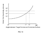
- FIG. 10 shows simulated data for defect density as a function of sputtering angle.
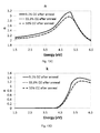
- FIGS. 11A and B show X-ray photoelectron spectra of tantalum oxide layers made with low oxygen concentration in a dc reactive sputtering chamber.
- FIGS. 12A and B show deep UV spectroscopic ellipsometry measurements of tantalum oxide layers made with varying oxygen concentrations in a dc reactive sputtering chamber.
- FIGS. 13A-D show deep UV spectroscopic ellipsometry measurements of tantalum oxide layers made with higher oxygen concentrations in a dc reactive sputtering chamber.
- FIG. 14 shows tantalum oxide deposition rate as a function of O 2 concentration at 100 W power using dc reactive sputtering.
- this invention is not limited to specific resistive switching layer or resistive layer compositions. Exemplary embodiments will be described for a plurality of layers comprising Ta 2 O 5- ⁇ (near stoichiometric, bistable resistance) layers and TaO 2.5-x (substoichiometric, resistive) layers, but bilayers and multilayers comprising stoichiometric, near-stoichiometric, and substoichiometric oxides, nitrides, and oxynitrides of any metal can beneficially be produced using the methods disclosed herein.
- the layers can comprise compounds of the form Me 1 w Me 2 x Si y O z N v , where Me 1 and Me 2 are metals, v ⁇ 0, w ⁇ 0, x ⁇ 0, y ⁇ 0, and z>0, and at least one of w, x, and y is greater than zero. It is also to be understood that the terminology used herein is for the purpose of describing particular embodiments only and is not intended to limit the scope of the present invention.
- near-stoichiometric refers to compounds where the atomic ratio deviates only slightly from the stoichiometrically correct ratio (wherein valence electrons are all balanced).
- valence electrons are all balanced.
- near-stoichiometric metal oxides described herein there is typically a slight deficit of oxygen atoms relative to that of the fully oxidized metal, that deficit being sufficient to create defects in the lattice and a bistable resistance characteristic in sufficiently thin layers.
- such near-stoichiometric oxides are abbreviated by adding a “ ⁇ ” after the number of oxygen atoms in an otherwise stoichiometric formula (e.g., Ta 2 O 5- ⁇ ).
- the term “substoichiometric” refers to compounds where the atomic ratio deviates substantially (more than 0.01%) from the stoichiometrically correct ratio.
- substoichiometric oxides described herein there is a larger deficit of oxygen atoms (compared to near-stoichiometric oxides) sufficient to create continuous permanent strings of defects in the lattice and a linear resistance characteristic.
- such oxides are abbreviated by adding a “ ⁇ x” after the relative number of oxygen atoms in a formula where the count of metal atoms is taken to be 1 (e.g., TaO 2.5-x ).
- oxynitride refers to embodiments of near-stoichiometric or substoichiometric oxides containing nitrogen, for example, Ta 2 O 5- ⁇ N y or TaO 2.5-x N y , respectively.
- the value of y is less than or equal to ⁇ or x, typically somewhat less, although y can be adjusted independently of ⁇ or x to achieve particular performance characteristics for the resultant layer.
- nitrogen-stabilized oxide is a synonym of “oxynitride” reflecting the possibility that an oxide layer is “stabilized” by adding nitrogen atoms to replace a subset of the oxygen vacancies.
- the term “conductor” refers to a volume of material (such as a wire, thin film, or electrode) comprising a “conductive material.”
- the material is said to be “conductive” if there is negligible voltage drop across the conductor at operating currents. In certain instances, a small voltage drop is acceptable, although typically the voltage drop across adjacent components is much larger.
- Embodiments of the present invention relate to nonvolatile memory formed from resistive switching elements. Embodiments of the invention also relate to fabrication methods that may be used to form nonvolatile memory having resistive switching memory elements.
- Resistive switching elements may be formed on any suitable type of integrated circuit. Most typically, resistive switching memory elements may be formed as part of a high-capacity nonvolatile memory integrated circuit.
- Nonvolatile memory integrated circuits are often used as data storage devices in portable and non-portable computing machines as well as portable devices such as digital cameras, mobile telephones, handheld computers, vehicles, appliances, and music players.
- Nonvolatile memory devices are packaged in memory cards or memory keys that can be removably installed in electronic equipment by a user.
- resistive switching memory elements to form memory arrays on memory devices are merely illustrative. In general, any suitable integrated circuit may be formed using the resistive switching structures of the present invention. Fabrication of memory arrays formed of resistive switching memory elements is described herein as an example.
- Resistive random access memory Memory arrays formed of resistive switching memory elements are known as “resistive random access memory” or “ReRAM.”
- the first electrodes of each nonvolatile memory element are coplanar and arranged as a first set of parallel electrodes
- the second electrodes of each nonvolatile memory element are coplanar and arranged as a second set of parallel electrodes at an angle to the first set of parallel electrodes.
- FIG. 1 An illustrative memory array 10 of resistive switching memory elements 12 is shown in FIG. 1 .
- Memory array 10 may be part of a memory device or other integrated circuit. Read and write circuitry is connected to memory elements 12 using conductors 16 and orthogonal conductors 18 . Conductors such as conductors 16 and conductors 18 are sometimes referred to as word lines and bit lines and are used to read and write data into the elements 12 of array 10 . Individual memory elements 12 or groups of memory elements 12 can be addressed using appropriate sets of conductors 16 and 18 .
- Memory element 12 may be formed from one or more layers of materials, as indicated schematically by lines 14 in FIG. 1 . In addition, the memory arrays shown can be stacked in a vertical fashion to make multi-layer 3-D memory arrays.
- the state of a memory element 12 can be sensed by applying a sensing voltage to an appropriate set of conductors 16 and 18 .
- a memory element that is addressed in this way may be in either a high resistance state or a low resistance state.
- the resistance of the memory element therefore determines what digital data is being stored by the memory element. If the memory element has a high resistance, for example, the memory element may be said to contain a logic one (i.e., a “1” bit). If, on the other hand, the memory element has a low resistance, the memory element may be said to contain a logic zero (i.e., a “0” bit).
- the state of a memory element can be changed by application of suitable write signals to an appropriate set of conductors 16 and 18 .
- FIG. 2A A cross-section of an illustrative embodiment of a resistive switching memory element is shown in FIG. 2A .
- memory element 12 (as shown in FIG. 1 ) is formed from a metal oxide memory layer 22 and has conductive electrodes 20 and 24 .
- conductive lines such as lines 16 and 18 may be physically and electrically connected to electrodes 20 and 24 .
- Such conductive lines may be formed from any suitable metals (e.g., tungsten, aluminum, copper, metal silicides, etc.).
- Conductive lines 16 and 18 may also be formed from other conductive materials (e.g., doped polysilicon, doped silicon, etc.), combinations of these materials, or any other suitable conductive material. If desired, conductive line 16 and conductive line 18 may serve as both conductive lines and as electrodes. In this type of arrangement, line 16 may serve as electrode 20 , so that no separate conductor is needed to form an upper electrode for element 12 . Similarly, line 18 may serve as electrode 24 , so that no separate conductor is needed for the lower electrode of element 12 .
- conductive lines 16 and 18 are shown schematically as being formed in contact with electrodes 20 and 24 .
- Other arrangements may be used if desired.
- there may be intervening electrical components e.g., resistors, diodes, transistors, etc. that are formed between line 16 and electrode 20 or between line 18 and electrode 24 .
- an intervening electrical component between an electrode and resistive switching layer 22 .
- An illustrative arrangement in which there is an intervening electrical component 38 between electrode 24 and metal oxide 22 is shown in FIG. 2B .
- conductive materials such as electrodes 24 and 20 may be formed from one or more layers of materials.
- materials that may be used to form electrodes 20 and 24 include metal (e.g., refractory or transition metals), metal alloys, metal nitrides (e.g., refractory metal nitrides), metal silicon nitrides (i.e., materials containing refractory metals, transition metals, or other metals, along with silicon, and nitrogen), metal silicides, or other conductors.
- a titanium nitride layer or similar barrier layer under lower electrode 24 can be added to prevent metals and other doping and alloying elements from diffusing into an underlying silicon structure.
- Resistive switching memory element 12 exhibits a bistable resistance. When resistive switching memory element 12 is in a high resistance state, it may be said to contain a logic one. When resistive switching memory element 12 is in a low resistance state, it may be said to contain a logic zero. (If desired, high resistance can signify a logic zero and low resistance can signify a logic one.) The state of resistive switching memory element 12 may be sensed by application of a sensing voltage. When it is desired to change the state of resistive switching memory element 12 , read and write circuitry may apply suitable control signals across terminals 16 and 18 .
- FIG. 3 A current (I) versus voltage (V) plot for memory element 12 is shown in FIG. 3 .
- memory element 12 may be in a high resistance state (e.g., storing a logic one). In this state, the current versus voltage characteristic of memory element 12 is represented by solid line HRS 26 .
- the high resistance state of memory element 12 can be sensed by read and write circuitry. For example, read and write circuitry may apply a read voltage V read to memory element 12 and can sense the resulting low current I L that flows through memory element 12 . When it is desired to store a logic zero in memory element 12 , memory element 12 can be placed into its low-resistance state.
- V set may be applied across terminals 16 and 18 of memory element 12 .
- Applying V set to memory element 12 causes memory element 12 to enter its low resistance state, as indicated by dotted line 30 .
- the structure of memory element 12 is changed (e.g., through the formation of current filaments through memory layer 22 or other suitable mechanisms), so that, following removal of the voltage V set , memory element 12 is characterized by low resistance curve LRS 28 .
- the low resistance state of memory element 12 can be sensed using read and write circuitry.
- read and write circuitry When a read voltage V read is applied to resistive switching memory element 12 , read and write circuitry will sense the relatively high current value I H , indicating that memory element 12 is in its low resistance state.
- the memory element can once again be placed in its high resistance state by applying a voltage V reset to memory element 12 .
- V reset When read and write circuitry applies V reset to memory element 12 , memory element 12 enters its high resistance state HRS, as indicated by dotted line 32 .
- the voltage V reset is removed from memory element 12 , memory element 12 will once again be characterized by high resistance line HRS 26 .
- Example 4 shows measurements on two different embodiments of resistive switching memory element 12 . In the example, V set and V reset are in the range 1-4 V, and V read is about 0.5 V.
- bistable resistance of resistive switching memory element 12 makes memory element 12 suitable for storing digital data. Because no changes take place in the stored data in the absence of application of the voltages V set and V reset , memory formed from elements such as memory element 12 is nonvolatile.
- Any suitable read and write circuitry and array layout scheme may be used to construct a nonvolatile memory device from resistive switching memory elements such as memory element 12 .
- resistive switching memory elements such as memory element 12 .
- horizontal and vertical lines 16 and 18 may be connected directly to the terminals of resistive switching memory elements 12 .
- other electrical devices may be associated with each memory element 12 .
- Diode 36 may be placed in series with resistive switching memory element 12 .
- Diode 36 may be a Schottky diode, a p-n diode, a p-i-n diode, or any other suitable diode.
- resistive switching memory element 12 can be formed in series with resistive switching memory element 12 .
- electrical device 38 may be placed in series with resistive switching memory element 12 .
- Device 38 may be a resistor, a diode, a transistor, or any other suitable electronic device. Because devices such as these can rectify or otherwise alter current flow, these devices are sometimes referred to as rectifying elements or current steering elements.
- two electrical devices 38 may be placed in series with a resistive switching memory element 12 .
- Memory elements 12 may be formed in a single layer in array 10 or may be formed in multiple layers.
- An advantage of forming memory arrays such as memory array 10 of FIG. 1 using a multi-layer memory element scheme is that this type of approach allows memory element density to be maximized.
- a resistive switching metal oxide layer may be formed above or below a diode (as an example).
- Conductive lines 16 and 18 may be electrically coupled to metal oxide layer 22 through a number of layers of conductive material. There may, in general, be any suitable number of conductive layers associated with resistive switching memory element 12 .
- These conductive layers may be used for functions such as adhesion promotion, seed layers for subsequent electrochemical deposition, diffusion barriers to prevent undesired materials from diffusing into adjacent structures, contact materials (e.g., metals, metal alloys, metal nitrides, etc.) for forming ohmic contacts with the metal oxide 22 , contact materials (e.g., metals, metal alloys, metal nitrides, etc.) for forming Schottky contacts to the metal oxide 22 , etc.
- contact materials e.g., metals, metal alloys, metal nitrides, etc.
- the conductive layers in memory element 12 may be formed from the same conductive material or different conductive materials. Moreover, conductive layers in memory element 12 may be formed using the same techniques or different techniques. As an example, one layer of a conductor may be formed using physical vapor deposition (PVD) techniques (e.g., sputter deposition), whereas another layer of a conductor may be formed using electrochemical deposition.
- PVD physical vapor deposition
- electrochemical deposition e.g., electrochemical deposition
- the portions of the conductive layers in memory element 12 that are immediately adjacent to metal oxide 22 or are otherwise in close association with metal oxide 22 are sometimes referred to as the electrodes of the resistive switching memory element 12 .
- the electrodes of resistive switching memory element 12 may each include a single material (e.g., tantalum), may each include multiple materials (e.g., tantalum and titanium nitride), may include materials formed using different techniques (e.g., electrochemically deposited tantalum and PVD tantalum), or may include combinations of such materials.
- metal oxides are particularly appropriate for forming the resistive switching metal oxide layer 22 .
- These metal oxides may include, for example, the transition metal oxides and mixtures thereof.
- oxides and oxynitrides of tantalum, niobium, hafnium, yttrium, zirconium, lanthanum, vanadium, titanium, tungsten, nickel, aluminum, and silicon, and combinations thereof can be used in forming the resistive switching metal oxide layer.
- tantalum oxide is used in forming the resistive switching metal oxide layer.
- Any suitable conductive materials may be used for forming the electrodes 20 and 24 of resistive switching memory element 12 .
- Illustrative conductive materials include transition metals (and their nitrides), refractory metals (and their nitrides), and noble metals.
- Illustrative examples of conductive materials include Ti, Ta, W, Mo, Hf, Nb, Ni, Pd, Pt, Re, Ru, and Ir.
- Illustrative metal nitrides include titanium nitride, tantalum nitride, tungsten nitride, and molybdenum nitride. These are merely illustrative examples of materials that may be used for electrodes 20 and 24 . Combinations of two or more of these materials (and/or their nitrides) metals may be used or other suitable conductive materials may be used as electrodes 20 and 24 , if desired.
- the electrodes 20 and 24 and other conductive layers that may be associated with memory element 12 may be formed using any suitable techniques.
- Illustrative conductive material fabrication techniques include physical vapor deposition (e.g., sputter deposition, evaporation), chemical vapor deposition, atomic layer deposition, and electrochemical deposition (e.g., electroless deposition, electroplating).
- nonvolatile memory elements comprise a first electrode layer, a second electrode layer, and a first oxide layer and second oxide layer disposed between the first and second electrode layers.
- the first oxide layer comprises Me 1 w Me 2 x Si y O z , where Me 1 and Me 2 are metals, w ⁇ 0, x ⁇ 0, y ⁇ 0, and z>0, and at least one of w, x, and y is greater than zero
- the second oxide layer comprises Me 1 a Me 2 b Si c O d , where a ⁇ 0, b ⁇ 0, c ⁇ 0, and d>0, and at least one of a, b, and c is greater than zero.
- One of the oxide layers has linear resistance and substoichiometric composition, and the other oxide layer has bistable resistance and near-stoichiometric composition.
- the oxide layers can further comprise nitrogen.
- the sum of the two oxide layer thicknesses is between about 20 ⁇ and about 100 ⁇ , and the layer with bistable resistance has a thickness between about 25% and about 75% of the total thickness.
- the first electrode layer comprises doped polycrystalline silicon and the second electrode layer comprises titanium nitride.
- the layer with bistable resistance is adjacent to the first electrode layer.
- the layer with bistable resistance is adjacent to the second electrode layer.
- Arrays of nonvolatile memory elements can be prepared to provide memory devices comprising the memory elements.
- the combination of a memory layer 22 and a fixed resistor 38 can be formed as a bilayer.
- Exemplary embodiments of transition metal oxides herein generally comprise tantalum oxide, but other oxides and oxynitrides of transition metals such as niobium, hafnium, yttrium, zirconium, lanthanum, vanadium, titanium, tungsten, and nickel, as well as oxides and oxynitrides of aluminum and silicon, and combinations thereof can also be used.
- Each bilayer comprises one layer of near-stoichiometric composition having bistable resistance used as a memory layer and forming memory element 12 together with one layer of substoichiometric composition having linear resistance used as fixed resistor 38 .
- the combined thickness of the layers is generally in the range 20-100 ⁇ , and the relative thickness of the two layers can be between 1:3 and 3:1.
- a preferred embodiment providing an attractive combination of performance characteristics and packaged memory density has a total layer thickness of 50-100 ⁇ ; the memory layer comprises one quarter of the total thickness.
- such structures can be made with operating voltages and currents that are consistent with common semiconductor technologies.
- arrays of memory elements can readily be made using any available fabrication line widths. The memory elements require few layers, and the layers are generally thin compared to line widths. Devices that are competitive with any semiconductor or disk memory technology can be designed with fast access speeds and high memory capacity (e.g., >1 Tbyte).
- methods are provided of forming a plurality of layers to manufacture a resistive switching nonvolatile memory element.
- the method can comprise forming a first layer on a substrate, wherein the first layer comprises Me 1 w Me 2 x Si y O z , where Me 1 and Me 2 are metals, w ⁇ 0, x ⁇ 0, y ⁇ 0, and z>0, and at least one of w, x, and y is greater than zero; and forming a second layer on a substrate, wherein the second layer comprises Me 1 a Me 2 b Si c O d , where a ⁇ 0, b ⁇ 0, c ⁇ 0, and d>0 and at least one of a, b, and c is greater than zero.
- the layers are formed using reactive sputtering in an atmosphere with controlled amounts of argon and oxygen.
- the sputtering atmosphere is performed at reduced pressure, such as between about 1 mTorr and about 5 mTorr.
- the layers can be formed using ALD or CVD.
- At least two layers are deposited, where one layer has linear resistance and substoichiometric composition, and the other layer has bistable resistance and near-stoichiometric composition.
- the oxygen concentration of the atmosphere used to form the layer having linear resistance is typically less than about 5 volume percent, while the oxygen concentration of the atmosphere used to form the layer having bistable resistance is typically more than about 30 volume percent.
- the sum of the two layer thicknesses is between about 20 ⁇ and about 100 ⁇ , and the layer with bistable resistance has a thickness between 25% and 75% of the total thickness.
- the first layer can be formed using sputtering, wherein the first layer comprises Me 1 w Me 2 x Si y , where Me 1 and Me 2 are metals, w ⁇ 0, x ⁇ 0, y ⁇ 0, and at least one of w, x, and y is greater than zero.
- the second layer can be formed above or below the first layer using reactive sputtering in an atmosphere comprising argon and oxygen, wherein the second layer comprises Me 1 a Me 2 b Si c O d , where a ⁇ 0, b ⁇ 0, c ⁇ 0, and d>0, and at least one of a, b, and c is greater than zero.
- the first layer is formed in the absence of a reactive gas such as O 2 or N 2 , while the second layer is formed in the presence of a reactive gas.
- the oxygen concentration of the atmosphere used to form the second layer is typically more than about 30 volume percent.
- nitrogen can also be present in the second layer (e.g., by including nitrogen as a component of the reactive gas).
- the methods further comprise annealing the first and second layers such that oxygen atoms migrate from the second layer into the first layer.
- the subsequent annealing can cause some 0 (or N) migration into the pure metal layer to create a metal-rich oxide (or oxynitride).
- the annealed first layer has linear resistance and substoichiometric composition
- the annealed second layer has bistable resistance and near-stoichiometric composition.
- the layers can be formed in any order.
- the sum of the two layer thicknesses is between about 20 ⁇ and about 100 ⁇
- the second layer has a thickness between 25% and 75% of the total thickness.
- the metal is a transition metal, such as tantalum or niobium.
- the metal is selected from the group consisting of tantalum, niobium, hafnium, yttrium, zirconium, lanthanum, vanadium, titanium, tungsten, nickel, aluminum, and combinations thereof.
- the transition metal is tantalum provided by reactive sputtering (dc, ac, or rf) from a tantalum target. To form tantalum oxide species, the reactive sputtering is performed in an Ar/O 2 atmosphere. A typical pressure of the Ar/O 2 atmosphere is 1-5 mTorr.
- tantalum oxide layers of varying stoichiometry are formed by varying the oxygen concentration during the sputtering process. Tantalum most commonly has five valence electrons (5 d 3 6 s 2 ), and Ta 2 O 5 is the typical stable oxide. However, when the O 2 level in the sputtering chamber is insufficient to provide all of the oxygen atoms necessary to form Ta 2 O 5 , suboxides can be formed. Suboxides of tantalum are formed when the oxygen concentration is less than about 5%. Layers formed at 5% O 2 have mixed oxide composition and linear resistance. The oxygen concentration used to form near-stoichiometric Ta 2 O 5- ⁇ layers having bistable resistance is more than about 30%. Similar results were observed in niobium oxides as well using the same oxygen concentrations.
- X-ray Photoelectron Spectroscopy shows that both TaO 2 and TaO can be formed when the O 2 level is kept low. Annealing (at least 1 min at at least 750 C in an Ar/H 2 atmosphere) can reduce or eliminate these suboxides as shown in Example 2.
- Substoichiometric tantalum oxide can also exist as Ta 2 O 5 with interstitial Ta atoms present.
- a typical array of nonvolatile memory elements assembled with crossed parallel electrodes requires individual steering elements such as p-i-n diodes for each memory element.
- the annealing process mentioned above (750 C for 1 min in Ar/H 2 ) is typically used to enable migration of dopant atoms in the steering elements. This annealing is typically performed after all device layers are formed.
- the substoichiometric and near-stoichiometric layers are protected from the above-mentioned changes in stoichiometry on annealing, because the production annealing occurs after the top electrode layer (e.g., TiN) is formed, and this top electrode layer protects the oxide layer from exposure to the Ar/H 2 atmosphere.
- the top electrode layer e.g., TiN
- Typical operating conditions for the sputtering process comprise total pressures of 1-5 mTorr. If the O 2 concentration exceeds about 33%, the oxide approaches stoichiometric composition. At lower O 2 concentrations, increasing amounts of substoichiometric oxides can be formed in a well-controlled fashion as indicated in Examples 1 and 2.
- Example 3 shows the results of deep UV spectroscopic ellipsometry measurements of dielectric properties of these substoichiometric oxide layers which confirm the presence of metal rich material.
- N 2 can be added to the Ar/O 2 gas mix to obtain oxynitrides such as Ta 2 O 5- ⁇ N y or TaO 2.5-x N y .
- the value of y is less than or equal to ⁇ or x, typically somewhat less, although y can be adjusted independently of ⁇ or x to achieve particular performance characteristics for the resultant layer.
- the presence of N atoms can stabilize the O vacancies and improve the endurance of switching and data retention time with lower transient switching currents.
- these “oxynitrides” can also be described as “nitrogen stabilized oxides,” and the two terms will be used interchangeably herein.
- Tantalum nitride is a good conductor with metallic conduction behavior (i.e., free electrons), and thus the addition of N atoms can stabilize the structure while still allowing conduction filaments to be created and destroyed.
- Nitrogen stabilization can, for example, enable the use of lower set and reset voltages and improve the number of set/reset cycles that can be reliably sustained in a layer with bistable resistance. With respect to sub-stoichiometric resistive layers, nitrogen atoms can stabilize the structure against changes in resistance due to oxygen vacancy migration and can be used to assist in tuning the resistivity of the layers.
- similar metal or silicon oxide, nitride, and oxynitride layers can be formed using Atomic Layer Deposition (ALD) or Chemical Vapor Deposition (CVD).
- ALD Atomic Layer Deposition
- CVD Chemical Vapor Deposition
- tantalum oxides can be formed using pentakis(dimethylamino)tantalum as a tantalum precursor and ozone as a reactant gas to supply oxygen.
- the layers can be formed by providing alternating pulses of the precursor gas and reactant gas to build sub-monolayer thicknesses per pulse.
- CVD both gases can be supplied simultaneously. Stoichiometric control can be implemented, for example, by controlling the temperature of the bubbler.
- the pentakis(dimethylamino)tantalum precursor is supplied as a liquid through which a carrier gas such as N 2 is passed, and the temperature of the liquid determines the amount of precursor entrained.
- a carrier gas such as N 2
- the pulse (exposure) time can also be varied as can the choice of reactant gas.
- H 2 O can be used instead of O 3 as a reactant gas for supplying oxygen in order to form more metal-rich layers.
- the pressure in the sputtering chamber is increased significantly from the normal operating point.
- the oxygen content of the formed layer can be varied by varying the O 2 concentration in the Ar/O 2 atmosphere.
- the resulting layer resistivity is shown qualitatively in FIG. 7 , where the “Low Pressure” curve corresponds roughly to typical operating conditions. (Data shown are simulations and do not represent real data for any particular metal oxide, sputtering power, or any particular operating pressure.)
- resistivity is a steep function of the oxygen flow rate in a range C1-C2, and accurate control of resistivity would be very difficult.
- the substrate bias applied during sputtering is adjusted in an abnormal way.
- a typical (simulation) example of how oxide layer resistivity varies with substrate bias is shown in FIG. 8 .
- the substrate bias is selected to maximize layer density through ion bombardment. Maximum layer density correlates with minimum resistivity. The layer density decreases to either side of this “optimum” substrate bias. In both directions, the resistivity in the layer increases. While there is a limit to the resistivity that can be achieved at low substrate bias, there is no such limit to the high side, and, in principle, arbitrary layer resistivity can be achieved. In practice, depending on other process parameters, the curve may become too steep in the target range, and this method can usefully be combined with the first and/or third methods to optimize process control.
- the sputter gun is positioned at an oblique angle, for example, greater than about 55° from the substrate normal (e.g., from about 55° to about 85°).
- the typical position of the sputter gun is directly overhead at 90° from the substrate plane.
- the reduced normal momentum from atoms incident at a glancing angle can also increase defect density and therefore resistivity to provide an additional control parameter.
- bilayers and multilayers of varying composition and thickness can be created using any of the above-described methods for the deposition of each layer and adjusting the deposition time and/or sputtering conditions to obtain target layer thicknesses. Additional layers can be formed if desired.
- Tantalum oxide layers of varying composition were made by dc reactive sputtering in a locally built chamber as described above using either 4.3% or 5.4% O 2 in Ar (generally at 1-5 mTorr and 100-300 W). (All relative concentrations are set as volume flow rates such as standard cubic centimeters per minute [sccm].) These layers were expected to have substoichiometric composition. The layers were analyzed using XPS. The spectra of two samples are shown in FIGS. 11A and B, respectively, together with the peaks associated with a least-squares fit of possible constituents. The overall fit to the data is very good. Table 1 summarizes the compositional analysis:
- Example 1 The samples described in Example 1 were further analyzed using deep UV spectral ellipsometry. Each sample was analyzed before and after annealing for 1 min at 750 C in an Ar/H 2 atmosphere. The results are shown in FIGS. 12A and B and 13 A-D. ‘n’ and ‘k’ are the refractive index and extinction coefficient respectively.
- the samples made with O 2 concentrations below 10% show significant absorption at lower energies, indicative of metallic or low band-gap suboxide phases. These are reduced but not eliminated after anneal. At higher O 2 concentrations these lower energy absorptions are absent.
- FIG. 14 shows that such control is indeed possible.
- the data are for 100 W power in a dc reactive sputtering process as a function of the O 2 concentration in the Ar/O 2 atmosphere. While the deposition rate for the lower O 2 concentrations is significantly higher than for higher concentrations, all rates are acceptably low to allow precise thickness control.
- a series of bilayer structures were deposited between a base conductor of positively doped polysilicon and top conductor of TiN. Standard semiconductor fabrication methods were used to create a variety of test samples on a wafer. Layers were formed using Atomic Layer Deposition (ALD) and Physical Vapor Deposition (PVD—e.g., reactive sputtering). Electrodes and other patterned structures were created as needed by photolithography and dry etching. Each wafer was cleaved into “coupons” with 2-4 “dies” each.
- Varying thicknesses of a substoichiometric TaO 2.5-x layer (formed at 4% O 2 concentration) and a near-stoichiometric Ta 2 O 5- ⁇ layer (formed at 50% O 2 concentrations) were tested, where the combined thickness of the oxide layers was 20-100 ⁇ , and the relative thickness of the two layers was approximately 1:3, 1:1, or 3:1.
- a preferred embodiment providing an attractive combination of performance characteristics and packaged memory density was found to be one where the total oxide thickness was 50-100 ⁇ , and the near-stoichiometric (bistable resistance) layer thickness was about 25% of the total.
- Sample electrical measurements on samples with 75 ⁇ of a TaO 2.5-x resistor layer and 25 ⁇ of a Ta 2 O 5- ⁇ bistable memory layer are shown in Table 3. Results are shown for both memory layer on the top and memory layer on the bottom. Median values are shown. The overall yield of testable bilayer structures was 100%.
- V forming is the voltage required to form a conductive filament for the first time through the memory layer.
- V reset and V set are the voltages required to break and reform the filaments during normal memory use measured across the near-stoichiometric memory layer. (Real circuits would have additional voltage drop across other resistances).
- the state of the memory layer can be read with a voltage of about 0.5 V. Note that there is a particularly significant difference between the set currents for the two geometries. There is also a marked difference between the forming voltages. Both show that the memory-layer-on-top arrangement is advantageous from a device performance point of view. The only asymmetry that makes the two geometries functionally different is the different materials used for the top and bottom electrodes.
- the lower set current required for the memory-layer-on-top arrangement provides evidence that the enablement of migration of oxygen vacancies in and out of an adjacent TiN layer is advantageous.
Landscapes
- Engineering & Computer Science (AREA)
- Manufacturing & Machinery (AREA)
- Chemical & Material Sciences (AREA)
- Materials Engineering (AREA)
- Semiconductor Memories (AREA)
Abstract
Description
| TABLE 1 | |||||
| % O2 in Ar carrier gas | % Ta2O5 | % TaO2 | % TaO | ||
| 4.3 | 83 | 10 | 7 | ||
| 5.4 | 86 | 8 | 6 | ||
| TABLE 2 | |||
| % O2 in Ar carrier gas | % Ta2O5 | ||
| 10 | 93 | ||
| 33 | 100 | ||
| 50 | 100 | ||
| TABLE 3 | ||
| Parameter | Memory Layer on Top | Memory Layer on Bottom |
| Vforming | 4.88 | V | 6.15 | V |
| Vset | 2.23 | V | 3.70 | V |
| Iset | 51 | μA | 131 | μA |
| Vreset | −1.25 | V | −1.19 | V |
| Ireset | −210 | μA | −230 | μA |
Claims (18)
Priority Applications (5)
| Application Number | Priority Date | Filing Date | Title |
|---|---|---|---|
| US13/367,927 US8569104B2 (en) | 2012-02-07 | 2012-02-07 | Transition metal oxide bilayers |
| PCT/US2013/025238 WO2013119882A1 (en) | 2012-02-07 | 2013-02-07 | Transition metal oxide bilayers |
| US13/971,467 US8704203B2 (en) | 2012-02-07 | 2013-08-20 | Transition metal oxide bilayers |
| US14/252,285 US8987697B2 (en) | 2012-02-07 | 2014-04-14 | Transition metal oxide bilayers |
| US14/618,055 US9087978B1 (en) | 2012-02-07 | 2015-02-10 | Transition metal oxide bilayers |
Applications Claiming Priority (1)
| Application Number | Priority Date | Filing Date | Title |
|---|---|---|---|
| US13/367,927 US8569104B2 (en) | 2012-02-07 | 2012-02-07 | Transition metal oxide bilayers |
Related Child Applications (1)
| Application Number | Title | Priority Date | Filing Date |
|---|---|---|---|
| US13/971,467 Continuation US8704203B2 (en) | 2012-02-07 | 2013-08-20 | Transition metal oxide bilayers |
Publications (2)
| Publication Number | Publication Date |
|---|---|
| US20130200324A1 US20130200324A1 (en) | 2013-08-08 |
| US8569104B2 true US8569104B2 (en) | 2013-10-29 |
Family
ID=48902110
Family Applications (4)
| Application Number | Title | Priority Date | Filing Date |
|---|---|---|---|
| US13/367,927 Expired - Fee Related US8569104B2 (en) | 2012-02-07 | 2012-02-07 | Transition metal oxide bilayers |
| US13/971,467 Active US8704203B2 (en) | 2012-02-07 | 2013-08-20 | Transition metal oxide bilayers |
| US14/252,285 Expired - Fee Related US8987697B2 (en) | 2012-02-07 | 2014-04-14 | Transition metal oxide bilayers |
| US14/618,055 Expired - Fee Related US9087978B1 (en) | 2012-02-07 | 2015-02-10 | Transition metal oxide bilayers |
Family Applications After (3)
| Application Number | Title | Priority Date | Filing Date |
|---|---|---|---|
| US13/971,467 Active US8704203B2 (en) | 2012-02-07 | 2013-08-20 | Transition metal oxide bilayers |
| US14/252,285 Expired - Fee Related US8987697B2 (en) | 2012-02-07 | 2014-04-14 | Transition metal oxide bilayers |
| US14/618,055 Expired - Fee Related US9087978B1 (en) | 2012-02-07 | 2015-02-10 | Transition metal oxide bilayers |
Country Status (2)
| Country | Link |
|---|---|
| US (4) | US8569104B2 (en) |
| WO (1) | WO2013119882A1 (en) |
Cited By (20)
| Publication number | Priority date | Publication date | Assignee | Title |
|---|---|---|---|---|
| US20130270509A1 (en) * | 2012-04-17 | 2013-10-17 | Gwangju Institute Of Science And Technology | Resistance change memory device having threshold switching and memory switching characteristics, method of fabricating the same, and resistance change memory device including the same |
| US20140145135A1 (en) * | 2011-06-30 | 2014-05-29 | Crossbar, Inc. | Sub-oxide interface layer for two-terminal memory |
| US9543359B2 (en) | 2011-05-31 | 2017-01-10 | Crossbar, Inc. | Switching device having a non-linear element |
| US9564587B1 (en) | 2011-06-30 | 2017-02-07 | Crossbar, Inc. | Three-dimensional two-terminal memory with enhanced electric field and segmented interconnects |
| US9570678B1 (en) | 2010-06-08 | 2017-02-14 | Crossbar, Inc. | Resistive RAM with preferental filament formation region and methods |
| US9576616B2 (en) | 2012-10-10 | 2017-02-21 | Crossbar, Inc. | Non-volatile memory with overwrite capability and low write amplification |
| US9583701B1 (en) | 2012-08-14 | 2017-02-28 | Crossbar, Inc. | Methods for fabricating resistive memory device switching material using ion implantation |
| US9590013B2 (en) | 2010-08-23 | 2017-03-07 | Crossbar, Inc. | Device switching using layered device structure |
| USRE46335E1 (en) | 2010-11-04 | 2017-03-07 | Crossbar, Inc. | Switching device having a non-linear element |
| US9601692B1 (en) | 2010-07-13 | 2017-03-21 | Crossbar, Inc. | Hetero-switching layer in a RRAM device and method |
| US9620206B2 (en) | 2011-05-31 | 2017-04-11 | Crossbar, Inc. | Memory array architecture with two-terminal memory cells |
| US9627443B2 (en) | 2011-06-30 | 2017-04-18 | Crossbar, Inc. | Three-dimensional oblique two-terminal memory with enhanced electric field |
| US9633723B2 (en) | 2011-06-23 | 2017-04-25 | Crossbar, Inc. | High operating speed resistive random access memory |
| US9673255B2 (en) | 2012-04-05 | 2017-06-06 | Crossbar, Inc. | Resistive memory device and fabrication methods |
| US9685608B2 (en) | 2012-04-13 | 2017-06-20 | Crossbar, Inc. | Reduced diffusion in metal electrode for two-terminal memory |
| US9735358B2 (en) | 2012-08-14 | 2017-08-15 | Crossbar, Inc. | Noble metal / non-noble metal electrode for RRAM applications |
| US9741765B1 (en) | 2012-08-14 | 2017-08-22 | Crossbar, Inc. | Monolithically integrated resistive memory using integrated-circuit foundry compatible processes |
| US9793474B2 (en) | 2012-04-20 | 2017-10-17 | Crossbar, Inc. | Low temperature P+ polycrystalline silicon material for non-volatile memory device |
| US9972778B2 (en) | 2012-05-02 | 2018-05-15 | Crossbar, Inc. | Guided path for forming a conductive filament in RRAM |
| US10290801B2 (en) | 2014-02-07 | 2019-05-14 | Crossbar, Inc. | Scalable silicon based resistive memory device |
Families Citing this family (7)
| Publication number | Priority date | Publication date | Assignee | Title |
|---|---|---|---|---|
| US8896521B2 (en) * | 2012-04-24 | 2014-11-25 | Qualcomm Mems Technologies, Inc. | Metal-insulator-metal capacitors on glass substrates |
| US10115671B2 (en) | 2012-08-03 | 2018-10-30 | Snaptrack, Inc. | Incorporation of passives and fine pitch through via for package on package |
| US20140273525A1 (en) * | 2013-03-13 | 2014-09-18 | Intermolecular, Inc. | Atomic Layer Deposition of Reduced-Leakage Post-Transition Metal Oxide Films |
| FR3027453B1 (en) * | 2014-10-20 | 2017-11-24 | Commissariat Energie Atomique | RESISTIVE DEVICE FOR MEMORY OR LOGIC CIRCUIT AND METHOD FOR MANUFACTURING SUCH A DEVICE |
| US9947721B2 (en) * | 2016-04-01 | 2018-04-17 | Micron Technology, Inc. | Thermal insulation for three-dimensional memory arrays |
| US10468458B2 (en) * | 2016-05-10 | 2019-11-05 | Winbond Electronics Corp. | Resistive random access memory having selector and current limiter structures |
| WO2021022410A1 (en) * | 2019-08-02 | 2021-02-11 | 北京大学 | Resistive random access memory operation circuit and operation method |
Citations (1)
| Publication number | Priority date | Publication date | Assignee | Title |
|---|---|---|---|---|
| US20070107774A1 (en) * | 2004-07-22 | 2007-05-17 | Pfleiderer Water Systmes Gmbh | Bistable resistance value acquisition device, manufacturing method thereof, metal oxide thin film, and manufacturing method thereof |
Family Cites Families (16)
| Publication number | Priority date | Publication date | Assignee | Title |
|---|---|---|---|---|
| US4405421A (en) * | 1980-02-22 | 1983-09-20 | Inoue-Japax Research Incorporated | Method of and apparatus for electrochemically grinding a conductive workpiece |
| US4931213A (en) * | 1987-01-23 | 1990-06-05 | Cass Richard B | Electrically-conductive titanium suboxides |
| DE69125323T2 (en) * | 1990-07-24 | 1997-09-25 | Semiconductor Energy Lab | Methods of making insulating films, capacitors, and semiconductor devices |
| KR100297628B1 (en) * | 1998-10-09 | 2001-08-07 | 황 철 주 | Method for manufacturing semiconductor devices |
| US6649502B2 (en) * | 2000-05-16 | 2003-11-18 | Samsung Electronics Co., Ltd. | Methods of forming multilayer dielectric regions using varied deposition parameters |
| FR2835534B1 (en) * | 2002-02-06 | 2004-12-24 | Saint Gobain | NON STOECHIOMETRIC CERAMIC TARGET NiOx |
| US20050252449A1 (en) * | 2004-05-12 | 2005-11-17 | Nguyen Son T | Control of gas flow and delivery to suppress the formation of particles in an MOCVD/ALD system |
| US7629198B2 (en) * | 2007-03-05 | 2009-12-08 | Intermolecular, Inc. | Methods for forming nonvolatile memory elements with resistive-switching metal oxides |
| FR2921848B1 (en) * | 2007-10-08 | 2011-03-18 | Saint Gobain Ct Recherches | TEXTURED PURIFICATION STRUCTURE INCORPORATING AN ELECTROCHEMICAL CATALYSIS SYSTEM |
| CN101828262B (en) * | 2007-10-15 | 2012-06-06 | 松下电器产业株式会社 | Nonvolatile memory element and nonvolatile semiconductor device using same |
| FR2928913B1 (en) * | 2008-03-18 | 2011-05-20 | Saint Gobain | SUBSTRATE PROVIDED WITH A STACK WITH THERMAL PROPERTIES |
| JP4555397B2 (en) * | 2008-08-20 | 2010-09-29 | パナソニック株式会社 | Variable resistance nonvolatile memory device |
| TW201029155A (en) * | 2009-01-21 | 2010-08-01 | Nanya Technology Corp | Non-volatile memory cell and fabrication method thereof |
| FR2942794B1 (en) * | 2009-03-09 | 2011-02-18 | Saint Gobain | SUBSTRATE PROVIDED WITH A STACK WITH THERMAL PROPERTIES HAVING HIGH REFRACTIVE INDEX LAYERS |
| JP2011066313A (en) * | 2009-09-18 | 2011-03-31 | Toshiba Corp | Nonvolatile semiconductor device |
| US8072795B1 (en) * | 2009-10-28 | 2011-12-06 | Intermolecular, Inc. | Biploar resistive-switching memory with a single diode per memory cell |
-
2012
- 2012-02-07 US US13/367,927 patent/US8569104B2/en not_active Expired - Fee Related
-
2013
- 2013-02-07 WO PCT/US2013/025238 patent/WO2013119882A1/en not_active Ceased
- 2013-08-20 US US13/971,467 patent/US8704203B2/en active Active
-
2014
- 2014-04-14 US US14/252,285 patent/US8987697B2/en not_active Expired - Fee Related
-
2015
- 2015-02-10 US US14/618,055 patent/US9087978B1/en not_active Expired - Fee Related
Patent Citations (1)
| Publication number | Priority date | Publication date | Assignee | Title |
|---|---|---|---|---|
| US20070107774A1 (en) * | 2004-07-22 | 2007-05-17 | Pfleiderer Water Systmes Gmbh | Bistable resistance value acquisition device, manufacturing method thereof, metal oxide thin film, and manufacturing method thereof |
Cited By (27)
| Publication number | Priority date | Publication date | Assignee | Title |
|---|---|---|---|---|
| US9570678B1 (en) | 2010-06-08 | 2017-02-14 | Crossbar, Inc. | Resistive RAM with preferental filament formation region and methods |
| US9601692B1 (en) | 2010-07-13 | 2017-03-21 | Crossbar, Inc. | Hetero-switching layer in a RRAM device and method |
| US9590013B2 (en) | 2010-08-23 | 2017-03-07 | Crossbar, Inc. | Device switching using layered device structure |
| US10224370B2 (en) | 2010-08-23 | 2019-03-05 | Crossbar, Inc. | Device switching using layered device structure |
| USRE46335E1 (en) | 2010-11-04 | 2017-03-07 | Crossbar, Inc. | Switching device having a non-linear element |
| US9620206B2 (en) | 2011-05-31 | 2017-04-11 | Crossbar, Inc. | Memory array architecture with two-terminal memory cells |
| US9543359B2 (en) | 2011-05-31 | 2017-01-10 | Crossbar, Inc. | Switching device having a non-linear element |
| US9633723B2 (en) | 2011-06-23 | 2017-04-25 | Crossbar, Inc. | High operating speed resistive random access memory |
| US9601690B1 (en) | 2011-06-30 | 2017-03-21 | Crossbar, Inc. | Sub-oxide interface layer for two-terminal memory |
| US9627443B2 (en) | 2011-06-30 | 2017-04-18 | Crossbar, Inc. | Three-dimensional oblique two-terminal memory with enhanced electric field |
| US20140145135A1 (en) * | 2011-06-30 | 2014-05-29 | Crossbar, Inc. | Sub-oxide interface layer for two-terminal memory |
| US9570683B1 (en) | 2011-06-30 | 2017-02-14 | Crossbar, Inc. | Three-dimensional two-terminal memory with enhanced electric field and segmented interconnects |
| US9166163B2 (en) * | 2011-06-30 | 2015-10-20 | Crossbar, Inc. | Sub-oxide interface layer for two-terminal memory |
| US9564587B1 (en) | 2011-06-30 | 2017-02-07 | Crossbar, Inc. | Three-dimensional two-terminal memory with enhanced electric field and segmented interconnects |
| US9673255B2 (en) | 2012-04-05 | 2017-06-06 | Crossbar, Inc. | Resistive memory device and fabrication methods |
| US9685608B2 (en) | 2012-04-13 | 2017-06-20 | Crossbar, Inc. | Reduced diffusion in metal electrode for two-terminal memory |
| US10910561B1 (en) | 2012-04-13 | 2021-02-02 | Crossbar, Inc. | Reduced diffusion in metal electrode for two-terminal memory |
| US9269901B2 (en) * | 2012-04-17 | 2016-02-23 | Gwangju Institute Of Science And Technology | Resistance change memory device having threshold switching and memory switching characteristics, method of fabricating the same, and resistance change memory device including the same |
| US20130270509A1 (en) * | 2012-04-17 | 2013-10-17 | Gwangju Institute Of Science And Technology | Resistance change memory device having threshold switching and memory switching characteristics, method of fabricating the same, and resistance change memory device including the same |
| US9793474B2 (en) | 2012-04-20 | 2017-10-17 | Crossbar, Inc. | Low temperature P+ polycrystalline silicon material for non-volatile memory device |
| US9972778B2 (en) | 2012-05-02 | 2018-05-15 | Crossbar, Inc. | Guided path for forming a conductive filament in RRAM |
| US9583701B1 (en) | 2012-08-14 | 2017-02-28 | Crossbar, Inc. | Methods for fabricating resistive memory device switching material using ion implantation |
| US9735358B2 (en) | 2012-08-14 | 2017-08-15 | Crossbar, Inc. | Noble metal / non-noble metal electrode for RRAM applications |
| US9741765B1 (en) | 2012-08-14 | 2017-08-22 | Crossbar, Inc. | Monolithically integrated resistive memory using integrated-circuit foundry compatible processes |
| US10096653B2 (en) | 2012-08-14 | 2018-10-09 | Crossbar, Inc. | Monolithically integrated resistive memory using integrated-circuit foundry compatible processes |
| US9576616B2 (en) | 2012-10-10 | 2017-02-21 | Crossbar, Inc. | Non-volatile memory with overwrite capability and low write amplification |
| US10290801B2 (en) | 2014-02-07 | 2019-05-14 | Crossbar, Inc. | Scalable silicon based resistive memory device |
Also Published As
| Publication number | Publication date |
|---|---|
| US8987697B2 (en) | 2015-03-24 |
| US8704203B2 (en) | 2014-04-22 |
| WO2013119882A1 (en) | 2013-08-15 |
| US20130334490A1 (en) | 2013-12-19 |
| US20150200361A1 (en) | 2015-07-16 |
| US20130200324A1 (en) | 2013-08-08 |
| US9087978B1 (en) | 2015-07-21 |
| US20140217348A1 (en) | 2014-08-07 |
Similar Documents
| Publication | Publication Date | Title |
|---|---|---|
| US8569104B2 (en) | Transition metal oxide bilayers | |
| US8779407B2 (en) | Multifunctional electrode | |
| US11672191B2 (en) | Semiconductor devices comprising threshold switching materials | |
| US8318573B2 (en) | Nonvolatile memory elements | |
| US8637413B2 (en) | Nonvolatile resistive memory element with a passivated switching layer | |
| US9130167B2 (en) | Method of manufacturing a nonvolatile memory device having a variable resistance element whose resistance value changes reversibly upon application of an electric pulse | |
| US9006696B2 (en) | Metal aluminum nitride embedded resistors for resistive random memory access cells | |
| US8853099B2 (en) | Nonvolatile resistive memory element with a metal nitride containing switching layer | |
| US20140054531A1 (en) | Defect enhancement of a switching layer in a nonvolatile resistive memory element |
Legal Events
| Date | Code | Title | Description |
|---|---|---|---|
| AS | Assignment |
Owner name: INTERMOLECULAR, INC., CALIFORNIA Free format text: ASSIGNMENT OF ASSIGNORS INTEREST;ASSIGNORS:PHAM, HIEU;GOPAL, VIDYUT;HASHIM, IMRAN;AND OTHERS;SIGNING DATES FROM 20111215 TO 20120206;REEL/FRAME:027668/0497 |
|
| AS | Assignment |
Owner name: SANDISK 3D LLC, CALIFORNIA Free format text: ASSIGNMENT OF ASSIGNORS INTEREST;ASSIGNORS:PHAM, HIEU;GOPAL, VIDYUT;HASHIM, IMRAN;AND OTHERS;SIGNING DATES FROM 20130410 TO 20130820;REEL/FRAME:031046/0716 Owner name: INTERMOLECULAR, INC., CALIFORNIA Free format text: ASSIGNMENT OF ASSIGNORS INTEREST;ASSIGNORS:PHAM, HIEU;GOPAL, VIDYUT;HASHIM, IMRAN;AND OTHERS;SIGNING DATES FROM 20130410 TO 20130820;REEL/FRAME:031046/0716 Owner name: KABUSHIKI KAISHA TOSHIBA, JAPAN Free format text: ASSIGNMENT OF ASSIGNORS INTEREST;ASSIGNORS:PHAM, HIEU;GOPAL, VIDYUT;HASHIM, IMRAN;AND OTHERS;SIGNING DATES FROM 20130410 TO 20130820;REEL/FRAME:031046/0716 |
|
| STCF | Information on status: patent grant |
Free format text: PATENTED CASE |
|
| AS | Assignment |
Owner name: SANDISK TECHNOLOGIES LLC, TEXAS Free format text: ASSIGNMENT OF ASSIGNORS INTEREST;ASSIGNOR:SANDISK 3D LLC;REEL/FRAME:040381/0032 Effective date: 20160923 |
|
| FEPP | Fee payment procedure |
Free format text: PAYOR NUMBER ASSIGNED (ORIGINAL EVENT CODE: ASPN); ENTITY STATUS OF PATENT OWNER: LARGE ENTITY |
|
| FPAY | Fee payment |
Year of fee payment: 4 |
|
| MAFP | Maintenance fee payment |
Free format text: PAYMENT OF MAINTENANCE FEE, 8TH YEAR, LARGE ENTITY (ORIGINAL EVENT CODE: M1552); ENTITY STATUS OF PATENT OWNER: LARGE ENTITY Year of fee payment: 8 |
|
| AS | Assignment |
Owner name: SANDISK TECHNOLOGIES, INC., CALIFORNIA Free format text: ASSIGNMENT OF ASSIGNORS INTEREST;ASSIGNOR:SANDISK TECHNOLOGIES LLC;REEL/FRAME:069796/0423 Effective date: 20241227 |
|
| AS | Assignment |
Owner name: SANDISK TECHNOLOGIES, INC., CALIFORNIA Free format text: PARTIAL RELEASE OF SECURITY INTERESTS;ASSIGNOR:JPMORGAN CHASE BANK, N.A., AS AGENT;REEL/FRAME:071382/0001 Effective date: 20250424 Owner name: JPMORGAN CHASE BANK, N.A., AS COLLATERAL AGENT, ILLINOIS Free format text: SECURITY AGREEMENT;ASSIGNOR:SANDISK TECHNOLOGIES, INC.;REEL/FRAME:071050/0001 Effective date: 20250424 |
|
| FEPP | Fee payment procedure |
Free format text: MAINTENANCE FEE REMINDER MAILED (ORIGINAL EVENT CODE: REM.); ENTITY STATUS OF PATENT OWNER: LARGE ENTITY |
|
| LAPS | Lapse for failure to pay maintenance fees |
Free format text: PATENT EXPIRED FOR FAILURE TO PAY MAINTENANCE FEES (ORIGINAL EVENT CODE: EXP.); ENTITY STATUS OF PATENT OWNER: LARGE ENTITY |
|
| STCH | Information on status: patent discontinuation |
Free format text: PATENT EXPIRED DUE TO NONPAYMENT OF MAINTENANCE FEES UNDER 37 CFR 1.362 |
|
| FP | Lapsed due to failure to pay maintenance fee |
Effective date: 20251029 |