US8564471B1 - High resolution sampling-based time to digital converter - Google Patents
High resolution sampling-based time to digital converter Download PDFInfo
- Publication number
- US8564471B1 US8564471B1 US13/333,058 US201113333058A US8564471B1 US 8564471 B1 US8564471 B1 US 8564471B1 US 201113333058 A US201113333058 A US 201113333058A US 8564471 B1 US8564471 B1 US 8564471B1
- Authority
- US
- United States
- Prior art keywords
- signal
- input signal
- digital signal
- time
- digital
- Prior art date
- Legal status (The legal status is an assumption and is not a legal conclusion. Google has not performed a legal analysis and makes no representation as to the accuracy of the status listed.)
- Active, expires
Links
Images


Classifications
-
- H—ELECTRICITY
- H03—ELECTRONIC CIRCUITRY
- H03M—CODING; DECODING; CODE CONVERSION IN GENERAL
- H03M1/00—Analogue/digital conversion; Digital/analogue conversion
- H03M1/12—Analogue/digital converters
- H03M1/50—Analogue/digital converters with intermediate conversion to time interval
-
- G—PHYSICS
- G04—HOROLOGY
- G04F—TIME-INTERVAL MEASURING
- G04F10/00—Apparatus for measuring unknown time intervals by electric means
- G04F10/005—Time-to-digital converters [TDC]
-
- H—ELECTRICITY
- H03—ELECTRONIC CIRCUITRY
- H03K—PULSE TECHNIQUE
- H03K5/00—Manipulating of pulses not covered by one of the other main groups of this subclass
- H03K5/13—Arrangements having a single output and transforming input signals into pulses delivered at desired time intervals
-
- H—ELECTRICITY
- H03—ELECTRONIC CIRCUITRY
- H03L—AUTOMATIC CONTROL, STARTING, SYNCHRONISATION OR STABILISATION OF GENERATORS OF ELECTRONIC OSCILLATIONS OR PULSES
- H03L7/00—Automatic control of frequency or phase; Synchronisation
- H03L7/06—Automatic control of frequency or phase; Synchronisation using a reference signal applied to a frequency- or phase-locked loop
- H03L7/08—Details of the phase-locked loop
- H03L7/081—Details of the phase-locked loop provided with an additional controlled phase shifter
- H03L7/0812—Details of the phase-locked loop provided with an additional controlled phase shifter and where no voltage or current controlled oscillator is used
- H03L7/0814—Details of the phase-locked loop provided with an additional controlled phase shifter and where no voltage or current controlled oscillator is used the phase shifting device being digitally controlled
-
- H—ELECTRICITY
- H03—ELECTRONIC CIRCUITRY
- H03L—AUTOMATIC CONTROL, STARTING, SYNCHRONISATION OR STABILISATION OF GENERATORS OF ELECTRONIC OSCILLATIONS OR PULSES
- H03L7/00—Automatic control of frequency or phase; Synchronisation
- H03L7/06—Automatic control of frequency or phase; Synchronisation using a reference signal applied to a frequency- or phase-locked loop
- H03L7/08—Details of the phase-locked loop
- H03L7/085—Details of the phase-locked loop concerning mainly the frequency- or phase-detection arrangement including the filtering or amplification of its output signal
- H03L7/089—Details of the phase-locked loop concerning mainly the frequency- or phase-detection arrangement including the filtering or amplification of its output signal the phase or frequency detector generating up-down pulses
- H03L7/0891—Details of the phase-locked loop concerning mainly the frequency- or phase-detection arrangement including the filtering or amplification of its output signal the phase or frequency detector generating up-down pulses the up-down pulses controlling source and sink current generators, e.g. a charge pump
-
- H—ELECTRICITY
- H03—ELECTRONIC CIRCUITRY
- H03M—CODING; DECODING; CODE CONVERSION IN GENERAL
- H03M1/00—Analogue/digital conversion; Digital/analogue conversion
-
- H—ELECTRICITY
- H03—ELECTRONIC CIRCUITRY
- H03M—CODING; DECODING; CODE CONVERSION IN GENERAL
- H03M1/00—Analogue/digital conversion; Digital/analogue conversion
- H03M1/06—Continuously compensating for, or preventing, undesired influence of physical parameters
- H03M1/0617—Continuously compensating for, or preventing, undesired influence of physical parameters characterised by the use of methods or means not specific to a particular type of detrimental influence
- H03M1/0634—Continuously compensating for, or preventing, undesired influence of physical parameters characterised by the use of methods or means not specific to a particular type of detrimental influence by averaging out the errors, e.g. using sliding scale
- H03M1/0636—Continuously compensating for, or preventing, undesired influence of physical parameters characterised by the use of methods or means not specific to a particular type of detrimental influence by averaging out the errors, e.g. using sliding scale in the amplitude domain
- H03M1/0639—Continuously compensating for, or preventing, undesired influence of physical parameters characterised by the use of methods or means not specific to a particular type of detrimental influence by averaging out the errors, e.g. using sliding scale in the amplitude domain using dither, e.g. using triangular or sawtooth waveforms
- H03M1/0641—Continuously compensating for, or preventing, undesired influence of physical parameters characterised by the use of methods or means not specific to a particular type of detrimental influence by averaging out the errors, e.g. using sliding scale in the amplitude domain using dither, e.g. using triangular or sawtooth waveforms the dither being a random signal
-
- H—ELECTRICITY
- H03—ELECTRONIC CIRCUITRY
- H03M—CODING; DECODING; CODE CONVERSION IN GENERAL
- H03M1/00—Analogue/digital conversion; Digital/analogue conversion
- H03M1/06—Continuously compensating for, or preventing, undesired influence of physical parameters
- H03M1/0617—Continuously compensating for, or preventing, undesired influence of physical parameters characterised by the use of methods or means not specific to a particular type of detrimental influence
- H03M1/0675—Continuously compensating for, or preventing, undesired influence of physical parameters characterised by the use of methods or means not specific to a particular type of detrimental influence using redundancy
- H03M1/069—Continuously compensating for, or preventing, undesired influence of physical parameters characterised by the use of methods or means not specific to a particular type of detrimental influence using redundancy by range overlap between successive stages or steps
- H03M1/0695—Continuously compensating for, or preventing, undesired influence of physical parameters characterised by the use of methods or means not specific to a particular type of detrimental influence using redundancy by range overlap between successive stages or steps using less than the maximum number of output states per stage or step, e.g. 1.5 per stage or less than 1.5 bit per stage type
-
- H—ELECTRICITY
- H03—ELECTRONIC CIRCUITRY
- H03M—CODING; DECODING; CODE CONVERSION IN GENERAL
- H03M1/00—Analogue/digital conversion; Digital/analogue conversion
- H03M1/12—Analogue/digital converters
Definitions
- the present disclosure relates generally to time to digital conversion and in particular to a sampling-based conversion.
- TDCs Time-to-Digital Converters
- PLLs Phase Locked Loops
- PLLs Phase Locked Loops
- the resolution of the TDC is an important performance metric which often limits the overall PLL performance.
- State-of-the-art TDCs are typically implemented based on the timing of gate delays or edge transitions. The resolution of such TDCs is thus limited by the gate delay.
- FIG. 1 illustrates a conventional TDC 100 , comprising a multistage delay line 102 , flip-flops 104 , and a counter 106 .
- the time range that can be quantized by the TDC is a function of the number of stages (e.g., inverters) in the delay line 102 .
- the quantization resolution is limited by the minimum gate delay (e.g., ⁇ 1 ) achievable with the particular process technology. For example, Complementary Metal Oxide Semiconductor (CMOS) processes may achieve a gate delay of about 10 pS.
- CMOS Complementary Metal Oxide Semiconductor
- a method and circuit for converting a time input to a digital signal includes receiving a first input signal and a second input signal.
- a voltage generator outputs a time-varying analog voltage level.
- An analog-to-digital converter (ADC) generates a first digital signal when the first input signal is received (e.g., at a time t 1 ), and generates a second digital signal when the second input signal is received (e.g., at a time t 2 ).
- An encoder combines the first and second digital signals to generate a digital signal that is representative of (t 2 ⁇ t 1 ).
- the voltage generator generates a voltage ramp.
- the encoder further incorporates a slew rate associated with the voltage ramp in order to generate the third digital signal.
- the resolution of the digital representation of (t 2 ⁇ t 1 ) may be determine by the slew rate.
- the voltage generator generates a cyclic waveform, such as for example a triangular waveform or a sawtooth waveform.
- the TDC may include a counter to a number of transitions of the cyclic waveform during a period of time between the first input signal and the second input signal.
- the third digital signal may be further based on the number of transitions, in addition to the first digital signal and the second digital signal.
- the TDC may be incorporated into a phase locked loop (PLL).
- PLL phase locked loop
- a reference signal of the PLL may serve as the first input signal and an output signal of the PLL may serve as the second input signal.
- FIG. 1 illustrates a conventional delay-based time-to-digital converter (TDC).
- FIG. 2 is a generalized block diagram of an embodiment of a TDC in accordance with the present disclosure.
- FIG. 3 is a generalized block diagram of another embodiment of a TDC in accordance with the present disclosure.
- FIG. 4 is a block diagram showing details for an embodiment of a TDC.
- FIG. 5 is a workflow showing processing of a TDC in accordance with the disclosed embodiments.
- FIGS. 6 and 7 illustrate an example of a cyclic waveform and unfolding of the waveform in accordance with the present disclosure.
- FIG. 8 is a block diagram showing details for another embodiment of a TDC.
- FIGS. 9 and 10 illustrate an example of waveform extraction in accordance with principles of the present disclosure.
- a functional block diagram of a TDC 200 in accordance with embodiments of the present disclosure includes a time-varying analog voltage generator 202 (e.g., voltage ramp), an Analog-to-Digital Converter (ADC) 204 , and an encoder 208 .
- a timing signal 212 may be generated when a first input signal (not shown) is received at time t 1 , and a second input signal (not shown) is received at time t 2 .
- the basic function of the TDC 200 is to accept the timing input 212 , quantize it using the ADC 204 , and output a digital code.
- a timing difference ⁇ t may be converted into voltage difference ⁇ V having a gain determined by a slew rate dV/dt of the voltage ramp.
- the ADC 204 quantizes ⁇ V to produce a digital signal representative of ⁇ t.
- the ADC 204 and the encoder 208 cooperate to quantize voltage levels v 1 and v 2 and to computer or otherwise determine ⁇ t in accordance with principles of the present disclosure.
- a resolution of the TDC 200 can be calculated as follows:
- ⁇ V LSB is the quantization step of ADC 204 .
- V FS is the full scale voltage of ADC 204 .
- M is the number of bits of ADC 204 .
- dV/dt is the slew rate (i.e., slope) of the voltage ramp 214 .
- CMOS technology can provide a voltage generator 202 having a dV/dt on the order to tens of GV/s; e.g., a 10 GHz sine wave with 0.5 V peak-to-peak swing can be used to generate a voltage ramp having a peak dV/dt of about 30 GV/s.
- a typical ADC 204 may have 10-bit resolution and a full scale voltage of 1V.
- a TDC configured with these components can provide a time resolution of:
- a TDC in accordance with the present disclosure may be able to resolve time differences as low as 32.5 fs.
- a TDC 200 in accordance with the present disclosure may can easily achieve the following resolution:
- ⁇ ⁇ ⁇ t LSB ⁇ 1 ⁇ ⁇ mV 10 ⁇ ⁇ GV/s ⁇ 0.1 ⁇ ⁇ p ⁇ s , Eqn . ⁇ 4 which is about 100 times better than a conventional gate-delay TDC.
- FIG. 3 shows a functional block diagram for a TDC 300 in accordance with other embodiments.
- the embodiment shown in FIG. 3 may be suitable where a greater conversion range of time inputs is involved. For example, a 1 ns TDC detection range using a 6 GV/s voltage ramp requires a voltage range of 0V to 6V, A voltage ramp from 0V to 6V may be impractical to implement.
- the TDC 300 may employ a cyclic analog voltage generator which produces a cyclic waveform.
- the analog voltage generator 300 shown in FIG. 3 is illustrated with a triangular waveform 314 , but it will be appreciated that other known cyclic waveforms (e.g., sawtooth waveform) may be used.
- a timing signal 312 may be generated when a first input signal (not shown) is received at time t 1 , and a second input signal (not shown) is received at time t 2 .
- a ADC 304 quantizes 4 V, and a segment counter 306 counts the number of occurrences of complete segments 316 of the cyclic waveform 314 between time t 1 and time t 2 . It can be appreciated that the counter 316 provides a coarse resolution conversion while the ADC component 314 provides a fine resolution conversion.
- An encoder 308 combines the coarse resolution data from the counter 306 with the fine resolution data from the ADC 304 to computer or otherwise produce a digital signal that is representative of the timing difference ⁇ t.
- a TDC 400 includes an input section comprising a pulser circuit 412 .
- the pulser circuit 412 receives a first input signal at a time t 1 and a second input signal at a time t 2 .
- the pulser circuit 412 is configured to output a rising edge of a pulse at time t 1 in response to receiving the first input signal, and outputs a falling edge at time t 2 in response to receiving the second input signal.
- the output of the pulser circuit 412 feeds into a time-varying analog voltage generator 402 .
- the voltage generator 402 comprises a relaxation oscillator circuit that generates a triangular waveform 442 .
- the relaxation oscillator circuit 402 comprises two AND gates 422 and 424 , having respective first inputs 422 a , 424 a that receive the output of the pulser circuit 412 .
- An output of AND gate 422 controls a switch 426 a of a first current source 426 .
- an output of AND gate 424 controls a switch 428 a of a second current source 428 .
- the current sources 426 and 428 are connected in series. A node between the current sources 428 and 428 is connected to an output terminal V out .
- the output terminal V out is connected to a capacitor 430 and to a first input of a comparator 432 .
- the comparator 432 includes a second input connected to a first reference level V High and a third input connected to a second reference level V Low .
- An output of the comparator 432 is connected second inputs 422 b and 424 b of respective AND gates 422 , 424 .
- the comparator 432 outputs a HI signal at power up.
- V out increases from ⁇ V High to >V High
- the comparator 432 outputs LO, and remains LO until V out transitions from >V Low to ⁇ V Low after which point it outputs HI.
- the TDC 400 further includes an ADC 404 which quantizes the voltage level at the output terminal V out and produces a representative digital output signal that feeds into an encoder 408 .
- the voltage level at the output terminal V out is also sensed by a counter 406 .
- the counter 406 is configured to count the number of occurrences of complete segments 444 of the triangular waveform 442 .
- the counter 406 outputs a digital count signal that feeds into the encoder 408 .
- the output of the comparator 432 also feeds into the encoder 408 .
- the pulse generated by the pulser circuit 412 represents the time difference between the first input signal and the second input signal, and more specifically, the width of the pulse ⁇ t.
- the pulse enables operation of the relaxation oscillator 402 .
- the relaxation oscillator 402 outputs the triangular waveform 442 at its output terminal V out .
- the counter 406 counts the number of complete segments 444 that have occurred during the time between t 1 and t 2 , while the voltage level at the output terminal V out may be sampled by the ADC 404 at time t 1 and then again at time t 2 .
- the encoder 408 may be configured to generate a digital signal that represents the time difference ⁇ t. This aspect of the present disclosure will be discussed in connection with the flow chart shown in FIG. 5 .
- FIG. 5 Processing that takes place in a TDC in accordance with the present disclosure is illustrated in FIG. 5 .
- the voltage generator e.g., the relaxation oscillator circuit 402 in FIG. 4
- the first input signal is received at time t 1 (step 504 ).
- a voltage level e.g., v 1 in FIG. 6
- Time will pass until the second input signal is received at time t 2 .
- the voltage generator continues to operate.
- the counter 406 may detect multiple occurrences of segments 444 in the triangular waveform 442 .
- a count maintained by the counter 406 is incremented for each complete segment 444 detected.
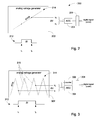
- FIG. 6 an example of an output pulse from pulser 412 in relation to a waveform 442 at the output terminal V out is illustrated.
- four complete segments of the triangular waveform 442 occur, namely segments AB, BC, CD, and DE.
- a “complete segment” may be defined as a segment of the waveform between V High and V Low .
- the voltage level (e.g., v 2 in FIG. 6 ) at the output terminal V out is quantized and loaded into the encoder 408 at a step 512 .
- embodiments of the encoder 408 may be configured to produce a difference between the quantized voltage levels v 1 and v 2 ( FIG. 6 ) obtained in steps 506 and 512 .
- the voltage waveform is cyclic, such as triangular waveform 442 in FIG. 6
- determining the difference between the quantized voltage levels v 1 and v 2 may require “unfolding” the waveform.
- FIG. 7 An example is shown in FIG. 7 , where an unfolded representation 442 ′ of the waveform 442 is illustrated.
- the “difference” between quantized voltage levels v 1 and v 2 amounts to adding together the complete segments (e.g., AB, BC, CD, and DE) and the partial segments 744 a and 744 b .
- Each complete segment e.g., BC
- the voltage difference in the partial segments 744 a and 744 b are computed relative to V High or V Low .
- FIG. 6 shows that the two quantized voltage levels v 1 and v 2 are taken on positive slopes, and hence are referenced to V Low as shown in FIG. 7 .
- the second voltage level is taken on a negative slope (e.g., segment DE), at v 2 ′.
- the output of comparator 432 provides a signal 432 a to the encoder 408 that serves to indicate a state of operation of the voltage generator 402 .
- the signal 432 a indicates whether the slope of the triangular waveform 442 is positive or negative.
- the signal 432 a thus informs the encoder 408 so that a logical unfolding of the triangular waveform 442 is properly performed so that a proper computation can be achieved.
- step 516 the obtained voltage difference ⁇ V is scaled by the slew rate per Eqn. 1 in order to obtain a value for ⁇ t ( FIG. 7 ), the difference in time between the first input signal and the second input signal.
- time to digital conversion processing in accordance with the present disclosure does not require step 516 .
- the process of converting a time value to a digital signal may be considered to be complete with step 514 .
- the digital output of step 514 represents an encoding of the time value, and in some applications that may be sufficient. However, in other applications, step 516 may be performed if the actual time value needs to be digitally represented.
- the capacitor 430 in the relaxation oscillator circuit 402 stores the voltage level of the output terminal V out .
- the voltage level is sampled and held by the capacitor 430 at the end of the pulse from the pulser circuit 412 rather than returning to 0V.
- the relaxation oscillator circuit 402 is enabled upon receiving a subsequent pulse from the pulser circuit 412 , oscillations will start from a voltage level based on the previously sampled voltage stored on the capacitor 430 . In this way, quantization errors resulting from non-linearities in the circuitry (e.g., relaxation oscillator circuit 402 , ADC 404 ) will average out, resulting in first-order quantization noise shaping thus reducing TDC noise.
- This reduced-noise aspect of the TDC 400 is advantageous in a closed loop PLL.
- a TDC 800 may comprise a voltage generator 802 that employs an architecture based on a ring oscillator to generate a cyclic waveform.
- An input section in the voltage generator 802 comprises a pulser circuit 812 that receives a first input signal Sig 1 at time t 1 and a second input signal Sig 2 at time t 2 .
- the pulser circuit 812 generates two pulses P 1 and P 2 .
- the width ⁇ t of the pulses P 1 and P 2 is equal (t 2 ⁇ t 1 ). Pulse P 1 transitions from LO to HI when the first input signal is received, while pulse P 2 transitions from HI to LO.
- pulse P 1 transitions to LO and pulse P 2 transitions to HI.
- the voltage generator further includes a ring oscillator 822 that is enabled and disabled by pulses P 1 and P 2 .
- the ring oscillator 822 comprises a cascade of three inverters; however, higher numbers of cascaded inverters may be employed.
- the pulses P 1 and P 2 control three switches (e.g., CMOS transistors) which connect the respective inverters to first and second voltage potentials (e.g., ground and V cc ).
- Each inverter has an output designated out 1 , out 2 , and out 3 .
- the output out 3 is also an output of the ring oscillator 822 , producing a train of pulses.
- FIG. 9 represents a trace of the output out 3 of a circuit simulation of a 3-stage ring oscillator.
- the voltage generator 802 further includes an extractor circuit 824 . That is connected to the outputs out 1 , out 2 , and out 3 of the inverters of the ring oscillator 822 .
- the extractor circuit 824 comprises three comparators 832 , 834 , and 836 , each comparator receiving a combination of two inverter outputs from the ring oscillator 822 .
- a 3-to-1 mux 838 receives the inverter outputs out 1 , out 2 , and out 3 as mux inputs.
- a mux output is connected to an output terminal 810 of the voltage generator 802 .
- the outputs s 1 , s 2 , and s 3 of the comparators 832 , 834 , and 836 feed into a selector input of the mux 838 .
- An ADC 804 receives the output of one of the inverters of the ring oscillator 822 , as selected by the mux, via the output terminal 810 .
- the ADC 804 quantizes the voltage level at the output terminal and produces a representative digital output signal that feeds into an encoder 808 .
- a counter 806 is connected to the output out 3 of the ring oscillator 822 . The counter counts the pulses in the pulse train.
- the counter 806 outputs a digital count signal that feeds into the encoder 808 .
- the outputs s 1 , s 2 , and s 3 of the comparators 832 , 834 , and 836 feed into the encoder 808 a signal 824 a that indicates a state of operation of the voltage generator 802 .
- FIG. 10 represents a composite waveform 1002 created by superimposing traces of the waveforms at the outputs out 1 , out 2 , and out 3 of the inverters of the ring oscillator 822 . It was discovered that segments of the waveforms at the outputs out 1 , out 2 , and out 3 are sufficiently linear so that a good approximation to a triangular pattern 1004 can be constructed in piecewise fashion.
- the extractor circuit 824 can be configured to generate at the output of its mux, the triangular pattern 1004 by extracting different pieces “a” through “f” of the waveforms at the outputs out 1 , out 2 , and out 3 of the ring oscillator 822 .
- pieces a and d of the triangular pattern 1004 are extracted from the waveform of output out 2 .
- pieces b and e are extracted from the waveform of output out 3
- pieces c and f are extracted from the waveform of output out 1 .
- the multiplexer logic for the mux 838 can be configured to generate the triangular pattern 1004 according to the following: if V out3 >V out2 >V out1 , then output V out2 (piece a) if V out2 >V out3 >V out1 , then output V out3 (piece b) if V out2 >V out1 >V out3 , then output V out1 (piece c) if V out1 >V out2 >V out3 , then output V out2 (piece d) if V out1 >V out3 >V out2 , then output V out3 (piece e) if V out3 >V out1 >V out2 , then output V out1 (piece f), where V out1 , V out2 , and V out3 , are voltage levels of respective outputs out 1 , out 2 , and out 3 .
- the outputs s 1 , s 2 , and s 3 of respective comparators 832 , 834 , and 836 indicate to the encoder 808 whether the sampled voltage is on a positive slope (rising edge) such as piece a ( FIG. 10 ), or on a negative slope (falling edge) such as piece d ( FIG. 10 ).
- the encoder 808 can perform a logical mapping of the triangular to a straight line as explained above in connection with FIG. 7 .
Landscapes
- Physics & Mathematics (AREA)
- General Physics & Mathematics (AREA)
- Engineering & Computer Science (AREA)
- Theoretical Computer Science (AREA)
- Analogue/Digital Conversion (AREA)
Abstract
Description
where
which is orders of magnitude lower than conventional TDCs. In other words, a TDC in accordance with the present disclosure may be able to resolve time differences as low as 32.5 fs.
Even with the significantly reduced performance of the components, the TDC of the present embodiments can still outperform conventional TDC designs. Typical CMOS processes, however, can readily achieve a slew rate of 10 GV/s in the
which is about 100 times better than a conventional gate-delay TDC.
ΔV=(v 2 −v 1). Eqn. 5
ΔV=V segment1 +V segment2 +N×(V High −V Low), Eqn. 6
where:
-
- N is the number of detected complete segments supplied to the
encoder 408 by the counter 406 (for example, inFIG. 6 , N=4), - Vsegment1 represents the voltage difference in
partial segment 744 a, and - Vsegment2 represents the voltage difference in
partial segment 744 b.
In the example shown inFIG. 6 , Vsegment1 is given by (v1−VLow) and Vsegment2=(v2−VLow). It will be apparent that the voltage difference in a partial segment may be referenced to VHigh or VLow, depending on whether the quantized voltage level was sampled on a positive slop of thetriangular waveform 442 or a negative slop of the triangular waveform.
- N is the number of detected complete segments supplied to the
if V out3 >V out2 >V out1, then output V out2 (piece a)
if V out2 >V out3 >V out1, then output V out3 (piece b)
if V out2 >V out1 >V out3, then output V out1 (piece c)
if V out1 >V out2 >V out3, then output V out2 (piece d)
if V out1 >V out3 >V out2, then output V out3 (piece e)
if V out3 >V out1 >V out2, then output V out1 (piece f),
where Vout1, Vout2, and Vout3, are voltage levels of respective outputs out1, out2, and out3.
Claims (19)
Priority Applications (2)
| Application Number | Priority Date | Filing Date | Title |
|---|---|---|---|
| US13/333,058 US8564471B1 (en) | 2011-01-06 | 2011-12-21 | High resolution sampling-based time to digital converter |
| US14/035,307 US8970421B1 (en) | 2011-01-06 | 2013-09-24 | High resolution sampling-based time to digital converter |
Applications Claiming Priority (2)
| Application Number | Priority Date | Filing Date | Title |
|---|---|---|---|
| US201161430407P | 2011-01-06 | 2011-01-06 | |
| US13/333,058 US8564471B1 (en) | 2011-01-06 | 2011-12-21 | High resolution sampling-based time to digital converter |
Related Child Applications (1)
| Application Number | Title | Priority Date | Filing Date |
|---|---|---|---|
| US14/035,307 Continuation US8970421B1 (en) | 2011-01-06 | 2013-09-24 | High resolution sampling-based time to digital converter |
Publications (1)
| Publication Number | Publication Date |
|---|---|
| US8564471B1 true US8564471B1 (en) | 2013-10-22 |
Family
ID=49355245
Family Applications (2)
| Application Number | Title | Priority Date | Filing Date |
|---|---|---|---|
| US13/333,058 Active 2032-01-17 US8564471B1 (en) | 2011-01-06 | 2011-12-21 | High resolution sampling-based time to digital converter |
| US14/035,307 Expired - Fee Related US8970421B1 (en) | 2011-01-06 | 2013-09-24 | High resolution sampling-based time to digital converter |
Family Applications After (1)
| Application Number | Title | Priority Date | Filing Date |
|---|---|---|---|
| US14/035,307 Expired - Fee Related US8970421B1 (en) | 2011-01-06 | 2013-09-24 | High resolution sampling-based time to digital converter |
Country Status (1)
| Country | Link |
|---|---|
| US (2) | US8564471B1 (en) |
Cited By (28)
| Publication number | Priority date | Publication date | Assignee | Title |
|---|---|---|---|---|
| US20130222170A1 (en) * | 2010-06-05 | 2013-08-29 | Dariusz Koscielnik | Method and apparatus for conversion of time interval to digital word |
| US20140152484A1 (en) * | 2011-08-11 | 2014-06-05 | Panasonic Corporation | Oversampling time-to-digital converter |
| US20140240864A1 (en) * | 2013-02-28 | 2014-08-28 | Lsi Corporation | Storage device having degauss circuitry configured for generating degauss signal with asymmetric decay envelopes |
| US20140368372A1 (en) * | 2013-06-14 | 2014-12-18 | Industry-Academic Cooperation Foundation, Yonsei University | Time to digital converter |
| US20150145572A1 (en) * | 2013-11-28 | 2015-05-28 | Megachips Corporation | Time-to-digital converter and pll circuit using the same |
| US9081370B2 (en) * | 2012-02-29 | 2015-07-14 | Panasonic Intellectual Property Management Co., Ltd. | Time-to-digital converter and an A/D converter including the same |
| US20150212128A1 (en) * | 2014-01-29 | 2015-07-30 | Taiwan Semiconductor Manufacturing Co. Limited | Rise time and fall time measurement |
| US20160156434A1 (en) * | 2013-07-31 | 2016-06-02 | Kuang-Chi Intelligent Photonic Technology Ltd. | Error retransmission mechanism-comprised methods, apparatuses and systems for transmitting and receiving visible light signal |
| US9746832B1 (en) | 2016-09-09 | 2017-08-29 | Samsung Electronics Co., Ltd | System and method for time-to-digital converter fine-conversion using analog-to-digital converter (ADC) |
| US9923574B2 (en) * | 2014-11-04 | 2018-03-20 | Cirrus Logic, Inc. | Analogue-to-digital converter |
| US10067478B1 (en) * | 2017-12-11 | 2018-09-04 | Silicon Laboratories Inc. | Use of a recirculating delay line with a time-to-digital converter |
| US10171101B1 (en) * | 2017-12-20 | 2019-01-01 | Cirrus Logic, Inc. | Modulators |
| CN109245765A (en) * | 2018-06-29 | 2019-01-18 | 西安电子科技大学昆山创新研究院 | TDC_ADC multiplexing technology |
| US20190187628A1 (en) * | 2017-12-20 | 2019-06-20 | Integrated Device Technology, Inc. | Use of ring oscillators for multi-stop time measurements |
| US10574256B1 (en) * | 2018-09-25 | 2020-02-25 | Cirrus Logic, Inc. | Modulators |
| US10819363B2 (en) | 2018-09-25 | 2020-10-27 | Cirrus Logic, Inc. | Modulators |
| US10826514B1 (en) * | 2019-10-15 | 2020-11-03 | Ciena Corporation | Noise-shaping enhanced gated ring oscillator based analog-to-digital converters |
| US20200412376A1 (en) * | 2019-06-26 | 2020-12-31 | Intel Corporation | Ring oscillator-based analog-to-digital converter |
| WO2021101741A1 (en) | 2019-11-19 | 2021-05-27 | Texas Instruments Incorporated | Storage cell ring-based time-to-digital converter |
| US20220067492A1 (en) * | 2020-08-31 | 2022-03-03 | National Tsing Hua University | Neuromorphic system and methodology for switching between functional operations |
| US11320792B2 (en) * | 2019-08-07 | 2022-05-03 | Seiko Epson Corporation | Circuit device, physical quantity measuring device, electronic apparatus, and vehicle |
| US20220216877A1 (en) * | 2021-01-07 | 2022-07-07 | AyDeeKay LLC dba Indie Semiconductor | Digitally Calibrated Programmable Clock Phase Generation Circuit |
| US20230053266A1 (en) * | 2021-01-27 | 2023-02-16 | Zhejiang University | Low-power fractional-n phase-locked loop circuit |
| CN116208158A (en) * | 2023-03-08 | 2023-06-02 | 中北大学 | TDC-based multi-voltage threshold sampling method, system and equipment |
| US20240007123A1 (en) * | 2022-06-29 | 2024-01-04 | Rohde & Schwarz Gmbh & Co. Kg | Multipath d/a converter |
| US20240072815A1 (en) * | 2022-08-30 | 2024-02-29 | Apple Inc. | Digital-to-analog converter with localized frequency multiplication circuits |
| US20240219867A1 (en) * | 2021-03-02 | 2024-07-04 | Anokiwave, Inc. | Time-to-digital converter using voltage as a representation of time offset |
| CN120263148A (en) * | 2025-06-05 | 2025-07-04 | 湖南融创微电子股份有限公司 | Three-mode radiation-resistant clock circuit |
Families Citing this family (8)
| Publication number | Priority date | Publication date | Assignee | Title |
|---|---|---|---|---|
| US9213316B2 (en) * | 2014-02-06 | 2015-12-15 | Texas Instruments Incorporated | Circuit for detecting and correcting timing errors |
| US9529336B2 (en) * | 2015-02-25 | 2016-12-27 | Taiwan Semiconductor Manufacturing Company, Ltd. | Analog to digital converter compatible with image sensor readout |
| EP3096461B1 (en) * | 2015-05-21 | 2020-08-05 | AKADEMIA GORNICZO-HUTNICZA im. Stanislawa Staszica | Method and apparatus for encoding analog signal into time intervals |
| US9568889B1 (en) * | 2016-06-15 | 2017-02-14 | Winbond Electronics Corp. | Time to digital converter with high resolution |
| US10879922B2 (en) * | 2018-08-16 | 2020-12-29 | Microchip Technology Incorporated | Time-based, current-controlled paired oscillator analog-to-digital converter with selectable resolution |
| WO2020113360A1 (en) * | 2018-12-03 | 2020-06-11 | 深圳市大疆创新科技有限公司 | Sampling circuit, sampling method, ranging apparatus and mobile platform |
| US10895850B1 (en) | 2019-07-25 | 2021-01-19 | Si-Ware Systems S.A.E. | Mixed-domain circuit with differential domain-converters |
| US12603652B1 (en) * | 2023-11-22 | 2026-04-14 | Hrl Laboratories, Llc | Scalable architecture for synchronized arbitrary waveforms |
Citations (1)
| Publication number | Priority date | Publication date | Assignee | Title |
|---|---|---|---|---|
| US7609756B2 (en) * | 2005-12-27 | 2009-10-27 | Multigig Inc. | Rotary clock flash analog to digital converter system and method |
Family Cites Families (1)
| Publication number | Priority date | Publication date | Assignee | Title |
|---|---|---|---|---|
| US7741917B2 (en) * | 2008-11-07 | 2010-06-22 | Telefonaktiebolaget Lm Ericsson (Publ) | Noise shaping time to digital converter |
-
2011
- 2011-12-21 US US13/333,058 patent/US8564471B1/en active Active
-
2013
- 2013-09-24 US US14/035,307 patent/US8970421B1/en not_active Expired - Fee Related
Patent Citations (1)
| Publication number | Priority date | Publication date | Assignee | Title |
|---|---|---|---|---|
| US7609756B2 (en) * | 2005-12-27 | 2009-10-27 | Multigig Inc. | Rotary clock flash analog to digital converter system and method |
Non-Patent Citations (5)
| Title |
|---|
| C.-M. Hsu, M.Z. Straayer, and M.H. Perrott, "A Low-Noise, Wide-Bw 3.6GHz Digital Fractional-N SigmaDeltaFrequency Synthesizer with a Noise-Shaping Time-to-Digital Converter and Quantization Noise Cancellation," ISSCC Dig. Tech. Papers, pp. 340-341, Feb., 2008. |
| C.-M. Hsu, M.Z. Straayer, and M.H. Perrott, "A Low-Noise, Wide-Bw 3.6GHz Digital Fractional-N ΣΔFrequency Synthesizer with a Noise-Shaping Time-to-Digital Converter and Quantization Noise Cancellation," ISSCC Dig. Tech. Papers, pp. 340-341, Feb., 2008. |
| M. Straayer and M. Perrott, "An efficient high-resolution 11-bit noise shaping multipath gated ring oscillator TDC," in VLSI Symp. Dig. Tech. Papers, pp. 82-83, Jun. 2008. |
| N. Da Dalt, E. Thaller, P. Gregorius, et al., "A Compact Triple-Band Low-Jitter Digital LC PLL with Programmable Coil in 130-nm CMOS," IEEE J. Solid-State Circuits, vol. 40, No. 7, pp. 1482-1490, Jul. 2005. |
| R. B. Staszewski, J.L. Wallberg, S. Rezeq, et al., "All-Digital PLL and Transmitter for Mobile Phones," IEEE J. Solid-State Circuits, vol. 40, No. 12, pp. 2469-2482, Dec., 2005. |
Cited By (57)
| Publication number | Priority date | Publication date | Assignee | Title |
|---|---|---|---|---|
| US9063518B2 (en) * | 2010-06-05 | 2015-06-23 | Akademia Gorniczo-Hutnicza Im. Stanislawa Staszica, Al. | Method and apparatus for conversion of time interval to digital word |
| US20130222170A1 (en) * | 2010-06-05 | 2013-08-29 | Dariusz Koscielnik | Method and apparatus for conversion of time interval to digital word |
| US20140152484A1 (en) * | 2011-08-11 | 2014-06-05 | Panasonic Corporation | Oversampling time-to-digital converter |
| US9024793B2 (en) * | 2011-08-11 | 2015-05-05 | Panasonic Intellectual Property Management Co., Ltd. | Oversampling time-to-digital converter |
| US9081370B2 (en) * | 2012-02-29 | 2015-07-14 | Panasonic Intellectual Property Management Co., Ltd. | Time-to-digital converter and an A/D converter including the same |
| US20140240864A1 (en) * | 2013-02-28 | 2014-08-28 | Lsi Corporation | Storage device having degauss circuitry configured for generating degauss signal with asymmetric decay envelopes |
| US8873188B2 (en) * | 2013-02-28 | 2014-10-28 | Lsi Corporation | Storage device having degauss circuitry configured for generating degauss signal with asymmetric decay envelopes |
| US20140368372A1 (en) * | 2013-06-14 | 2014-12-18 | Industry-Academic Cooperation Foundation, Yonsei University | Time to digital converter |
| US9124280B2 (en) * | 2013-06-14 | 2015-09-01 | Industry-Academic Cooperation Foundation, Yonsei University | Time to digital converter |
| US20160156434A1 (en) * | 2013-07-31 | 2016-06-02 | Kuang-Chi Intelligent Photonic Technology Ltd. | Error retransmission mechanism-comprised methods, apparatuses and systems for transmitting and receiving visible light signal |
| US10116420B2 (en) * | 2013-07-31 | 2018-10-30 | Kuang-Chi Intelligent Photonic Technology Ltd. | Error retransmission mechanism-comprised methods, apparatuses and systems for transmitting and receiving visible light signal |
| US20150145572A1 (en) * | 2013-11-28 | 2015-05-28 | Megachips Corporation | Time-to-digital converter and pll circuit using the same |
| US9170564B2 (en) * | 2013-11-28 | 2015-10-27 | Megachips Corporation | Time-to-digital converter and PLL circuit using the same |
| US20150212128A1 (en) * | 2014-01-29 | 2015-07-30 | Taiwan Semiconductor Manufacturing Co. Limited | Rise time and fall time measurement |
| US9519015B2 (en) * | 2014-01-29 | 2016-12-13 | Taiwan Semiconductor Manufacturing Company Limited | Rise time and fall time measurement |
| US9923574B2 (en) * | 2014-11-04 | 2018-03-20 | Cirrus Logic, Inc. | Analogue-to-digital converter |
| US9746832B1 (en) | 2016-09-09 | 2017-08-29 | Samsung Electronics Co., Ltd | System and method for time-to-digital converter fine-conversion using analog-to-digital converter (ADC) |
| US10067478B1 (en) * | 2017-12-11 | 2018-09-04 | Silicon Laboratories Inc. | Use of a recirculating delay line with a time-to-digital converter |
| USRE48735E1 (en) * | 2017-12-11 | 2021-09-14 | Silicon Laboratories Inc. | Use of a recirculating delay line with a time-to-digital converter |
| US10171101B1 (en) * | 2017-12-20 | 2019-01-01 | Cirrus Logic, Inc. | Modulators |
| US20190190532A1 (en) * | 2017-12-20 | 2019-06-20 | Cirrus Logic International Semiconductor Ltd. | Modulators |
| US20190187628A1 (en) * | 2017-12-20 | 2019-06-20 | Integrated Device Technology, Inc. | Use of ring oscillators for multi-stop time measurements |
| US10534322B2 (en) * | 2017-12-20 | 2020-01-14 | Integrated Device Technology, Inc. | Use of ring oscillators for multi-stop time measurements |
| US10651868B2 (en) * | 2017-12-20 | 2020-05-12 | Cirrus Logic, Inc. | Modulators |
| CN109245765A (en) * | 2018-06-29 | 2019-01-18 | 西安电子科技大学昆山创新研究院 | TDC_ADC multiplexing technology |
| CN109245765B (en) * | 2018-06-29 | 2022-06-07 | 西安电子科技大学昆山创新研究院 | TDC _ ADC multiplexing techniques |
| US10574256B1 (en) * | 2018-09-25 | 2020-02-25 | Cirrus Logic, Inc. | Modulators |
| US10819363B2 (en) | 2018-09-25 | 2020-10-27 | Cirrus Logic, Inc. | Modulators |
| US11165436B2 (en) | 2018-09-25 | 2021-11-02 | Cirrus Logic, Inc. | Modulators |
| US11038523B2 (en) * | 2019-06-26 | 2021-06-15 | Intel Corporation | Ring oscillator-based analog-to-digital converter |
| US20200412376A1 (en) * | 2019-06-26 | 2020-12-31 | Intel Corporation | Ring oscillator-based analog-to-digital converter |
| US11320792B2 (en) * | 2019-08-07 | 2022-05-03 | Seiko Epson Corporation | Circuit device, physical quantity measuring device, electronic apparatus, and vehicle |
| US10826514B1 (en) * | 2019-10-15 | 2020-11-03 | Ciena Corporation | Noise-shaping enhanced gated ring oscillator based analog-to-digital converters |
| US11770126B2 (en) | 2019-10-15 | 2023-09-26 | Ciena Corporation | Noise-shaping enhanced gated ring oscillator based analog-to-digital converters |
| CN114787927A (en) * | 2019-11-19 | 2022-07-22 | 德州仪器公司 | Time-to-digital converter based on storage unit ring |
| CN114787927B (en) * | 2019-11-19 | 2025-05-13 | 德州仪器公司 | Time-to-digital converter based on memory cell ring |
| WO2021101741A1 (en) | 2019-11-19 | 2021-05-27 | Texas Instruments Incorporated | Storage cell ring-based time-to-digital converter |
| EP4062409A4 (en) * | 2019-11-19 | 2023-01-04 | Texas Instruments Incorporated | RING-BASED TIME-TO-DIGITAL CONVERTER OF A MEMORY CELL |
| US12079709B2 (en) * | 2020-08-31 | 2024-09-03 | National Tsing Hua University | Neuromorphic system and methodology for switching between functional operations |
| US20220067492A1 (en) * | 2020-08-31 | 2022-03-03 | National Tsing Hua University | Neuromorphic system and methodology for switching between functional operations |
| US11831322B2 (en) * | 2021-01-07 | 2023-11-28 | AyDeeKay LLC | Digitally calibrated programmable clock phase generation circuit |
| US20230238968A1 (en) * | 2021-01-07 | 2023-07-27 | AyDeeKay LLC dba Indie Semiconductor | Digitally Calibrated Programmable Clock Phase Generation Circuit |
| US11641206B2 (en) * | 2021-01-07 | 2023-05-02 | AyDeeKay LLC | Digitally calibrated programmable clock phase generation circuit |
| US12136924B2 (en) * | 2021-01-07 | 2024-11-05 | AyDeeKay LLC | Digitally calibrated programmable clock phase generation circuit |
| US20240030925A1 (en) * | 2021-01-07 | 2024-01-25 | AyDeeKay LLC dba Indie Semiconductor | Digitally Calibrated Programmable Clock Phase Generation Circuit |
| US20250030425A1 (en) * | 2021-01-07 | 2025-01-23 | AyDeeKay LLC dba Indie Semiconductor | Digitally Calibrated Programmable Clock Phase Generation Circuit |
| US20220216877A1 (en) * | 2021-01-07 | 2022-07-07 | AyDeeKay LLC dba Indie Semiconductor | Digitally Calibrated Programmable Clock Phase Generation Circuit |
| US11936390B2 (en) * | 2021-01-27 | 2024-03-19 | Zhejiang University | Low-power fractional-N phase-locked loop circuit |
| US20230053266A1 (en) * | 2021-01-27 | 2023-02-16 | Zhejiang University | Low-power fractional-n phase-locked loop circuit |
| US12292716B2 (en) * | 2021-03-02 | 2025-05-06 | Anokiwave, Inc. | Time-to-digital converter using voltage as a representation of time offset |
| US20240219867A1 (en) * | 2021-03-02 | 2024-07-04 | Anokiwave, Inc. | Time-to-digital converter using voltage as a representation of time offset |
| US12088319B2 (en) * | 2022-06-29 | 2024-09-10 | Rohde & Schwarz Gmbh & Co. Kg | Multipath D/A converter |
| US20240007123A1 (en) * | 2022-06-29 | 2024-01-04 | Rohde & Schwarz Gmbh & Co. Kg | Multipath d/a converter |
| US12166495B2 (en) * | 2022-08-30 | 2024-12-10 | Apple Inc. | Digital-to-analog converter with localized frequency multiplication circuits |
| US20240072815A1 (en) * | 2022-08-30 | 2024-02-29 | Apple Inc. | Digital-to-analog converter with localized frequency multiplication circuits |
| CN116208158A (en) * | 2023-03-08 | 2023-06-02 | 中北大学 | TDC-based multi-voltage threshold sampling method, system and equipment |
| CN120263148A (en) * | 2025-06-05 | 2025-07-04 | 湖南融创微电子股份有限公司 | Three-mode radiation-resistant clock circuit |
Also Published As
| Publication number | Publication date |
|---|---|
| US8970421B1 (en) | 2015-03-03 |
Similar Documents
| Publication | Publication Date | Title |
|---|---|---|
| US8564471B1 (en) | High resolution sampling-based time to digital converter | |
| Mattada et al. | Time‐to‐digital converters—A comprehensive review | |
| CN102334038B (en) | Phase Measuring Device, and Frequency Measuring Device | |
| US9746832B1 (en) | System and method for time-to-digital converter fine-conversion using analog-to-digital converter (ADC) | |
| US11664813B2 (en) | Delay circuit, time to digital converter, and A/D conversion circuit | |
| US12191879B2 (en) | Receiver | |
| Delagnes et al. | The SAMPIC waveform and time to digital converter | |
| Park et al. | A single-slope 80MS/s ADC using two-step time-to-digital conversion | |
| CN103297039A (en) | Digital phase-locked loop device and method | |
| US10972116B2 (en) | Time to digital converter and A/D conversion circuit | |
| Nguyen et al. | A 4.7-ps resolution recirculating cyclic Vernier TDC using DWA-based mismatch correction and a register-based time amplifier | |
| US9379879B1 (en) | Noise-shaping time-to-digital converter | |
| US6950375B2 (en) | Multi-phase clock time stamping | |
| US11075621B2 (en) | Delay circuit, time to digital converter, and A/D conversion circuit | |
| US11121717B2 (en) | A/D conversion circuit | |
| US10528010B2 (en) | Range finding device | |
| Wu et al. | A 9-bit 215-MS/s folding-flash time-to-digital converter based on redundant remainder number system | |
| Vornicu et al. | Wide range 8ps incremental resolution time interval generator based on FPGA technology | |
| Deng et al. | A high-precision coarse-fine time-to-digital converter with the analog-digital hybrid interpolation | |
| JP2023165583A (en) | Correction system for eliminating phase noise effects and analog-to-digital converter including it | |
| CN113346879A (en) | Annular carry chain TDC circuit based on fine delay phase shift and measurement method thereof | |
| Uemori et al. | Multi-bit sigma-delta TDC architecture with self-calibration | |
| Arakawa et al. | Linearity improvement technique of multi-bit sigma-delta TDC for timing measurement | |
| Huang et al. | A new cycle-time-to-digital converter with two level conversion scheme | |
| Lee | A low power two-step cyclic time-to-digital converter without startup time error in 180 nm CMOS |
Legal Events
| Date | Code | Title | Description |
|---|---|---|---|
| AS | Assignment |
Owner name: MARVELL INTERNATIONAL LTD., BERMUDA Free format text: ASSIGNMENT OF ASSIGNORS INTEREST;ASSIGNOR:MARVELL SEMICONDUCTOR, INC.;REEL/FRAME:027434/0548 Effective date: 20111221 Owner name: MARVELL SEMICONDUCTOR, INC., CALIFORNIA Free format text: ASSIGNMENT OF ASSIGNORS INTEREST;ASSIGNORS:GAO, XIANG;YAO, CHIH-WEI;LIN, CHI-HUNG;AND OTHERS;REEL/FRAME:027434/0527 Effective date: 20111220 |
|
| STCF | Information on status: patent grant |
Free format text: PATENTED CASE |
|
| FPAY | Fee payment |
Year of fee payment: 4 |
|
| AS | Assignment |
Owner name: CAVIUM INTERNATIONAL, CAYMAN ISLANDS Free format text: ASSIGNMENT OF ASSIGNORS INTEREST;ASSIGNOR:MARVELL INTERNATIONAL LTD.;REEL/FRAME:052918/0001 Effective date: 20191231 |
|
| AS | Assignment |
Owner name: MARVELL ASIA PTE, LTD., SINGAPORE Free format text: ASSIGNMENT OF ASSIGNORS INTEREST;ASSIGNOR:CAVIUM INTERNATIONAL;REEL/FRAME:053475/0001 Effective date: 20191231 |
|
| MAFP | Maintenance fee payment |
Free format text: PAYMENT OF MAINTENANCE FEE, 8TH YEAR, LARGE ENTITY (ORIGINAL EVENT CODE: M1552); ENTITY STATUS OF PATENT OWNER: LARGE ENTITY Year of fee payment: 8 |
|
| MAFP | Maintenance fee payment |
Free format text: PAYMENT OF MAINTENANCE FEE, 12TH YEAR, LARGE ENTITY (ORIGINAL EVENT CODE: M1553); ENTITY STATUS OF PATENT OWNER: LARGE ENTITY Year of fee payment: 12 |