US8564155B2 - Multiple output power supply - Google Patents
Multiple output power supply Download PDFInfo
- Publication number
- US8564155B2 US8564155B2 US12/800,094 US80009410A US8564155B2 US 8564155 B2 US8564155 B2 US 8564155B2 US 80009410 A US80009410 A US 80009410A US 8564155 B2 US8564155 B2 US 8564155B2
- Authority
- US
- United States
- Prior art keywords
- channel
- current
- storage element
- energy
- output
- Prior art date
- Legal status (The legal status is an assumption and is not a legal conclusion. Google has not performed a legal analysis and makes no representation as to the accuracy of the status listed.)
- Active, expires
Links
Images


Classifications
-
- H—ELECTRICITY
- H02—GENERATION; CONVERSION OR DISTRIBUTION OF ELECTRIC POWER
- H02M—APPARATUS FOR CONVERSION BETWEEN AC AND AC, BETWEEN AC AND DC, OR BETWEEN DC AND DC, AND FOR USE WITH MAINS OR SIMILAR POWER SUPPLY SYSTEMS; CONVERSION OF DC OR AC INPUT POWER INTO SURGE OUTPUT POWER; CONTROL OR REGULATION THEREOF
- H02M3/00—Conversion of DC power input into DC power output
- H02M3/02—Conversion of DC power input into DC power output without intermediate conversion into AC
- H02M3/04—Conversion of DC power input into DC power output without intermediate conversion into AC by static converters
- H02M3/10—Conversion of DC power input into DC power output without intermediate conversion into AC by static converters using discharge tubes with control electrode or semiconductor devices with control electrode
- H02M3/145—Conversion of DC power input into DC power output without intermediate conversion into AC by static converters using discharge tubes with control electrode or semiconductor devices with control electrode using devices of a triode or transistor type requiring continuous application of a control signal
- H02M3/155—Conversion of DC power input into DC power output without intermediate conversion into AC by static converters using discharge tubes with control electrode or semiconductor devices with control electrode using devices of a triode or transistor type requiring continuous application of a control signal using semiconductor devices only
- H02M3/156—Conversion of DC power input into DC power output without intermediate conversion into AC by static converters using discharge tubes with control electrode or semiconductor devices with control electrode using devices of a triode or transistor type requiring continuous application of a control signal using semiconductor devices only with automatic control of output voltage or current, e.g. switching regulators
- H02M3/158—Conversion of DC power input into DC power output without intermediate conversion into AC by static converters using discharge tubes with control electrode or semiconductor devices with control electrode using devices of a triode or transistor type requiring continuous application of a control signal using semiconductor devices only with automatic control of output voltage or current, e.g. switching regulators including plural semiconductor devices as final control devices for a single load
-
- H—ELECTRICITY
- H05—ELECTRIC TECHNIQUES NOT OTHERWISE PROVIDED FOR
- H05B—ELECTRIC HEATING; ELECTRIC LIGHT SOURCES NOT OTHERWISE PROVIDED FOR; CIRCUIT ARRANGEMENTS FOR ELECTRIC LIGHT SOURCES, IN GENERAL
- H05B45/00—Circuit arrangements for operating light-emitting diodes [LED]
- H05B45/30—Driver circuits
- H05B45/32—Pulse-control circuits
- H05B45/327—Burst dimming
-
- H—ELECTRICITY
- H05—ELECTRIC TECHNIQUES NOT OTHERWISE PROVIDED FOR
- H05B—ELECTRIC HEATING; ELECTRIC LIGHT SOURCES NOT OTHERWISE PROVIDED FOR; CIRCUIT ARRANGEMENTS FOR ELECTRIC LIGHT SOURCES, IN GENERAL
- H05B45/00—Circuit arrangements for operating light-emitting diodes [LED]
- H05B45/30—Driver circuits
- H05B45/37—Converter circuits
- H05B45/3725—Switched mode power supply [SMPS]
- H05B45/375—Switched mode power supply [SMPS] using buck topology
-
- H—ELECTRICITY
- H05—ELECTRIC TECHNIQUES NOT OTHERWISE PROVIDED FOR
- H05B—ELECTRIC HEATING; ELECTRIC LIGHT SOURCES NOT OTHERWISE PROVIDED FOR; CIRCUIT ARRANGEMENTS FOR ELECTRIC LIGHT SOURCES, IN GENERAL
- H05B45/00—Circuit arrangements for operating light-emitting diodes [LED]
- H05B45/30—Driver circuits
- H05B45/37—Converter circuits
- H05B45/3725—Switched mode power supply [SMPS]
- H05B45/38—Switched mode power supply [SMPS] using boost topology
-
- H—ELECTRICITY
- H05—ELECTRIC TECHNIQUES NOT OTHERWISE PROVIDED FOR
- H05B—ELECTRIC HEATING; ELECTRIC LIGHT SOURCES NOT OTHERWISE PROVIDED FOR; CIRCUIT ARRANGEMENTS FOR ELECTRIC LIGHT SOURCES, IN GENERAL
- H05B45/00—Circuit arrangements for operating light-emitting diodes [LED]
- H05B45/30—Driver circuits
- H05B45/37—Converter circuits
- H05B45/3725—Switched mode power supply [SMPS]
- H05B45/382—Switched mode power supply [SMPS] with galvanic isolation between input and output
-
- H—ELECTRICITY
- H05—ELECTRIC TECHNIQUES NOT OTHERWISE PROVIDED FOR
- H05B—ELECTRIC HEATING; ELECTRIC LIGHT SOURCES NOT OTHERWISE PROVIDED FOR; CIRCUIT ARRANGEMENTS FOR ELECTRIC LIGHT SOURCES, IN GENERAL
- H05B45/00—Circuit arrangements for operating light-emitting diodes [LED]
- H05B45/30—Driver circuits
- H05B45/37—Converter circuits
- H05B45/3725—Switched mode power supply [SMPS]
- H05B45/385—Switched mode power supply [SMPS] using flyback topology
-
- H—ELECTRICITY
- H05—ELECTRIC TECHNIQUES NOT OTHERWISE PROVIDED FOR
- H05B—ELECTRIC HEATING; ELECTRIC LIGHT SOURCES NOT OTHERWISE PROVIDED FOR; CIRCUIT ARRANGEMENTS FOR ELECTRIC LIGHT SOURCES, IN GENERAL
- H05B45/00—Circuit arrangements for operating light-emitting diodes [LED]
- H05B45/30—Driver circuits
- H05B45/37—Converter circuits
- H05B45/3725—Switched mode power supply [SMPS]
- H05B45/39—Circuits containing inverter bridges
-
- H—ELECTRICITY
- H05—ELECTRIC TECHNIQUES NOT OTHERWISE PROVIDED FOR
- H05B—ELECTRIC HEATING; ELECTRIC LIGHT SOURCES NOT OTHERWISE PROVIDED FOR; CIRCUIT ARRANGEMENTS FOR ELECTRIC LIGHT SOURCES, IN GENERAL
- H05B45/00—Circuit arrangements for operating light-emitting diodes [LED]
- H05B45/40—Details of LED load circuits
- H05B45/44—Details of LED load circuits with an active control inside an LED matrix
- H05B45/46—Details of LED load circuits with an active control inside an LED matrix having LEDs disposed in parallel lines
-
- H—ELECTRICITY
- H02—GENERATION; CONVERSION OR DISTRIBUTION OF ELECTRIC POWER
- H02M—APPARATUS FOR CONVERSION BETWEEN AC AND AC, BETWEEN AC AND DC, OR BETWEEN DC AND DC, AND FOR USE WITH MAINS OR SIMILAR POWER SUPPLY SYSTEMS; CONVERSION OF DC OR AC INPUT POWER INTO SURGE OUTPUT POWER; CONTROL OR REGULATION THEREOF
- H02M1/00—Details of apparatus for conversion
- H02M1/0083—Converters characterised by their input or output configuration
- H02M1/009—Converters characterised by their input or output configuration having two or more independently controlled outputs
Definitions
- the reduction in size of electronic devices creates a need to minimize off chip circuitry components to reduce component cost and required board size.
- One of the larger elements typically required in a power supply for electronic devices is an inductor.
- an inductor When a device has multiple loads which have different power requirements, there are two typical options: use multiple power drivers which require multiple inductors, or find a way to use a single inductor for multiple loads.
- SIMO power supplies have been developed to meet the needs of multiple voltage based loads.
- a SIMO supply may have a 1.6V, 3.3V, and 5V output driven from a single inductor. Not all loads, however, are voltage dependent.
- An example of this is a string of light emitting diodes (LEDs).
- An LED is a current based device which can have a different forward voltage from device to device.
- a voltage regulated power supply is less than ideal for this type of load. Dimming LEDs generally requires the current supply to be rapidly turned on and off using a pulse width modulation technique. It would be desirable to have a multiple output power supply which could regulate a variety of load types and dim the outputs by pulse width modulation.
- One aspect of the invention provides a method for supplying power to multiple output channels.
- Channel control signals are monitored to determine a state for each of the output channels.
- Each channel control signal is associated with one of the output channels.
- the energy in a storage element is directed to the output channels according to the state of the channel control signals.
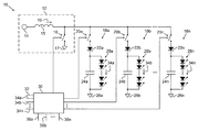
- FIG. 1 is a circuit schematic of a boost mode single inductor multiple output (SIMO) power supply.
- SIMO boost mode single inductor multiple output
- FIG. 2 is a circuit schematic of a boost mode SIMO power supply showing an alternate switch configuration.
- FIG. 3 is a circuit schematic of a boost mode SIMO power supply including a freewheel switch.
- FIG. 4 is a circuit schematic of a boost mode SIMO power supply showing an alternate freewheel switch configuration.
- FIG. 5 is a circuit schematic of a flyback SIMO power supply including a freewheel switch.
- FIG. 6 is a circuit schematic of a forward converter SIMO power supply including a freewheel switch.
- FIG. 7 is a circuit schematic of a buck converter SIMO power supply.
- FIG. 8 is a circuit schematic of a buck-boost SIMO power supply.
- FIG. 9 is a circuit schematic of a forward converter SIMO power supply including a freewheel switch.
- FIG. 10 is a circuit schematic of a SEPIC converter SIMO power supply.
- FIG. 11 is a circuit schematic of a boost mode multiple inductor multiple output power supply.
- FIG. 12 is a timing diagram illustrating output current regulation.
- FIG. 13 a is a timing diagram illustrating dimming control utilizing current regulation and pulse width modulation at a 75% duty cycle.
- FIG. 13 b is a timing diagram illustrating dimming control utilizing current regulation and pulse width modulation at a 50% duty cycle.
- FIG. 14 is a timing diagram illustrating dimming control using a analog dimming method.
- FIG. 15 is a timing diagram illustrating dimming utilizing CCM control without a freewheel switch.
- FIG. 16 is a timing diagram illustrating the DCM “alternating method.”
- FIG. 17 is a timing diagram illustrating the DCM “alternating method” with a buck topology circuit.
- FIG. 18 is a timing diagram illustrating the DCM “skip channel alternating method.”
- FIG. 19 is a timing diagram illustrating the DCM “multiplexing method.”
- FIG. 20 is a timing diagram illustrating dimming utilizing the CCM “alternating method” and a freewheel switch.
- FIG. 21 is a timing diagram illustrating dimming utilizing the CCM “multiplexing method” and a freewheel switch.
- SIMO singe inductor multiple output
- a SIMO power supply In the case of voltage regulated loads, a SIMO power supply must respond to a transient current at the load with good cross regulation characteristics.
- Cross regulation is the error in voltage regulation on a channel that has a static load current when a different channel has had a change in its load current.
- An additional and desirable feature for LEDs is dimming functionality which can be achieved using methods such as pulse width modulation (PWM) or by modulating the regulation point.
- PWM pulse width modulation
- the SIMO power supply must be capable of independently turning on and off (enabling and disabling) channels to pulse width modulate the LEDs or to modulate the regulation point in response to control inputs.
- One embodiment of the present invention is a boost mode SIMO power supply which is illustrated in FIG. 1 as circuit 10 .
- Current supply subcomponent 12 has voltage input 14 connected to inductor 15 , and includes main switch 16 to ground contact 17 which stores energy in inductor 15 .
- Current supply subcomponent 12 is connected in parallel with a plurality of output channels 18 a - 18 n .
- Each output channel 18 a - 18 n has corresponding channel switch 20 a - 20 n connected in series with diodes 22 a - 22 n , the parallel combination of capacitors 24 a - 24 n and loads 28 a - 28 n , and ground contacts 26 a - 26 n .
- Diodes 22 a - 22 n may not be required if channel switches 20 a - 20 n can block both positive and negative potentials. Diodes may also not be required on every output channel, particularly the channel with the lowest potential since the channel switch will never see a negative potential.
- Loads 28 a - 28 n in this case a plurality of LEDs, are connected in parallel with capacitors 24 a - 24 n to sustain a DC current through loads 28 a - 28 n while energy is not being delivered by current supply subcomponent 12 .
- Output channels 18 a - 18 n are individually activated by channel switches 20 a - 20 n to multiplex the energy delivered by current supply subcomponent 12 .
- Switches 16 and 20 a - 20 n are controlled by controller 30 which also monitors inductor current 32 and load currents 34 a - n , and responds to channel enable inputs 36 a - n to enable PWM dimming of the LED loads.
- FIG. 2 shows circuit 50 , another possible embodiment of a boost mode topology SIMO similar to that shown in FIG. 1 with an alternate switch configuration.
- Current supply subcomponent 51 is the same boost mode configuration as current supply subcomponent 12 of FIG. 1 .
- circuit 50 has channel switches 52 a - 52 n adjacent to ground contacts 54 a - 54 n rather than inductor 56 .
- a variety of switch locations are suitable and all switches are operated by controller 58 .
- FIG. 3 illustrates another possible embodiment with circuit 100 utilizing a boost mode power supply that includes a freewheel switch.
- Current supply subcomponent 101 with voltage input 102 and inductor 104 has the same boost mode configuration as current supply subcomponent 12 of FIG. 1 .
- an output channel without a load has been added to circuit 100 .
- This additional output channel connects the output of current supply subcomponent 101 back to voltage input 102 through freewheel switch 106 .
- the remainder of the circuit (with the exception of an additional output from controller 112 to operate freewheel switch 106 ), is the same as that described with respect to FIG. 2 .
- FIG. 4 illustrates an alternative implementation of a freewheel switch with circuit 150 that includes an extra output channel to provide the freewheel function.
- Current supply subcomponent 151 has voltage input 152 connected to inductor 154 in a boost mode configuration the same as that described with respect to FIG. 1 .
- the other terminal of inductor 154 is connected to the parallel combination of main switch 156 to ground contact 158 , resistor 160 to freewheel switch 162 to ground contact 164 , and output channels 166 a - 166 n .
- Freewheel switch 162 maintains the current in inductor 154 by forcing the voltage across inductor 154 close to zero with the voltage drop across resistor 160 .
- This accomplishes the same basic idea of the freewheel circuit shown in FIG. 3 that accommodates inductor current without discharging into an output channel. The difference is that inductor charge is likely not to be maintained, instead it is slowly reduced or increased through the extra output channel.
- the circuit is operated by controller 168 .
- FIG. 5 illustrates an alternate embodiment using a flyback power supply shown as circuit 250 .
- Current supply subcomponent 251 has voltage input 252 connected with one side of coupled inductor 254 in series with main switch 256 and ground 258 . The other side of coupled inductor 254 is connected with ground contact 260 .
- This configuration is known as a flyback power supply.
- the output of current supply subcomponent 251 is connected to freewheel switch 262 to ground contact 264 and a plurality of output channels 266 a - 266 n . Since the output of coupled inductor 254 is ground referenced, a zero voltage across the inductor is achieved with ground referenced freewheel switch 262 .
- the freewheel switch is not required for all modes of operation and can be removed from circuit 250 in those cases.
- the circuit is operated by controller 268 .
- FIG. 6 illustrates another possible embodiment utilizing a forward converter power supply in circuit 300 .
- Current supply subcomponent 301 has voltage input 302 that is connected to two parallel legs.
- the first includes first main switch 304 a and reverse biased diode 306 to ground contact 308 .
- the second includes diode 310 and second main switch 304 b to ground contact 312 .
- the terminals of the first side of transformer 314 are connected between first main switch 304 a and diode 306 and between diode 310 and second main switch 304 b .
- the terminals on the second side of transformer 314 are connected to ground contact 316 and to inductor 324 through diode 318 .
- Diode 318 is also connected to diode 320 to ground contact 322 .
- This configuration of current supply subcomponent 301 is known as a forward converter power supply.
- the output of current supply subcomponent 301 is connected to the remainder of circuit 300 which includes the parallel combination of output channels 328 a - 328 n and optional freewheel switch 324 to ground contact 326 .
- Controller 330 operates the circuit.
- FIG. 7 illustrates another possible embodiment utilizing a buck converter power supply in circuit 350 .
- Current supply subcomponent 352 includes voltage input 354 connected in series with main switch 356 , diode 358 , and ground contact 360 .
- Inductor 362 is connected between main switch 356 and diode 358 on one terminal and output channels 364 a - 364 n on the other terminal.
- current supply subcomponent 352 delivers energy to output channels 364 a - 364 n while high main switch 356 switch is on and off.
- Controller 366 controls the operation of the circuit.
- FIG. 8 illustrates another possible embodiment shown as circuit 400 which has a buck-boost power supply with a freewheel switch.
- Current supply subcomponent 401 includes voltage input 402 connected in series with high main switch 404 a , synchronous rectifier 404 b , and ground contact 406 .
- Inductor 408 is connected between high main switch 404 a and synchronous rectifier 404 b on one terminal and freewheel switch 404 c to ground contact 405 on the other terminal.
- This current supply subcomponent construction can be operated in buck, boost, or buck-boost mode of operation.
- Current supply subcomponent 401 and its operation are very similar to that of FIG.
- FIG. 9 illustrates another possible embodiment shown as circuit 450 which has a forward converter power supply and a freewheel switch.
- Current supply subcomponent 452 includes voltage input 454 connected to the first and second windings of three winding transformer 456 .
- the first winding of transformer 456 is also connected to main switch 458 .
- the second winding of transformer 456 is also connected through diode 460 to ground contact 462 .
- the third winding of transformer 456 is connected to ground contact 464 and diode 466 .
- Diode 466 is connected to inductor 468 and through diode 470 to ground contact 472 .
- Inductor 468 is connected to output channels 474 a - 474 n and freewheel switch 475 . Controller 476 controls operation of the circuit.
- FIG. 10 illustrates another possible embodiment shown as circuit 500 which has a Single Ended Primary Inductor Converter (SEPIC) power supply.
- Current supply subcomponent 502 has voltage input 504 connected to the primary winding of the coupled inductor 506 .
- the primary winding of the coupled inductor 506 is also connected to capacitor 508 and main switch 510 to ground contact 512 .
- Capacitor 508 is connected to the secondary winding of coupled inductor 506 to ground contact 516 as well as output channels 518 a - 518 n .
- Circuit 500 is controlled by controller 520 .
- the converter can also be implemented with two discrete inductors that are not coupled in place of coupled inductor 506 .
- FIG. 11 illustrates circuit 600 , in which a single controller is operable to control multiple power supplies.
- Circuit 600 has voltage input 602 connected to inductors 604 a and 604 b .
- current supply subcomponents 601 a and 601 b are configured in a boost mode with main switches 606 a and 606 b connected to ground contacts 608 a and 608 b . Any suitable current supply including those already described, following, or a combination thereof, may be used.
- Controller 610 handles switching operation for both main switches 606 a and 606 b and all output channels 612 a - 612 n and 614 a - 614 n.
- the current supply subcomponent can be constructed using any of the above topologies or any other suitable topology to accommodate the operation of the output channels and if applicable, the freewheel switch.
- the location of the channel switches and the potential to which the output channels are referenced may change.
- the potential requirement for the freewheel switch may also change.
- Prior SIMO power supplies focus on providing a fixed regulated voltage for loads with a variable current.
- Other types of loads such as LEDs, require a regulated current and have a variable voltage drop.
- the power supply must respond to a transient current at the load with good cross regulation characteristics.
- Cross regulation is the error in the voltage regulation on a channel that has a static load current when a different channel has had a change in its load current.
- the power supply must be capable of independently regulating the current through each channel based on a control signal and/or independently turning on and off (enabling and disabling) channels to dim the LEDs through external PWM input command signals.
- FIG. 12 illustrates an exemplary current waveform 1000 for one channel in a boost configuration circuit similar to that described in FIG. 1 .
- the channel is on for a period T n ( 1002 ) out of a channel period 1/F CH ( 1004 ).
- the channel current is equal to I L ( 1006 ), the inductor current. Because this current is only seen for a fraction of the channel period, the average on state current, Ion, ( 1008 ) over the period is less.
- Ion T n *F CH *I L (Equation 1)
- the average output current Ion is proportional to the duty cycle (T n *F CH ) and the inductor current I L .
- the duty cycle can be adjusted by either changing the on time (T n ) or the channel frequency (F CH ).
- FIG. 13 a is a graph illustrating an LED current waveform having a 75% duty cycle
- FIG. 13 b is a graph illustrating an LED current waveform having a 50% duty cycle.
- the PWM dimming frequency (Fpwm) is at a much lower frequency than the channel frequency (F CH ) but still high enough that the switching is not visible to the eye.
- PWM commands 1020 a and 1020 b are the command signals input to the controller.
- Channel currents 1022 a and 1022 b are the actual currents supplied to the parallel combination of the capacitor and LEDs forming the output channel. The current through this parallel combination is not constant due to the channel switching but the capacitor maintains a DC current through the LEDs with a small current ripple component.
- FIG. 13 a is a waveform diagram illustrating a case in which the channel is activated and the channel current pulses are then present for 75% of the PWM dimming period. The remaining 25% of the time, the channel is disabled and the LEDs are off.
- FIG. 13 b shows a similar waveform diagram except that the PWM duty cycle is 50% so the channel current pulses are present for 50% of the PWM dimming period. Over a period of time, this can be approximated as a square wave with amplitude Ion ( 1024 a and 1024 b ).
- the light output of the LEDs is directly related to the square wave of the current, and the human eye integrates that square wave resulting in a constant perceived light output with perceived brightness proportional to the average current of 1026 a and 1026 b .
- the average supplied current 1026 a and corresponding perceived brightness is 75% of the fully on current.
- the average supplied current 1026 b for a 50% duty cycle is approximately 50% the perceived brightness of the fully on current.
- FIG. 14 is a waveform diagram illustrating an “alternate method” of controlling the perceived brightness of the LED using discontinuous conduction.
- three channels are independently regulated by sequencing through the channels each period (explained in more detail later).
- Main inductor current waveform 1050 is split into charging waveform portion 1052 and channel output waveform portions 1054 , 1056 , and 1058 .
- all of the current pulses associated with a channel are reduced in amplitude. This is referred to as analog dimming.
- the output of the second channel is reduced, in response to an external input by modulation the reference of the regulation loop associated with the second channel, and remains at that magnitude for its subsequent pulses to maintain a reduced average output current. This is in contrast to the PWM method where the average current is controlled by changing the duty cycle of a substantially fixed current pulse.
- analog dimming For the analog dimming technique, the regulated current is modulated to adjust the light intensity.
- the light intensity of an LED is directly proportional to its forward current, but the color point of the LED can also be slightly impacted by the forward current. Therefore, while analog dimming does adjust the intensity, it also impacts the color of the LED, whereas PWM dimming does not impact the color point since it keeps LED forward current constant.
- analog dimming is typically less complicated to implement than PWM dimming since it can be realized by modulating the reference of the control loop. Analog dimming is best suited for lower cost systems that do not require an accurate color point. Similar to PWM dimming, analog dimming is typically controlled by an external signal that sets the magnitude, this is most often a DC voltage that is proportional to the desired magnitude.
- Other interface methods can be used, both analog and digital, to control analog dimming as well as PWM dimming.
- the controller monitors channel control signals that may be of a variety of types (a PWM command, a digital serial interface, an analog input interface, a digital input interface, etc) to determine a desired state of each of the output channels. It then determines if a channel has an enabled state which requires power, calculates the required pulse to supply that power and causes the inductor to be discharged to the channel appropriately. For analog dimming the required power is determined based on an external input. The following techniques can be used.
- CCM continuous conduction mode
- Ipk peak current
- ⁇ I L inductor current ripple
- FIG. 15 is a waveform diagram illustrating what will happen with a basic control system when a channel is instantaneously disabled.
- Inductor current 1140 increases and decreases periodically. It increases when the main switch (e.g. 16 in FIG. 1 ) is closed to charge the inductor, and it decreases when the main switch is open and the channel switches (e.g. 20 a - 20 n in FIG. 1 ) are closed charging each output channel.
- the magnitude of the inductor current ripple 1142 is referred to as ⁇ I L .
- the charging waveform portion of inductor current I L is shown by 1144 and three output channels are shown by output waveform portions 1146 , 1148 , and 1150 .
- a main switch is closed to charge the inductor for a main switch subinterval (e.g. 1152 ) followed by a first channel switch interval (e.g. 1154 ), a main switch subinterval, the next channel switch interval (e.g. 1156 ), a main switch subinterval, and then the third channel switch interval (e.g. 1158 ).
- the power supply rotates through the three output channels charging the inductor in between each channel yielding a full cycle period (e.g. 1160 ) consisting of one charge and discharge cycle for each channel.
- Disabling a channel is difficult in this configuration because there are only two states for the switches. One state is to turn on the main switch which will charge the inductor. The other state is to turn off the main switch and turn on one of the channel switches which discharges the inductor into the corresponding load.
- the simplest method to disable a channel is to remove it from the channel sequence. For example, if channel two were to be disabled, its average current 1162 would go to zero. The full cycle period 1164 is now shorter because there are only two remaining channels. As a result, each channel is charged more frequently and channel one current 1166 and channel three current 1168 begin to increase because their duty cycle has increased and disturbed regulation.
- the on time of the main switch and the channel switches is governed by the input voltage and the voltage across the LED strings.
- DCM Discontinuous Conduction Mode
- DCM discontinuous conduction mode
- inductor current ripple 1480 is inversely proportional to the inductance
- DCM is achieved by selecting an inductor that has a value small enough to allow I L to return to zero for a zero subinterval (e.g. 1482 ) before the end of a channel cycle interval (e.g. 1484 ). Once the inductor current returns to zero, the diodes turn off and prevent the inductor current from continuing negative, which can also be realized with a synchronous rectifier under proper control.
- This mode of operation provides an additional idle period can be used to keep a constant channel frequency without impacting the inductor current or any of the output channel currents.
- This idle period is referred to as the zero current subinterval.
- the zero current subinterval In CCM the only two options were to charge the inductor current or discharge the inductor current through one of the output channel currents. The addition of the zero current subinterval allows the output channels to remain completely independent.
- inductor current 1486 is split into charging waveform portion 1488 and channel output waveform portions 1490 , 1492 , and 1494 .
- One full cycle interval (e.g. 1496 ) contains a main switch subinterval (e.g. 1498 ), a first channel switch subinterval 1500 , a main switch subinterval, a second channel switch subinterval 1502 , a main switch subinterval, and a third channel switch subinterval 1504 .
- main switch subinterval e.g. 1498
- I L returns to zero after each switching period and remains there for the main switch interval and the second channel switch subinterval because channel two has been disabled. This keeps full cycle period 1508 equal to that of 1496 and constant across all cycles.
- Channel one current 1510 and channel three current 1512 are unaffected by the disabling of channel two. Using this method, the channel frequency remains constant and the inductor current I L always starts at the same value.
- the channel frequency (F CH , inverse of the period of the full cycle interval) remains constant, and the on time (T n ) is determined by the inductor current (I L ). Therefore the channel current can be regulated by controlling the inductor current (I L ), which for the boost mode converter (e.g. FIG. 1 ) is controlled by adjusting the on time of the main switch (e.g. 16). Since each channel cycle interval (e.g. 1484 of FIG. 16 ) begins and ends with zero current subinterval (e.g. 1482 ) the inductor current (I L ) can be adjusted without impacting a different channel.
- the regulated current for any channel can also be independently modified with no impact to the other channels, to realize analog dimming as shown in FIG. 14 .
- the DCM “alternating method” was demonstrated for a boost mode SIMO power supply in FIG. 16 , but this method can be applied in a similar fashion to any other SIMO power supply.
- One such alternate application of the DCM “alternating method” is demonstrated in the waveform diagram of FIG. 17 for the buck mode SIMO power supply shown in FIG. 7 .
- Inductor current 1600 is split into charging waveform portion 1602 and channel output waveform portions 1604 , 1606 , and 1608 .
- the energy is delivered to the load during both the discharge and charge portions of the inductor current as shown by channel output waveform portions 1604 , 1606 , and 1608 .
- One full cycle interval (e.g. 1610 ) contains a main switch subinterval (e.g.
- FIG. 18 is a waveform diagram illustrating an embodiment of a DCM “skip channel alternating method”. Rather filling the disabled channel time interval with a zero current subinterval, the disabled channel is removed from the sequence and the inductor current is adjusted to a new magnitude to compensate for the change in the period of the full cycle interval (1/F CH ). Inductor current ripple 1720 is the same magnitude as it was in FIG. 16 ( 1480 ) when all 3 channels are operating but is instantaneously reduced when a channel is disabled to maintain the average current in the remaining channels.
- Inductor current 1722 is split into charging waveform portion 1724 and channel output waveform portions 1726 , 1728 , and 1730 .
- Full cycle interval 1732 has a main switch subinterval (e.g. 1734 ) followed by first channel switch subinterval 1736 and zero subinterval 1738 .
- a similar process of charging the inductor in a main switch interval and discharging it to an output channel is completed for channel switch subintervals 1740 and 1742 .
- channel two is disabled and its average current 1744 goes to zero, the period of the full cycle interval is shortened (e.g. 1746 ).
- the main switch subinterval is shortened (e.g. 1748 ) to reflect the reduced demand from the output channels due to more frequent charging.
- the first channel switch subinterval 1750 is shorter resulting in less charge delivered per cycle and keeping the average current constant by balancing Equation 1.
- Such an arrangement reduces the losses associated with high peak currents, and helps keep the frequency content more consistent.
- the remaining parameters can be adjusted to maintain the average current when the channel frequency changes.
- the mathematical relationship can be used to adjust the control loop to achieve the instantaneous change required for the inductor current.
- the control loop by itself, is often bandwidth limited and will take several cycles to achieve the appropriate operating point when a channel has been added or removed.
- Two major control schemes that are used to regulate a switch mode power supply are voltage-mode control and current-mode control.
- voltage-mode control a duty cycle is controlled to regulate the output. Therefore, when a channel is removed or added to the sequence the duty cycle must change to accommodate the change in the channel frequency.
- Equation 2 shows that the duty cycle (D) is inversely proportional to the square root of the number of channels that are enabled (N), for DCM operation.
- the control loop determines the constant K which is a function of the power supply topology and its operating point.
- K is a function of the power supply topology and its operating point.
- a gain, reference, threshold, or some other parameter that determines the duty cycle can be adjusted based on the number of channels that are enabled. This adjustment does not need to be exact since the control loop will correct for any error after the adjustment is made. Therefore, the relationship defined by Equation 2 can be linearized to reduce implementation complexity.
- the output is regulated by controlling the peak inductor current (or an analogous parameter). Therefore, the peak current should be adjusted when a channel is removed or added to the sequence to maintain the average current in the remaining channels.
- the peak inductor current (I PK ) is proportional to the square root of the number of channels that are enabled (N), for DCM operation, as described by Equation 3.
- a parameter that determines the peak current such as a gain, reference, or threshold, can be adjusted according to the mathematical relationship to minimize the disturbance of removing or adding channels. Similar to voltage-mode control, the adjustment does not need to be precise as the control loop drives the constant K to minimize the error at the output.
- I PK ( N ) K ⁇ square root over (N) ⁇ (Equation 3)
- FIG. 19 illustrates an alternate embodiment utilizing a DCM “multiplexing method” where the inductor is charged only once per full cycle interval.
- Inductor current 1780 is split into charging waveform portion 1782 and channel output waveform portions 1784 , 1786 , and 1788 .
- a full cycle interval (e.g. 1790 ) begins with main switch subinterval 1792 which is followed by first channel switch subinterval 1794 , second channel switch subinterval 1796 , third channel switch subinterval 1798 , and zero subinterval (e.g. 1800 ). Because the inductor current I L is different for each channel, each channel switch interval will be different even if each channel requires the same total charge. The period of the channel switch interval is calculated such that the total current supplied (the integral of the current waveform shown) meets the demand for that channel during the period.
- the main switch subinterval (e.g. 1804 ) is shortened such that the total charge to the inductor reflects the sum of the channel demands with channel two disabled.
- the first channel switch interval (e.g. 1806 ) is lengthened because the peak inductor current was reduced. The total charge supplied to channel one remains the same as the integral of the previous period with a higher inductor current and the new period with the lower inductor current are the same. Since the inductor current still returns to zero during the third channel switch interval (e.g.
- third channel sub interval remains the same, while the zero sub interval (e.g. 1810 ) is lengthened to consume the remainder of the full cycle interval. In this way, first channel current 1812 an third channel current 1814 maintain the same average current after channel two is disabled.
- the described DCM “multiplexing method” can also be used to independently regulate the current in each channel, allowing analog dimming to be realized. Instead of removing or adding a channel to the sequence, the inductor current (I L ) and the on time (T n ) of each channel, from Equation 1, can be controlled to independently regulate the current in each channel without impact to the full cycle interval or the other channels.
- DCM In addition to the performance improvement of enabling and disabling individual channels, DCM also allows all of the channels to be a disabled simultaneously. With CCM, the output channels had to be used to discharge the inductor current, and thus all channels could not be disabled until the inductor current is fully discharged, but with DCM, the disabling of all channels can be done instantaneously since the inductor current is reset to zero at the end of each cycle.
- the first CCM example demonstrated the difficulty in maintaining a constant average current across all channels when disabling a channel.
- the inductor current is not returned to zero between cycle periods. It is possible to provide good cross regulation characteristics in a CCM circuit by including a freewheel circuit.
- the freewheel circuit allows the inductor current to be maintained (such as in FIGS. 3 , 5 , 6 , 8 , and 9 ) or gradually changed (as in FIG. 4 ) when there is charge left in the inductor and no output channels currently require charging.
- the freewheel switch may also force a non-zero voltage across the inductor (as in FIG. 4 ), causing the inductor to gradually decrease or increase, which still provides an additional state that does not aggressively charge the inductor or discharge the inductor into any of the output channels.
- the freewheel switch may be implemented with multiple switches (such as in FIG. 8 ) in some embodiments.
- FIG. 20 illustrates a CCM “alternating method” that includes a freewheel subinterval.
- Inductor current 1850 is split into charging portion 1852 and channel output waveform portions 1854 , 1856 , and 1858 .
- Full cycle interval 1860 has three iterations of exemplary channel subinterval 1862 ; one is associated with each output channel.
- Each channel subinterval begins with a main switch subinterval (e.g. 1864 ) followed by a channel switch subinterval (e.g. 1866 ) and freewheel subinterval (e.g. 1868 ).
- the freewheel switch is activated to preserve inductor current and prevent discharging the inductor current into any of the output channels.
- the process is repeated for the second channel (channel switch subinterval 1870 ) and the third channel (channel switch subinterval 1872 ) to complete full cycle interval 1860 .
- the freewheel subinterval is extended through the channel interval associated with the second channel such that channel one current 1876 and channel three current 1878 remain unchanged.
- This mode of operation is similar to DCM but at a nonzero current and can be referred to as pseudo continuous conduction mode (PCCM).
- PCCM pseudo continuous conduction mode
- the freewheel switch allows the period to be extended to keep a constant channel frequency without impacting the inductor current or the regulation of channel currents.
- the freewheel subinterval is proportional to the inductor current I L . Therefore, I L must be large enough such that the channel switch subinterval does not consume the entire channel subinterval (e.g. 1862 ) as this could cause the output channel currents to become unregulated.
- Ion T n *F CH *I L
- the inductor current (I L ) and the channel frequency (F CH , inverse of the period of full cycle interval 1860 ) can remain constant while the period of the channel switch subinterval (T n , e.g. 1866 , 1870 , 1872 ) can be used to independently regulate each channel's current (Ion).
- the “skip channel alternating method” described for DCM can also be applied to PCCM with a freewheel switch.
- channels can be removed or added to the sequence by adjusting the peak inductor current to account for change in current demand.
- a freewheel subinterval e.g. 1868
- the freewheel subinterval can be used to help transition the peak inductor current between different current demands as channels are enabled or disabled, or the regulation point is changed based off a external input.
- the freewheel switch can also be used in a “multiplexing method” where there is only one inductor charging interval for each full cycle interval as shown in FIG. 21 .
- Inductor current 1900 is split into charging waveform portion 1902 and channel output waveform portions 1904 , 1906 , and 1908 .
- a full cycle interval (e.g. 1910 ) begins with main switch subinterval 1912 followed by channel switch subintervals 1914 , 1916 , and 1918 .
- a freewheel subinterval (e.g. 1920 ) completes full cycle interval (e.g. 1910 ).
- the main switch subinterval is shortened (e.g. 1924 ) due to the reduced current demand. Because the peak inductor current is unchanged, the channel switch subinterval remains the same for channel one (e.g. 1930 ).
- the third channel is moved up in the sequence and therefore its channel switch interval is reduced (e.g. 1932 ) to account for the increased inductor current.
- the freewheel switch interval is also extended to compensate for the missing channel. As described for the “alternating method” the freewheel switch interval can also be reduced, to optimize efficiency, for the “multiplexing method” by regulating the peak inductor current. Though some correlation between the channels is induced, the average current (e.g. 1926 and 1928 ) for each output channel is maintained. Similar to the other methods the “multiplexing method” can be used to realize both PWM and analog dimming.
- This arrangement offers the same improvement as the DCM method over the non-freewheel CCM method when all channels are disabled simultaneously.
- CCM the output channels had to be used to discharge the inductor current, but with the freewheel switch, the inductor current can be stored for use when the channels are re-enabled.
- the freewheel subinterval has been shown as ideal and lossless. This is not essential.
- the slope on the inductor current I L does not have to be zero during the freewheel subinterval, it can be slightly discharged or charged.
- the circuit illustrated in FIGS. 3 , 5 , 6 , 8 , and 9 will exhibit slight discharging due to loss elements.
- the freewheel subinterval can also be realized with an additional channel that is not connected to an output but is simply used to force a voltage across the inductor such as that shown in FIG. 4 . This technique can be applied to any circuit topology. The distinction is that during the freewheel subinterval, no inductor current is delivered to any channel and the inductor current is not dramatically increased. The potential across the inductor should be lower than the input voltage. An implementation that discharges is preferable because the change can be compensated for with the main switch subinterval.
- the present invention can be applied to any type of load with any number of outputs.
- the load can require any type of regulation including current, voltage, power, light intensity, light color, or other parameters.
- the controller has been described as responding to discrete channel enable inputs to selectively enable and disable the output channels for functions such as PWM dimming and analog dimming. These command signals are not required to be discrete inputs, but rather could also be provided externally from any type of interface. Other possible interfaces include analog input signals and digital serial interfaces such as I 2 C. They may also be generated internally based on a fixed or programmed duty cycle or in response to software loaded in the controller.
- Output channels can be enabled and disabled singly, in groups, or as a whole. Alternating and multiplexing methods have been described, but any of a number of sequencing techniques are applicable including a combination of the alternating and multiplexing methods. Switching frequencies do not need to remain constant and can be adjusted to reduce the zero current subinterval or freewheel subinterval to achieve higher efficiencies. Although illustrative embodiments describe the use of an inductor, any storage element capable of storing energy may be used.
Landscapes
- Engineering & Computer Science (AREA)
- Power Engineering (AREA)
- Dc-Dc Converters (AREA)
- Circuit Arrangement For Electric Light Sources In General (AREA)
- Charge And Discharge Circuits For Batteries Or The Like (AREA)
Abstract
Description
Ion=T n *F CH *I L (Equation 1)
I PK(N)=K√{square root over (N)} (Equation 3)
I L
Claims (39)
Priority Applications (2)
| Application Number | Priority Date | Filing Date | Title |
|---|---|---|---|
| US12/800,094 US8564155B2 (en) | 2009-05-06 | 2010-05-06 | Multiple output power supply |
| PCT/US2011/035192 WO2011140218A2 (en) | 2010-05-06 | 2011-05-04 | Multiple output power supply |
Applications Claiming Priority (3)
| Application Number | Priority Date | Filing Date | Title |
|---|---|---|---|
| US17597609P | 2009-05-06 | 2009-05-06 | |
| US25540809P | 2009-10-27 | 2009-10-27 | |
| US12/800,094 US8564155B2 (en) | 2009-05-06 | 2010-05-06 | Multiple output power supply |
Publications (2)
| Publication Number | Publication Date |
|---|---|
| US20100283322A1 US20100283322A1 (en) | 2010-11-11 |
| US8564155B2 true US8564155B2 (en) | 2013-10-22 |
Family
ID=43061924
Family Applications (1)
| Application Number | Title | Priority Date | Filing Date |
|---|---|---|---|
| US12/800,094 Active 2031-07-04 US8564155B2 (en) | 2009-05-06 | 2010-05-06 | Multiple output power supply |
Country Status (2)
| Country | Link |
|---|---|
| US (1) | US8564155B2 (en) |
| WO (1) | WO2011140218A2 (en) |
Cited By (9)
| Publication number | Priority date | Publication date | Assignee | Title |
|---|---|---|---|---|
| US20130009618A1 (en) * | 2011-07-07 | 2013-01-10 | Sitronix Technology Corp. | Voltage converter |
| US20130147385A1 (en) * | 2011-12-07 | 2013-06-13 | Richtek Technology Corporation | Compensating led current by led characteristics for led dimming control |
| US20140070704A1 (en) * | 2012-09-07 | 2014-03-13 | Osram Gmbh | Electronic ballast for operating at least one first cascade of leds and one second cascade of leds |
| US20150311791A1 (en) * | 2014-04-25 | 2015-10-29 | Taiwan Semiconductor Manufacturing Company Limited | Single inductor multiple output dc-dc convertor |
| US20170040770A1 (en) * | 2015-08-06 | 2017-02-09 | Panasonic Intellectual Property Management Co., Ltd. | Semiconductor light source driving apparatus |
| US10147583B2 (en) | 2015-07-17 | 2018-12-04 | Electronics And Telecommunications Research Institute | Semiconductor plasma antenna apparatus |
| US10178730B2 (en) * | 2016-09-25 | 2019-01-08 | Illum Horticulture Llc | Method and apparatus for horticultural lighting with current sharing |
| US10505454B2 (en) | 2017-12-22 | 2019-12-10 | Cirrus Logic, Inc. | Cross regulation reduction in single inductor multiple output (SIMO) switching DC-DC converters |
| US11552567B2 (en) | 2021-03-31 | 2023-01-10 | Cirrus Logic, Inc | Single-inductor multiple output (SIMO) switching power supply having offset common-mode voltage for operating a class-d audio amplifier |
Families Citing this family (87)
| Publication number | Priority date | Publication date | Assignee | Title |
|---|---|---|---|---|
| TWI398189B (en) | 2008-12-23 | 2013-06-01 | Novatek Microelectronics Corp | Driving circuit and method for driving current-drive elements |
| US8536790B2 (en) * | 2008-12-26 | 2013-09-17 | Mitsubishi Electric Corporation | LED lighting device and head lamp LED lighting device |
| JP5842288B2 (en) | 2010-04-02 | 2016-01-13 | マーベル ワールド トレード リミテッド | System, integrated circuit, display system and method |
| US8963528B2 (en) | 2010-04-30 | 2015-02-24 | Lockheed Martin Corporation | Method and means to implement fixed frequency operation of buck mode switching |
| US8547141B2 (en) | 2010-04-30 | 2013-10-01 | Lockheed Martin Corporation | Wide dynamic range, wide bandwidth, voltage to current converter |
| US8564271B2 (en) | 2010-06-01 | 2013-10-22 | Lockheed Martin Corporation | Method and means to implement a current follower operation of a buck mode, switching power supply |
| US8729811B2 (en) | 2010-07-30 | 2014-05-20 | Cirrus Logic, Inc. | Dimming multiple lighting devices by alternating energy transfer from a magnetic storage element |
| US9173261B2 (en) * | 2010-07-30 | 2015-10-27 | Wesley L. Mokry | Secondary-side alternating energy transfer control with inverted reference and LED-derived power supply |
| US9433047B2 (en) * | 2010-08-23 | 2016-08-30 | Active-Semi, Inc. | Single inductor multiple LED string driver |
| CN202183892U (en) * | 2010-10-12 | 2012-04-04 | 技领半导体(上海)有限公司 | Driver with single inductor and multiple LED light strings |
| US9614452B2 (en) | 2010-10-24 | 2017-04-04 | Microsemi Corporation | LED driving arrangement with reduced current spike |
| KR20130129957A (en) | 2010-10-24 | 2013-11-29 | 마이크로세미 코포레이션 | Synchronous regulation for led string driver |
| US20120306399A1 (en) * | 2010-11-22 | 2012-12-06 | Cristiano Bazzani | Projector system with single input, multiple output dc-dc converter |
| TWI589179B (en) * | 2010-12-24 | 2017-06-21 | 晶元光電股份有限公司 | Light-emitting device |
| US8736245B1 (en) | 2011-01-20 | 2014-05-27 | Lockheed Martin Corporation | Method and means to combine pulse width modulation level control, full resonance and zero voltage switching for switched mode power supplies |
| DE102011015282B4 (en) | 2011-03-28 | 2022-03-10 | Austriamicrosystems Ag | Controlled supply circuit |
| US8482225B2 (en) | 2011-04-28 | 2013-07-09 | Allegro Microsystems, Llc | Electronic circuits and methods for driving a diode load |
| US9099919B2 (en) | 2011-05-09 | 2015-08-04 | The Hong Kong University Of Science And Technology | Single-inductor-multiple-output regulator with synchronized current mode hysteretic control |
| GB2492833A (en) * | 2011-07-14 | 2013-01-16 | Softkinetic Sensors Nv | LED boost converter driver circuit for Time Of Flight light sources |
| WO2013028632A1 (en) * | 2011-08-19 | 2013-02-28 | Marvell Semiconductor, Inc. | Regulator for led lighting color mixing |
| KR101287706B1 (en) * | 2011-09-26 | 2013-07-24 | 삼성전기주식회사 | Light Emitting Diode driving apparatus |
| US9660535B2 (en) * | 2011-11-11 | 2017-05-23 | Microchip Technology Incorporated | Method and system to dynamically position a switch mode power supply output voltage |
| US9106133B2 (en) * | 2011-12-15 | 2015-08-11 | Cree, Inc. | Arrangements of current conduction for SIMO converters |
| US8786211B2 (en) | 2011-12-15 | 2014-07-22 | Cree, Inc. | Current control for SIMO converters |
| US9099921B2 (en) | 2011-12-15 | 2015-08-04 | Cree, Inc. | Integrating circuitry for measuring current in a SIMO converter |
| US8841860B2 (en) | 2011-12-15 | 2014-09-23 | Cree, Inc. | SIMO converters that generate a light output |
| US8896214B2 (en) * | 2011-12-19 | 2014-11-25 | Monolithic Power Systems, Inc. | LED driving system for driving multi-string LEDs and the method thereof |
| US8610371B2 (en) | 2011-12-22 | 2013-12-17 | Allegro Microsystems, Llc | Circuitry to drive parallel loads sequentially |
| US9204503B1 (en) | 2012-07-03 | 2015-12-01 | Philips International, B.V. | Systems and methods for dimming multiple lighting devices by alternating transfer from a magnetic storage element |
| CN103546143B (en) * | 2012-07-09 | 2016-05-18 | 登丰微电子股份有限公司 | Feedback Detection Circuit |
| US9882497B2 (en) | 2012-09-28 | 2018-01-30 | Microchip Technology Incorporated | Soft switching synchronous quasi resonant converter |
| KR101829519B1 (en) | 2013-03-14 | 2018-02-14 | 유니버시티 오브 버지니아 패턴트 파운데이션 | Methods and apparatus for simo dc-dc converter |
| US20160037601A1 (en) * | 2013-03-19 | 2016-02-04 | Sharp Kabushiki Kaisha | Backlight device |
| US9825531B2 (en) | 2013-07-10 | 2017-11-21 | Infineon Technologies Austria Ag | Post-regulated flyback converter with variable output stage |
| RU2658313C2 (en) * | 2013-07-24 | 2018-06-20 | Филипс Лайтинг Холдинг Б.В. | Power supply for led lighting system |
| EP3047565B1 (en) * | 2013-09-19 | 2019-01-09 | Philips Lighting Holding B.V. | Compact driver, notably for a light emitting diode, having an integrated dual output |
| US9491815B2 (en) | 2013-10-02 | 2016-11-08 | Microsemi Corporation | LED luminaire driving circuit and method |
| AT515160A1 (en) * | 2013-12-03 | 2015-06-15 | Felix Dipl Ing Dr Himmelstoss | Third order converter for switched loads |
| DE102014206438A1 (en) * | 2014-04-03 | 2015-06-03 | Osram Gmbh | Circuit arrangement for operating n loads |
| DE102014208305A1 (en) * | 2014-05-02 | 2015-11-05 | Rwth Aachen | Capacitance-free LED driver |
| CN104008733A (en) * | 2014-06-17 | 2014-08-27 | 深圳市华星光电技术有限公司 | Boosted circuit, LED backlight driving circuit and liquid crystal display |
| EP3269205B1 (en) * | 2015-03-09 | 2023-04-05 | Signify Holding B.V. | Led driver |
| JP6328352B2 (en) | 2015-03-09 | 2018-05-23 | フィリップス ライティング ホールディング ビー ヴィ | LED driver |
| EP3286987B1 (en) * | 2015-04-23 | 2020-04-08 | Versitech Limited | Ac-dc single-inductor multiple-output led drivers |
| US10057965B2 (en) * | 2015-05-04 | 2018-08-21 | Fulham Company Limited | LED driver and lighting systems technologies |
| US10158211B2 (en) * | 2015-09-22 | 2018-12-18 | Analog Devices, Inc. | Pulsed laser diode driver |
| US10178731B2 (en) * | 2015-11-11 | 2019-01-08 | Luminara Worldwide, Llc | Systems and methods for reducing energy requirements of an electric light |
| FR3048580B1 (en) * | 2016-03-01 | 2019-06-28 | Valeo Vision | ELECTRICAL POWER SUPPLY FOR A LUMINOUS DEVICE OF A MOTOR VEHICLE COMPRISING A PLURALITY OF OUTPUTS |
| US9907129B2 (en) * | 2016-04-07 | 2018-02-27 | Microchip Technology Incorporated | Multiple LED string dimming control |
| CN106131996B (en) * | 2016-06-24 | 2017-12-26 | 成都芯源系统有限公司 | Light emitting diode driving system and driving method thereof |
| EP3264544B1 (en) * | 2016-06-28 | 2020-01-01 | ams AG | Driving circuit to generate a signal pulse for operating a light-emitting diode |
| US10622889B2 (en) | 2016-08-24 | 2020-04-14 | Samsung Electronics Co., Ltd. | Voltage converting apparatus and method of controlling voltage converting apparatus |
| US10277136B2 (en) * | 2016-12-01 | 2019-04-30 | Power Integrations, Inc. | Controller for multi-output single magnetic component converter with independent regulation of constant current and constant voltage outputs |
| DE102017100879B4 (en) * | 2017-01-18 | 2023-02-23 | OSRAM Opto Semiconductors Gesellschaft mit beschränkter Haftung | Electrical circuit and method of operating an electrical circuit |
| US10334676B2 (en) * | 2017-05-17 | 2019-06-25 | Eaton Intelligent Power Limited | LED luminaire with constant current per-module control |
| DE102017113013B4 (en) * | 2017-06-13 | 2022-08-25 | Vossloh-Schwabe Deutschland Gmbh | Operating device and method for operating an operating device |
| DE102017113394B4 (en) * | 2017-06-19 | 2022-11-03 | Vossloh-Schwabe Deutschland Gmbh | Cross-coupled switching stage |
| US10674579B2 (en) | 2018-01-26 | 2020-06-02 | Abl Ip Holding Llc | Lighting fixture with selectable color temperature |
| EP3794693A1 (en) * | 2018-05-18 | 2021-03-24 | Hella Gmbh & Co. Kgaa | Driver circuit for laser diodes and circuit arrangement with such a driver circuit and laser diodes |
| US10856384B2 (en) | 2018-05-29 | 2020-12-01 | Abl Ip Holding Llc | Lighting system with configurable color temperatures |
| US10218282B1 (en) * | 2018-05-31 | 2019-02-26 | Power Integrations, Inc. | Method and apparatus for sequencing outputs in a multi-output power converter system |
| US10952292B2 (en) | 2018-08-09 | 2021-03-16 | Abl Ip Holding Llc | Programmable driver for variable light intensity |
| US11769987B2 (en) * | 2018-08-21 | 2023-09-26 | Semiconductor Components Industries, Llc | Methods and systems of driving arrays of diodes |
| DE102019104745A1 (en) * | 2019-02-25 | 2020-08-27 | Trumpf Laser Gmbh | Electrical energy supply device for a radiation source and operating methods therefor |
| US10874006B1 (en) | 2019-03-08 | 2020-12-22 | Abl Ip Holding Llc | Lighting fixture controller for controlling color temperature and intensity |
| US10841998B1 (en) | 2019-05-17 | 2020-11-17 | Signify Holding B.V. | Shared power topology for LED luminaires |
| US11259377B2 (en) | 2019-05-17 | 2022-02-22 | Abl Ip Holding Llc | Color temperature and intensity configurable lighting fixture using de-saturated color LEDs |
| KR102829316B1 (en) * | 2019-05-27 | 2025-07-04 | 현대자동차주식회사 | Multi output dc-dc converter and method for controlling the same |
| JP7051246B2 (en) * | 2019-06-04 | 2022-04-11 | 矢崎総業株式会社 | Power supply |
| US11545811B2 (en) * | 2019-10-02 | 2023-01-03 | Analog Devices International Unlimited Company | Laser driver designs to reduce or eliminate fault laser firing |
| US11359794B2 (en) | 2019-10-17 | 2022-06-14 | Abl Ip Holding Llc | Selectable lighting intensity and color temperature using luminaire lens |
| CN112805587B (en) * | 2019-10-17 | 2023-04-04 | 深圳市速腾聚创科技有限公司 | Laser emission circuit and laser radar |
| US12082317B2 (en) | 2019-10-30 | 2024-09-03 | Abl Ip Holding Llc | Light fixture controller having selectable light intensity and color temperature |
| CA3098292C (en) | 2019-11-08 | 2023-03-28 | Abl Ip Holding Llc | Light fixture with externally selectable intensity or color temperature |
| US11870215B2 (en) * | 2020-03-23 | 2024-01-09 | Lumentum Operations Llc | Reconfigurable laser pulse generating circuit |
| US11990729B2 (en) * | 2020-03-23 | 2024-05-21 | Lumentum Operations Llc | Shaping pulses using a multi-section optical load |
| CN115336124A (en) | 2020-03-25 | 2022-11-11 | 斯兰纳亚洲有限公司 | Pulsed Laser Diode Drivers |
| US12362536B2 (en) * | 2020-05-07 | 2025-07-15 | Analog Devices International Unlimited Company | Driver circuit and method for controlling a light source |
| US11621539B2 (en) | 2020-06-02 | 2023-04-04 | Analog Devices, Inc. | Multi-phase laser driver techniques |
| US11641708B2 (en) | 2020-08-28 | 2023-05-02 | Abl Ip Holding Llc | Light fixture controllable via dual networks |
| US11444433B2 (en) | 2020-09-08 | 2022-09-13 | Silanna Asia Pte Ltd | Configurable pulsed laser diode driver |
| US11083061B1 (en) | 2020-10-16 | 2021-08-03 | Abl Ip Holding Llc | Systems to control light output characteristics of a lighting device |
| CN113114056A (en) * | 2021-04-07 | 2021-07-13 | 深圳市优威电气技术有限公司 | UVLED power supply capable of stably supplying power |
| CN117178446A (en) | 2021-04-12 | 2023-12-05 | 斯兰纳亚洲有限公司 | Pulse Resonant Laser Diode Array Driver |
| US11894656B2 (en) | 2022-03-03 | 2024-02-06 | Silanna Asia Pte Ltd | Configurable high-frequency pulsed laser diode driver |
| US20230299555A1 (en) * | 2022-03-18 | 2023-09-21 | Lumentum Operations Llc | Driver circuit for an addressable array of optical emitters |
| US11901697B2 (en) | 2022-04-05 | 2024-02-13 | Silanna Asia Pte Ltd | Single-FET pulsed laser diode driver |
Citations (25)
| Publication number | Priority date | Publication date | Assignee | Title |
|---|---|---|---|---|
| US5119013A (en) | 1991-04-17 | 1992-06-02 | Square D Company | Switching regulator with multiple isolated outputs |
| US5400239A (en) | 1992-12-11 | 1995-03-21 | Northern Telecom Limited | Power converter with plural regulated outputs |
| US5617015A (en) | 1995-06-07 | 1997-04-01 | Linear Technology Corporation | Multiple output regulator with time sequencing |
| US5751139A (en) | 1997-03-11 | 1998-05-12 | Unitrode Corporation | Multiplexing power converter |
| US6075295A (en) | 1997-04-14 | 2000-06-13 | Micro Linear Corporation | Single inductor multiple output boost regulator |
| US6222352B1 (en) | 1999-05-06 | 2001-04-24 | Fairchild Semiconductor Corporation | Multiple voltage output buck converter with a single inductor |
| US20020070914A1 (en) * | 2000-12-12 | 2002-06-13 | Philips Electronics North America Corporation | Control and drive circuit arrangement for illumination performance enhancement with LED light sources |
| US6522108B2 (en) | 2001-04-13 | 2003-02-18 | Vlt Corporation | Loss and noise reduction in power converters |
| US20040135562A1 (en) | 2003-01-13 | 2004-07-15 | Oden Thomas Clark | Single inductor multiple output switchmode power supply |
| US20040201281A1 (en) | 2003-01-17 | 2004-10-14 | The Hong Kong University Of Science And Technology | Single-inductor multiple-output switching converters in PCCM with freewheel switching |
| US6864641B2 (en) | 2003-02-20 | 2005-03-08 | Visteon Global Technologies, Inc. | Method and apparatus for controlling light emitting diodes |
| US6977447B2 (en) | 2002-07-29 | 2005-12-20 | Sigmatel, Inc. | Method and apparatus for regulating multiple outputs of a single inductor DC to DC converter |
| US20060214646A1 (en) | 2005-03-24 | 2006-09-28 | Yihe Huang | Time sharing inductor in DC-DC converter |
| JP2007027316A (en) | 2005-07-14 | 2007-02-01 | Sony Corp | Driving circuit for light emitting diode, light source device and indicating device |
| US20070121350A1 (en) | 2005-11-29 | 2007-05-31 | Potentia Semiconductor Corporation | DC converter with independently controlled outputs |
| US7242152B2 (en) * | 1997-08-26 | 2007-07-10 | Color Kinetics Incorporated | Systems and methods of controlling light systems |
| US7256568B2 (en) | 2004-05-11 | 2007-08-14 | The Hong Kong University Of Science And Technology | Single inductor multiple-input multiple-output switching converter and method of use |
| US7265504B2 (en) | 2005-11-30 | 2007-09-04 | Semtech Corporation | High efficiency power supply for LED lighting applications |
| US20070262760A1 (en) | 2006-05-09 | 2007-11-15 | Kwang-Hwa Liu | Multiple-output dc-dc converter |
| US20080001547A1 (en) | 2005-09-20 | 2008-01-03 | Negru Sorin L | Driving parallel strings of series connected LEDs |
| US20080054815A1 (en) | 2006-09-01 | 2008-03-06 | Broadcom Corporation | Single inductor serial-parallel LED driver |
| US20080100232A1 (en) * | 2006-01-25 | 2008-05-01 | Mitsuaki Miguchi | Power Supply Apparatus, Light Emitting Apparatus, and Display Apparatus |
| US20080231115A1 (en) | 2007-03-16 | 2008-09-25 | Gyuha Cho | Multiple-Output DC-DC Converter |
| GB2449616A (en) | 2007-03-30 | 2008-11-26 | Light Ltd E | Improvements relating to lighting systems |
| US20090322234A1 (en) | 2008-06-30 | 2009-12-31 | Iwatt Inc. | Led driver with multiple feedback loops |
-
2010
- 2010-05-06 US US12/800,094 patent/US8564155B2/en active Active
-
2011
- 2011-05-04 WO PCT/US2011/035192 patent/WO2011140218A2/en active Application Filing
Patent Citations (27)
| Publication number | Priority date | Publication date | Assignee | Title |
|---|---|---|---|---|
| US5119013A (en) | 1991-04-17 | 1992-06-02 | Square D Company | Switching regulator with multiple isolated outputs |
| US5400239A (en) | 1992-12-11 | 1995-03-21 | Northern Telecom Limited | Power converter with plural regulated outputs |
| US5617015A (en) | 1995-06-07 | 1997-04-01 | Linear Technology Corporation | Multiple output regulator with time sequencing |
| US5751139A (en) | 1997-03-11 | 1998-05-12 | Unitrode Corporation | Multiplexing power converter |
| US6075295A (en) | 1997-04-14 | 2000-06-13 | Micro Linear Corporation | Single inductor multiple output boost regulator |
| US7242152B2 (en) * | 1997-08-26 | 2007-07-10 | Color Kinetics Incorporated | Systems and methods of controlling light systems |
| US6222352B1 (en) | 1999-05-06 | 2001-04-24 | Fairchild Semiconductor Corporation | Multiple voltage output buck converter with a single inductor |
| US20020070914A1 (en) * | 2000-12-12 | 2002-06-13 | Philips Electronics North America Corporation | Control and drive circuit arrangement for illumination performance enhancement with LED light sources |
| US6522108B2 (en) | 2001-04-13 | 2003-02-18 | Vlt Corporation | Loss and noise reduction in power converters |
| US20060034023A1 (en) | 2002-07-29 | 2006-02-16 | May Marcus W | Method and apparatus for regulating multiple outputs of a single inductor DC to DC converter |
| US6977447B2 (en) | 2002-07-29 | 2005-12-20 | Sigmatel, Inc. | Method and apparatus for regulating multiple outputs of a single inductor DC to DC converter |
| US20040135562A1 (en) | 2003-01-13 | 2004-07-15 | Oden Thomas Clark | Single inductor multiple output switchmode power supply |
| US20040201281A1 (en) | 2003-01-17 | 2004-10-14 | The Hong Kong University Of Science And Technology | Single-inductor multiple-output switching converters in PCCM with freewheel switching |
| US7432614B2 (en) | 2003-01-17 | 2008-10-07 | Hong Kong University Of Science And Technology | Single-inductor multiple-output switching converters in PCCM with freewheel switching |
| US6864641B2 (en) | 2003-02-20 | 2005-03-08 | Visteon Global Technologies, Inc. | Method and apparatus for controlling light emitting diodes |
| US7256568B2 (en) | 2004-05-11 | 2007-08-14 | The Hong Kong University Of Science And Technology | Single inductor multiple-input multiple-output switching converter and method of use |
| US20060214646A1 (en) | 2005-03-24 | 2006-09-28 | Yihe Huang | Time sharing inductor in DC-DC converter |
| JP2007027316A (en) | 2005-07-14 | 2007-02-01 | Sony Corp | Driving circuit for light emitting diode, light source device and indicating device |
| US20080001547A1 (en) | 2005-09-20 | 2008-01-03 | Negru Sorin L | Driving parallel strings of series connected LEDs |
| US20070121350A1 (en) | 2005-11-29 | 2007-05-31 | Potentia Semiconductor Corporation | DC converter with independently controlled outputs |
| US7265504B2 (en) | 2005-11-30 | 2007-09-04 | Semtech Corporation | High efficiency power supply for LED lighting applications |
| US20080100232A1 (en) * | 2006-01-25 | 2008-05-01 | Mitsuaki Miguchi | Power Supply Apparatus, Light Emitting Apparatus, and Display Apparatus |
| US20070262760A1 (en) | 2006-05-09 | 2007-11-15 | Kwang-Hwa Liu | Multiple-output dc-dc converter |
| US20080054815A1 (en) | 2006-09-01 | 2008-03-06 | Broadcom Corporation | Single inductor serial-parallel LED driver |
| US20080231115A1 (en) | 2007-03-16 | 2008-09-25 | Gyuha Cho | Multiple-Output DC-DC Converter |
| GB2449616A (en) | 2007-03-30 | 2008-11-26 | Light Ltd E | Improvements relating to lighting systems |
| US20090322234A1 (en) | 2008-06-30 | 2009-12-31 | Iwatt Inc. | Led driver with multiple feedback loops |
Non-Patent Citations (49)
| Title |
|---|
| C.S. Chae et al., "A single-inductor step-up DC-DC switching converter with bipolar outputs for active matrix OLED mobile display panels," IEEE J. Solid-State Circuits, vol. 44, No. 2, pp. 509-524, Feb. 2009. |
| C.S. Chae et al., "A single-inductor step-up DC-DC switching converter with bipolar outputs for active matrix OLED mobile display panels," in IEEE ISSCC Dig. Tech. Papers, Feb. 2007, pp. 136-137. |
| D. Ma et al., "A 1.8V single inductor dual-output switching converter for power reduction techniques," in Dig. Tech. Papers IEEE VLSI Symp. Circuits, Jun. 2001, pp. 137-140. |
| D. Ma et al., "A pseudo-CCM/DCM SIMO switching converter with freewheel switching," IEEE Dig. Tech. Papers, Feb. 2002, pp. 390-391. |
| D. Ma et al., "A pseudo-CCM/DCM SIMO switching converter with freewheel switching," IEEE J. Solid-State Circuits, vol. 38, No. 6, pp. 1007-1014, Jun. 2003. |
| D. Ma et al., "A single-inductor dual-output integrated DC/DC boost converter for variable voltage scheduling". |
| D. Ma et al., "Single-inductor multiple-output switching converters with time-multiplexing control in discontinuous conduction mode," IEEE J. Solid-State Circuits, vol. 38, pp. 89-100, Jan. 2003. |
| D. Trevisan et al., "Digital control of single-inductor dual-output dc-dc converters in continuous-conduction mode," IEEE 2005, pp. 2616-2622. |
| Datasheet A8500. |
| Datasheet AN-4151. |
| Datasheet AN-H52. |
| Datasheet CAT4106. |
| Datasheet DN-H05. |
| Datasheet DN-H06. |
| Datasheet HV9930. |
| Datasheet HV9931. |
| Datasheet LT3003. |
| Datasheet LT3466. |
| Datasheet LT3475. |
| Datasheet LT3476. |
| Datasheet LT3496. |
| Datasheet LT3497. |
| Datasheet LT3518. |
| Datasheet LT3595. |
| Datasheet LT3595A. |
| Datasheet LT3598. |
| E. Bonizzoni et al., "A 200mA 93% Peak Efficiency Single-inductor Dual-Output DC-DC Buck Converter," IEEE ISSCC, 2007, pp. 526-527. |
| G. Spiazzi et al., "High-Quality rectifiers with high-frequency insulation-an overview," IEEE Symp. Industrial Electronics, Jul. 1995. |
| H.P. Le et al., "A single-inductor switching DC-DC converter with five outputs and ordered power distributing control," IEEE J. Solid-State Circuits, vol. 42, No. 12, pp. 2706-2714, Dec. 2007. |
| H.P. Le, "A single-inductor switching DC-DC converter with 5 outputs and ordered power distributing control," IEEE ISSCC 2007. |
| International Preliminary Report on Patentability in application No. PCT/US2011/035171 dated Nov. 6, 2012. |
| International Preliminary Report on Patentability in application No. PCT/US2011/035192 dated Nov. 6, 2012. |
| International Search Report and Written Opinion in Application No. PCT/US2011/035171, dated Jan. 17, 2012. |
| International Search Report and Written Opinion in Application No. PCT/US2011/035192, dated Jan. 30, 2012. |
| J. Betten et al., "Converter face-off: SEPIC vs. flyback," Texas Instruments, http://www.eetasia.com/ART-8800492048-499501-NP-258a9f4c.HTM. |
| J. Qian, "Advanced Single-State Power Factor Correction Techniques," Virginia Polytechnic Institute and State University Dissertation, Sep. 1997. |
| M. Belloni et al., "A 4-Output Single-Inductor DC-DC Buck Converter with Self-Boosted Switch Drivers and 1.2A Total Output Current," IEEE ISSCC, 2008, pp. 444-445. |
| M. Belloni et al., "On the design of single-inductor multiple-output DC-DC buck converters," IEEE ISCAS, May 2008, pp. 3049-3052. |
| M.H. Huang et al., "Single-Inductor Dual-Output DC-DC Converters with High Light-Load Efficiency and Minimized Cross-Regulation for Portable Devices," IEEE Int'l 2008 Symposium on VLSI Circuits Digest of Technical Papers, pp. 132-133. |
| M.W. May et al., "A synchronous dual-output switching dc-dc converter using multiple noise-shaped switch control," in Dig. Tech. Papers IEEE Int. Solid-State Circuits Conf., Feb. 2001, pp. 358-359. |
| N. Mohan, First Course on Power Electronics and Drives; Minneapolis, MN: MNPERE, 2007, pp. 3-6-3-11, 8-2-8-3, 8-6, 8-9. |
| P. Green, "International Rectifier Technical Paper for LED EDN Workshop (Chicago, Oct. 2009)," International Rectifier, Oct. 2009. |
| Pizzutelli et al., "Novel control technique for single inductor multiple output converters operating in CCM with reduced cross-regulation," IEEE APEC, Feb. 2008, pp. 1502-1507. |
| R. Erickson et al., Fundamentals of Power Electronics, 2nd ed. Berlin, Germany: Springer: 2001; pp. 144-146, 149, 153-155, 161. |
| S.C. Koon et al., "Integrated charge-control single-inductor dual-output step-up/step-down converter," IEEE 2005, pp. 3071-3074. |
| Sharma, Y.S. Pavan, A single inductor multiple output converter with adaptive delta current mode control, ISCAS 2006, pp. 5643-5646. |
| T. Ribarich, "Off-Line LED Control Circuit," International Rectifier. |
| W.H. Ko et al., "Single inductor multiple-output switching converters," in Proc. IEEE PESC, vol. 1, Jun. 2001, pp. 226-231. |
| Y.J. Woo et al., "Load independent control of switching DC-DC converters with freewheeling current feedback," IEEE J. Solid-State Circuits, vol. 43, No. 12, pp. 2798-2808, Dec. 2008. |
Cited By (13)
| Publication number | Priority date | Publication date | Assignee | Title |
|---|---|---|---|---|
| US8884593B2 (en) * | 2011-07-07 | 2014-11-11 | Sitronix Technology Corp. | Voltage converter for providing a positive and a negative voltage |
| US20130009618A1 (en) * | 2011-07-07 | 2013-01-10 | Sitronix Technology Corp. | Voltage converter |
| US20130147385A1 (en) * | 2011-12-07 | 2013-06-13 | Richtek Technology Corporation | Compensating led current by led characteristics for led dimming control |
| US8786213B2 (en) * | 2011-12-07 | 2014-07-22 | Richtek Technology Corp. | Compensating LED current by LED characteristics for LED dimming control |
| US9380674B2 (en) * | 2012-09-07 | 2016-06-28 | Osram Gmbh | Electronic ballast for operating at least one first cascade of LEDs and one second cascade of LEDs |
| US20140070704A1 (en) * | 2012-09-07 | 2014-03-13 | Osram Gmbh | Electronic ballast for operating at least one first cascade of leds and one second cascade of leds |
| US20150311791A1 (en) * | 2014-04-25 | 2015-10-29 | Taiwan Semiconductor Manufacturing Company Limited | Single inductor multiple output dc-dc convertor |
| US10147583B2 (en) | 2015-07-17 | 2018-12-04 | Electronics And Telecommunications Research Institute | Semiconductor plasma antenna apparatus |
| US20170040770A1 (en) * | 2015-08-06 | 2017-02-09 | Panasonic Intellectual Property Management Co., Ltd. | Semiconductor light source driving apparatus |
| US9705281B2 (en) * | 2015-08-06 | 2017-07-11 | Panasonic Intellectual Property Management Co., Ltd. | Semiconductor light source driving apparatus |
| US10178730B2 (en) * | 2016-09-25 | 2019-01-08 | Illum Horticulture Llc | Method and apparatus for horticultural lighting with current sharing |
| US10505454B2 (en) | 2017-12-22 | 2019-12-10 | Cirrus Logic, Inc. | Cross regulation reduction in single inductor multiple output (SIMO) switching DC-DC converters |
| US11552567B2 (en) | 2021-03-31 | 2023-01-10 | Cirrus Logic, Inc | Single-inductor multiple output (SIMO) switching power supply having offset common-mode voltage for operating a class-d audio amplifier |
Also Published As
| Publication number | Publication date |
|---|---|
| WO2011140218A2 (en) | 2011-11-10 |
| WO2011140218A3 (en) | 2012-04-19 |
| US20100283322A1 (en) | 2010-11-11 |
Similar Documents
| Publication | Publication Date | Title |
|---|---|---|
| US8564155B2 (en) | Multiple output power supply | |
| US7919928B2 (en) | Boost LED driver not using output capacitor and blocking diode | |
| US9078318B2 (en) | Switched mode power converter and method of operating the same | |
| US8203283B2 (en) | Light emitting diode (LED) arrangement with bypass driving | |
| US8294388B2 (en) | Driving system with inductor pre-charging for LED systems with PWM dimming control or other loads | |
| US7439720B2 (en) | Constant-peak-current minimum-off-time pulse frequency modulator for switching regulators | |
| CA2283995C (en) | Multiplexing power converter | |
| US8508204B2 (en) | Controller and method of operating a controller | |
| US20070262760A1 (en) | Multiple-output dc-dc converter | |
| EP2178198B1 (en) | Digital PWM control circuit with fast recovery | |
| US20100295472A1 (en) | Power supply for floating loads | |
| US20110227506A1 (en) | Controllers, systems and methods for controlling power of light sources | |
| US20130313996A1 (en) | High Current Switching Converter for LED Applications | |
| US20100045248A1 (en) | Bi-directional Boost-Buck Voltage Converter | |
| US9078319B2 (en) | Conversion control circuit and converter thereof | |
| JP7425792B2 (en) | Bias power regulator circuit for isolated converters with wide output voltage range | |
| WO2007049198A1 (en) | A system for driving a constant current load | |
| US9642203B2 (en) | Controlling dimming ratio and output ripple voltage | |
| CN101188894A (en) | Light Driver | |
| EP3213602B1 (en) | Dual control led driver | |
| JP6695665B2 (en) | Power supply for LED lighting device and LED lighting system | |
| KR101549436B1 (en) | Driving circuit for lighting emitting diode using delay routine and driving method thereof | |
| CN210325158U (en) | Backlight driving circuit and display device |
Legal Events
| Date | Code | Title | Description |
|---|---|---|---|
| AS | Assignment |
Owner name: POLAR SEMICONDUCTOR, INC., MINNESOTA Free format text: ASSIGNMENT OF ASSIGNORS INTEREST;ASSIGNOR:WIBBEN, JOSH;REEL/FRAME:024407/0004 Effective date: 20100506 |
|
| STCF | Information on status: patent grant |
Free format text: PATENTED CASE |
|
| AS | Assignment |
Owner name: POLAR SEMICONDUCTOR, LLC, MINNESOTA Free format text: CHANGE OF NAME;ASSIGNOR:POLAR SEMICONDUCTOR, INC.;REEL/FRAME:033421/0154 Effective date: 20130321 |
|
| FPAY | Fee payment |
Year of fee payment: 4 |
|
| MAFP | Maintenance fee payment |
Free format text: PAYMENT OF MAINTENANCE FEE, 8TH YEAR, LARGE ENTITY (ORIGINAL EVENT CODE: M1552); ENTITY STATUS OF PATENT OWNER: LARGE ENTITY Year of fee payment: 8 |
|
| AS | Assignment |
Owner name: WELLS FARGO BANK, NATIONAL ASSOCIATION, MINNESOTA Free format text: SECURITY AGREEMENT;ASSIGNOR:POLAR SEMICONDUCTOR, LLC;REEL/FRAME:069114/0336 Effective date: 20241004 |
|
| FEPP | Fee payment procedure |
Free format text: MAINTENANCE FEE REMINDER MAILED (ORIGINAL EVENT CODE: REM.); ENTITY STATUS OF PATENT OWNER: LARGE ENTITY |