US8553427B2 - Motherboard - Google Patents
Motherboard Download PDFInfo
- Publication number
- US8553427B2 US8553427B2 US13/072,831 US201113072831A US8553427B2 US 8553427 B2 US8553427 B2 US 8553427B2 US 201113072831 A US201113072831 A US 201113072831A US 8553427 B2 US8553427 B2 US 8553427B2
- Authority
- US
- United States
- Prior art keywords
- data
- circuit board
- programmable
- interface
- motherboard
- Prior art date
- Legal status (The legal status is an assumption and is not a legal conclusion. Google has not performed a legal analysis and makes no representation as to the accuracy of the status listed.)
- Expired - Fee Related, expires
Links
Images


Classifications
-
- G—PHYSICS
- G06—COMPUTING OR CALCULATING; COUNTING
- G06F—ELECTRIC DIGITAL DATA PROCESSING
- G06F1/00—Details not covered by groups G06F3/00 - G06F13/00 and G06F21/00
- G06F1/16—Constructional details or arrangements
- G06F1/18—Packaging or power distribution
- G06F1/183—Internal mounting support structures, e.g. for printed circuit boards, internal connecting means
- G06F1/184—Mounting of motherboards
Definitions
- the present disclosure relates to a motherboard.
- programmable chips such as FPGA, CPLD, EEPROM, and data interfaces corresponding thereto are respectively disposed on different functional areas of a motherboard.
- each chip may need to be programmed separately and when the programming interfaces of the programmable chips differ, different interfaces is required to access each chip. Consequently, the programming process is complex and lacks efficiency.
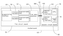
- FIG. 1 is a block diagram of a preferred embodiment of a motherboard of the present disclosure.
- FIG. 2 shows connection of a first data interface to a second data interface through connectors of the wiring of the motherboard of FIG. 1 .
- a preferred embodiment of a motherboard 100 includes a first circuit board 90 , a second circuit board 80 , and wiring 20 .
- the first circuit board 90 includes a programming interface 110 , a first data interface 120 , a plurality of programmable chips 60 and a plurality of jumpers 50 .
- the programming interface 110 such as a Joint Test Action Group (JTAG) interface, receives programming data.
- JTAG Joint Test Action Group
- the number of programmable chips 60 matches that of the jumpers 50 .
- Each programmable chips 60 is connected to the programming interface 110 through a jumper 50 .
- Each jumpers 50 such as a switch type jumper, selectively connects/disconnects the programmable chip 60 to/from the programming interface 110 .
- the first circuit board 90 can be disposed on a portable tray of a housing (not shown), such that the first circuit board 90 can be removed to allow the programmable chip 60 to be programmed without disassembling the housing.
- the first data interface 120 includes a plurality of data portions 220 isolated from each other. The number of data portions 220 matches that of the programmable chips 60 , and each programmable chips 60 corresponds to and is connected to a data portion 220 .
- the second circuit board 80 includes a CPU (central processing unit) 70 , a RAM (random access memory) unit 40 , and a plurality of second data interfaces 130 .
- the number of second data interface 130 matches that of the data portion 220 .
- the components (other than the programmable chip 60 ) on the second circuit board 80 and their arrangement match that of a frequently used motherboard and their details are omitted herefrom.
- One end of the wiring 20 has a first connector 300 disposed thereon, and the other end of the wiring 20 has a plurality of connectors 400 disposed thereon.
- the connector 300 includes a plurality of connection portions 310 , isolated from each other. The number of connection portions 310 matches that of the data portions 220 .
- each data portions 220 is correspondingly connected to one connection portion 310 .
- Each connector 400 corresponds to and is connected to one second data interface 130 .
- the first data interface 120 is connected to one end of the wiring 20 through the connector 300 .
- the second data interfaces 130 are connected to the other end of the wiring 20 through the connectors 400 .
- the first circuit board 90 is connected to the second circuit board 80 through the wiring 20 , and each programmable chip 60 can independently communicate with one second data interface 130 corresponding thereto.
- the portable tray with the first circuit board 90 mounted thereon is pulled out from the housing, disconnecting the first data interface 120 from the connector 300 .
- the programming interface 110 is connected to programming equipment.
- the jumper 50 corresponding to the programmable chip 60 to be programmed is closed when the other jumper 50 is opened.
- the programming interface 110 receives programming data, inputting to the programmable chip 60 through the jumper 50 which is closed.
- the motherboard 100 as disclosed concentrates the programmable chips 60 on the first circuit board 90 .
- the programmable chip 60 can be taken out from the housing and programmed without disassembling the housing, which is especially advantageous in programming multiple programmable chips 60 .
- the connector 300 includes a plurality of connection portions 310 , isolated from each other and thereby disconnecting the programmable chips 60 from the second circuit board 80 simply by unplugging the connector 300 .
Landscapes
- Engineering & Computer Science (AREA)
- Theoretical Computer Science (AREA)
- Computer Hardware Design (AREA)
- Power Engineering (AREA)
- Human Computer Interaction (AREA)
- Physics & Mathematics (AREA)
- General Engineering & Computer Science (AREA)
- General Physics & Mathematics (AREA)
- Design And Manufacture Of Integrated Circuits (AREA)
- Stored Programmes (AREA)
- Printing Elements For Providing Electric Connections Between Printed Circuits (AREA)
- Semiconductor Integrated Circuits (AREA)
Abstract
Description
Claims (4)
Applications Claiming Priority (2)
| Application Number | Priority Date | Filing Date | Title |
|---|---|---|---|
| CN201110041458.8 | 2011-02-17 | ||
| CN201110041458.8A CN102645955B (en) | 2011-02-17 | 2011-02-17 | Mainboard |
Publications (2)
| Publication Number | Publication Date |
|---|---|
| US20120212921A1 US20120212921A1 (en) | 2012-08-23 |
| US8553427B2 true US8553427B2 (en) | 2013-10-08 |
Family
ID=46652572
Family Applications (1)
| Application Number | Title | Priority Date | Filing Date |
|---|---|---|---|
| US13/072,831 Expired - Fee Related US8553427B2 (en) | 2011-02-17 | 2011-03-28 | Motherboard |
Country Status (3)
| Country | Link |
|---|---|
| US (1) | US8553427B2 (en) |
| CN (1) | CN102645955B (en) |
| TW (1) | TW201236527A (en) |
Cited By (2)
| Publication number | Priority date | Publication date | Assignee | Title |
|---|---|---|---|---|
| US20170199836A1 (en) * | 2014-05-30 | 2017-07-13 | Heba BEVAN | Manufacturing methods |
| US11825604B2 (en) | 2021-10-14 | 2023-11-21 | Unimicron Technology Corporation | Circuit board assembly |
Families Citing this family (4)
| Publication number | Priority date | Publication date | Assignee | Title |
|---|---|---|---|---|
| CN105988516B (en) * | 2015-02-12 | 2020-08-04 | 中兴通讯股份有限公司 | Processor daughter card, power panel adapting same and system board |
| CN106020911A (en) * | 2016-06-02 | 2016-10-12 | 广东盈科电子有限公司 | Microcontroller burning interface and circuit board connection multiplexing method |
| CN108848120B (en) * | 2018-05-02 | 2021-05-18 | 深圳创维-Rgb电子有限公司 | System for upgrading smart television mainboard software in batch and implementation method |
| CN114138694A (en) * | 2021-11-29 | 2022-03-04 | 杭州迪普科技股份有限公司 | Download interface module, chip burning method and device |
Citations (5)
| Publication number | Priority date | Publication date | Assignee | Title |
|---|---|---|---|---|
| US6496376B1 (en) * | 2000-06-02 | 2002-12-17 | John Plunkett | Modular backplane |
| US20040090761A1 (en) * | 2002-11-12 | 2004-05-13 | Compal Electronics, Inc. | Circuit board assembly with separable first and second circuit board devices |
| US20080106477A1 (en) * | 2004-06-29 | 2008-05-08 | Matsushita Electric Industrial Co., Ltd. | Collapsible Mobile Radio Device |
| US20080143609A1 (en) * | 2004-12-10 | 2008-06-19 | Matsushita Electric Industrial Co., Ltd. | Foldable Portable Radio Device |
| US20090175019A1 (en) * | 2007-03-20 | 2009-07-09 | Keiji Koyama | Circuit-board module and manufacturing method |
-
2011
- 2011-02-17 CN CN201110041458.8A patent/CN102645955B/en not_active Expired - Fee Related
- 2011-02-25 TW TW100106469A patent/TW201236527A/en unknown
- 2011-03-28 US US13/072,831 patent/US8553427B2/en not_active Expired - Fee Related
Patent Citations (5)
| Publication number | Priority date | Publication date | Assignee | Title |
|---|---|---|---|---|
| US6496376B1 (en) * | 2000-06-02 | 2002-12-17 | John Plunkett | Modular backplane |
| US20040090761A1 (en) * | 2002-11-12 | 2004-05-13 | Compal Electronics, Inc. | Circuit board assembly with separable first and second circuit board devices |
| US20080106477A1 (en) * | 2004-06-29 | 2008-05-08 | Matsushita Electric Industrial Co., Ltd. | Collapsible Mobile Radio Device |
| US20080143609A1 (en) * | 2004-12-10 | 2008-06-19 | Matsushita Electric Industrial Co., Ltd. | Foldable Portable Radio Device |
| US20090175019A1 (en) * | 2007-03-20 | 2009-07-09 | Keiji Koyama | Circuit-board module and manufacturing method |
Cited By (3)
| Publication number | Priority date | Publication date | Assignee | Title |
|---|---|---|---|---|
| US20170199836A1 (en) * | 2014-05-30 | 2017-07-13 | Heba BEVAN | Manufacturing methods |
| US10185694B2 (en) * | 2014-05-30 | 2019-01-22 | Heba BEVAN | Manufacturing methods for printed circuit boards |
| US11825604B2 (en) | 2021-10-14 | 2023-11-21 | Unimicron Technology Corporation | Circuit board assembly |
Also Published As
| Publication number | Publication date |
|---|---|
| TW201236527A (en) | 2012-09-01 |
| CN102645955B (en) | 2016-11-23 |
| CN102645955A (en) | 2012-08-22 |
| US20120212921A1 (en) | 2012-08-23 |
Similar Documents
| Publication | Publication Date | Title |
|---|---|---|
| US8553427B2 (en) | Motherboard | |
| US8959272B2 (en) | Interposer and intelligent multiplexer to provide a plurality of peripherial buses | |
| US20110197012A1 (en) | Computer motherboard | |
| US20060009048A1 (en) | Expansible interface for modularized printed circuit boards | |
| US7491066B1 (en) | Patch panel | |
| US10841246B2 (en) | Distributed core switching with orthogonal fabric card and line cards | |
| US20110007483A1 (en) | Electronic device and sata extension board thereof | |
| US9506980B2 (en) | Integrated circuit testing architecture | |
| US20120051716A1 (en) | Keyboard having video and audio recording function | |
| TWM519845U (en) | Composite connector (2) | |
| US10139871B2 (en) | Electronic device with circuit protection and assembling method thereof | |
| US10379139B2 (en) | Methods, systems and devices for testing circuit modules using a microbackplane interface | |
| US20150062832A1 (en) | U form-factor intelligent electronic device (ied) hardware platform with matching of ied wiring, from a non u form-factor ied hardware platform using adapter structure | |
| US9378074B2 (en) | Server system | |
| US8164919B2 (en) | Motherboard and relay device thereon | |
| US20170168111A1 (en) | Modular multiplexing interface assembly for reducing semiconductor testing index time | |
| US20120182682A1 (en) | Programming apparatus for system management bus interface memory chip | |
| CN103472267A (en) | LED signal switching device | |
| US20130238828A1 (en) | Expansion card with both PCI slot and PCIe slot | |
| US20120307438A1 (en) | Electronic device having multifunctional network interface port | |
| US9514076B2 (en) | Optimized two-socket/four-socket server architecture | |
| EP2682872B1 (en) | Interposer and intelligent multiplexer to provide a plurality of peripherial buses | |
| CN117940782A (en) | Test system and test device | |
| CN106774853A (en) | A kind of seismaesthesia feedback method and terminal | |
| CN203519651U (en) | LED signal switching device |
Legal Events
| Date | Code | Title | Description |
|---|---|---|---|
| AS | Assignment |
Owner name: HONG FU JIN PRECISION INDUSTRY (SHENZHEN) CO., LTD Free format text: ASSIGNMENT OF ASSIGNORS INTEREST;ASSIGNORS:LIU, MENG-ZHOU;WU, WEN-WU;REEL/FRAME:026028/0486 Effective date: 20110309 Owner name: HON HAI PRECISION INDUSTRY CO., LTD., TAIWAN Free format text: ASSIGNMENT OF ASSIGNORS INTEREST;ASSIGNORS:LIU, MENG-ZHOU;WU, WEN-WU;REEL/FRAME:026028/0486 Effective date: 20110309 |
|
| REMI | Maintenance fee reminder mailed | ||
| LAPS | Lapse for failure to pay maintenance fees |
Free format text: PATENT EXPIRED FOR FAILURE TO PAY MAINTENANCE FEES (ORIGINAL EVENT CODE: EXP.) |
|
| STCH | Information on status: patent discontinuation |
Free format text: PATENT EXPIRED DUE TO NONPAYMENT OF MAINTENANCE FEES UNDER 37 CFR 1.362 |
|
| FP | Lapsed due to failure to pay maintenance fee |
Effective date: 20171008 |