US8548017B1 - Amplitude combining method for phase locking fiber lasers - Google Patents

Amplitude combining method for phase locking fiber lasers Download PDF

Info

Publication number
US8548017B1
US8548017B1 US13/221,450 US201113221450A US8548017B1 US 8548017 B1 US8548017 B1 US 8548017B1 US 201113221450 A US201113221450 A US 201113221450A US 8548017 B1 US8548017 B1 US 8548017B1
Authority
US
United States
Prior art keywords
phase
output
adjusters
polarization
adjuster
Prior art date
Legal status (The legal status is an assumption and is not a legal conclusion. Google has not performed a legal analysis and makes no representation as to the accuracy of the status listed.)
Expired - Fee Related, expires
Application number
US13/221,450
Inventor
James P. O'Loughlin
Jeffry P. Heggemeier
Roy A. Hamil
Current Assignee (The listed assignees may be inaccurate. Google has not performed a legal analysis and makes no representation or warranty as to the accuracy of the list.)
US Air Force
Original Assignee
US Air Force
Priority date (The priority date is an assumption and is not a legal conclusion. Google has not performed a legal analysis and makes no representation as to the accuracy of the date listed.)
Filing date
Publication date
Application filed by US Air Force filed Critical US Air Force
Priority to US13/221,450 priority Critical patent/US8548017B1/en
Assigned to THE GOVERNMENT OF THE UNITED STATES AS REPRESENTED BY THE SECRETARY OF THE AIR FORCE reassignment THE GOVERNMENT OF THE UNITED STATES AS REPRESENTED BY THE SECRETARY OF THE AIR FORCE ASSIGNMENT OF ASSIGNORS INTEREST (SEE DOCUMENT FOR DETAILS). Assignors: HEGGEMEIER, JEFFRY P, HAMIL, ROY A, O'LOUGHLIN, JAMES P
Application granted granted Critical
Publication of US8548017B1 publication Critical patent/US8548017B1/en
Expired - Fee Related legal-status Critical Current
Adjusted expiration legal-status Critical

Links

Images

Classifications

    • HELECTRICITY
    • H01ELECTRIC ELEMENTS
    • H01SDEVICES USING THE PROCESS OF LIGHT AMPLIFICATION BY STIMULATED EMISSION OF RADIATION [LASER] TO AMPLIFY OR GENERATE LIGHT; DEVICES USING STIMULATED EMISSION OF ELECTROMAGNETIC RADIATION IN WAVE RANGES OTHER THAN OPTICAL
    • H01S3/00Lasers, i.e. devices using stimulated emission of electromagnetic radiation in the infrared, visible or ultraviolet wave range
    • H01S3/05Construction or shape of optical resonators; Accommodation of active medium therein; Shape of active medium
    • H01S3/06Construction or shape of active medium
    • H01S3/063Waveguide lasers, i.e. whereby the dimensions of the waveguide are of the order of the light wavelength
    • H01S3/067Fibre lasers
    • H01S3/06754Fibre amplifiers
    • HELECTRICITY
    • H01ELECTRIC ELEMENTS
    • H01SDEVICES USING THE PROCESS OF LIGHT AMPLIFICATION BY STIMULATED EMISSION OF RADIATION [LASER] TO AMPLIFY OR GENERATE LIGHT; DEVICES USING STIMULATED EMISSION OF ELECTROMAGNETIC RADIATION IN WAVE RANGES OTHER THAN OPTICAL
    • H01S3/00Lasers, i.e. devices using stimulated emission of electromagnetic radiation in the infrared, visible or ultraviolet wave range
    • H01S3/10Controlling the intensity, frequency, phase, polarisation or direction of the emitted radiation, e.g. switching, gating, modulating or demodulating
    • H01S3/13Stabilisation of laser output parameters, e.g. frequency or amplitude
    • H01S3/1307Stabilisation of the phase
    • HELECTRICITY
    • H01ELECTRIC ELEMENTS
    • H01SDEVICES USING THE PROCESS OF LIGHT AMPLIFICATION BY STIMULATED EMISSION OF RADIATION [LASER] TO AMPLIFY OR GENERATE LIGHT; DEVICES USING STIMULATED EMISSION OF ELECTROMAGNETIC RADIATION IN WAVE RANGES OTHER THAN OPTICAL
    • H01S3/00Lasers, i.e. devices using stimulated emission of electromagnetic radiation in the infrared, visible or ultraviolet wave range
    • H01S3/23Arrangements of two or more lasers not provided for in groups H01S3/02 - H01S3/22, e.g. tandem arrangements of separate active media
    • H01S3/2383Parallel arrangements

Definitions

  • the invention relates generally to a method for phase locking and coherently combining multiple laser amplifiers, and in particular to sweeping amplifier phase modulators in small steps over a 2 ⁇ range sequentially and selecting the phase of each that maximizes the combined output.
  • the intensity and, hence, the power available from a single-mode optical fiber is limited by either optical surface damage or nonlinear optical effects. These limitations can be overcome by coherent beam-combining of the output power from multiple optical fibers. Fine control of the optical phase is required for any multi-fiber approach.
  • FIG. 1 A simplified block diagram typical of this method is shown in FIG. 1 .
  • a master oscillator 1 is power divided 2 and provides the inputs to the N amplifiers 5 after first passing through modulators 3 and adjustable phase shifters 4 .
  • the method is based on tagging the N amplifiers 5 with a unique frequency.
  • the modulation process produces unique side-band frequencies on the signal related to the tag frequency.
  • the tag frequency sideband provides the means for identifying the signal of each specific amplifier output and in addition carries the phase information of the amplifier, which is necessary during the processing function of the method.
  • This modulation is accomplished by the Tag Oscillator 12 modulating the amplifier input via the modulator 3 .
  • the type of modulation may be phase modulation, frequency modulation or amplitude modulation, anyone of which can serve the purpose of the method.
  • the outputs of the amplifiers 5 are combined into a single output beam 10 by the coherent power combiner 6 .
  • a small sample of the output beam 10 is sampled by the coupler 7 which is input to the photodetector 8 .
  • the photodetector 8 output contains all of the individual amplifier outputs including the tagging sidebands.
  • This complex output is mixed individually 11 with each tag oscillator 12 .
  • the mixer 11 output is processed 13 to extract the phase of the corresponding amplifier 5 .
  • the processor 13 then generates an error signal that produces the drive signal for the phase shifter 4 based on a negative feedback process.
  • the negative feedback process is so configured as to correct the phase of each amplifier 5 output to match the phase of the other amplifiers and thereby provide the necessary condition to combine the power from each amplifier into a single coherent beam 10 .
  • One embodiment of the present invention employs an array of N laser amplifiers to achieve this objective.
  • This array of amplifiers is driven from a single master oscillator or source which is power divided to provide the same frequency input to each amplifier in the array.
  • Each such input is passed through a phase adjuster which is driven by a processor.
  • the combined output of the N amplifiers is sampled by a beam splitter and imaged onto a photodetector.
  • the photodetector output is proportional to the total combined power of all of the amplifiers and is the input to the processor.
  • the processor is designed to select one of the phase adjustors of a single amplifier.
  • the processor then scans the phase adjustor in small steps going from 0 to 2 ⁇ and fixes the phase shifter at the value that maximizes the detected total power output.
  • the processor selects the next phase adjustor and repeats the process of scanning the adjustor in small steps to again maximize the detected total power output for that phase adjuster and so on cycling through all the N phase adjusters.
  • the processor continuously repeats this scanning cycle and optimizing process and eventually reaches a state of phase adjustor settings that results in the maximum possible power output. This state corresponds to all of the amplifiers having the same phase, that is being phase locked, and thus producing the maximum possible combined power output.
  • the processor continuously operates such that any perturbations occurring from whatever source are corrected, thus maintain the optimum power combining performance.
  • the invention provides the simplest known means for obtaining the maximum possible combined total power output from an array of amplifiers to meet the objective of achieving a power level not otherwise possible.
  • a further embodiment maximizes the polarizations of the N amplifier signals in a similar manner and when combined with the phase adjuster process, maximizes the combined power output.
  • FIG. 1 is a simplified block diagram of a prior art frequency tagging method.
  • FIG. 2 is a diagram of the random amplitude method for combining laser amplifiers.
  • FIG. 3 is a simplified block diagram for combining M arrays of N amplifiers per array into a single array.
  • FIG. 4 is a block diagram for polarization optimization in addition to phase optimization to maximize the combined power output.
  • Amplitude combining for phase locking fiber lasers is a simple method for coherently combining optical fiber or other types of amplifiers. See FIG. 2 in which an array of N fiber amplifiers 17 , are driven by a common stable master oscillator 14 . A branch power divider 15 feeds each array amplifier 17 through an adjustable phase shifter 16 . The outputs of the array of N amplifiers are optically combined by a coherent power combiner 18 and a sample is split off 19 , spatially optically processed 23 , and sent to a photodetector 20 .
  • the optical processor 23 is a lens arrangement that focuses a far field spot on the photodetector 20 , such that the power in the central spot consists of contributions from every fiber amplifier element.
  • the output of the photodetector 20 is a signal proportional to the power in the combined array output 22 .
  • This signal is fed to a processor 21 and it is a measure of the level of the combined output power of the N amplifiers. These amplifiers initially have a random phase distribution; thus the power is less than the maximum possible level.
  • the processor functional operation is to select one of the N adjustable phase shifters 16 and sweep it over a 2 ⁇ range in small steps, while observing the total output power from the photodetector 20 . If a particular phase of the adjustable phase shifter is found that maximizes the total power then that phase shifter is set to that value and remains there unless and until it may undergo a change during a future sweep.
  • the number of steps is based on the power combining error as it relates to phase error. Typically 72 phase steps corresponding to 5 degree steps in 360 degrees would be quite acceptable for most applications. A 5 degree error corresponds to about a 0.08 percent power error (one minus the cosine of 5 degrees squared).
  • the processor 21 After completing a sweep of a first phase shifter, the processor 21 then selects the next adjustable phase shifter 16 from the array of N phase shifters and repeats the process, cycling through the remaining phase shifters until a cycle of stepping through the N phase shifters is completed. At this point each phase shifter is locked to the phase that maximized the combined output for its sweep. This cycle of stepping through the N phase shifters is then repeated over and over again during the laser operation. If any perturbation occurs for any reason during the laser operation, the continuous processor sweep operations will correct it to maintain the maximum possible power output. The absolute maximum possible power output will be achieved after a few sweep cycles by the processor.
  • the limitation of the maximum total number, N, of amplifiers that can be included is determined by the time it takes the processor to run through the required number of sequences, the resolution of the sweep step, and the rate and magnitude of the perturbations of the phase that occur.
  • the major advantage of the invention is the simplicity and performance compared to existing methods. The simplicity is quite evident by comparing FIG. 1 to FIG. 2 .
  • the invention closes the control loop directly for maximizing the combined total output power.
  • Other methods tend to function on control of the phase matching of the amplifiers by means of laboriously measuring the phase and processing that to maximize the output.
  • These phase measuring approaches are subject to perturbations of phase from thermally induced variations in optical path lengths that require addition methods and hardware to overcome.
  • some phase measuring based methods use tag modulation frequencies for each amplifier to sort out the individual phase of each amplifier for further processing. These tag frequencies remain in the output spectrum after combining.
  • the present invention does not pollute the spectrum with tag frequencies.
  • the invention inherently compensates for perturbations because they are internal to the processor control loop, thus no additional processing and hardware is necessary.
  • Another implementation is to use the invention to combine groups of sub-arrays, wherein each sub-array consists of N amplifiers and there are M groups of sub arrays. Each of the N amplifiers of each sub-array is power combined using the invention and then the group of M sub-arrays is itself power combined in-turn also using the invention; as shown in FIG. 3 .
  • the use of the invention to combine arrays of arrays provides for increased system power levels on the order of the number of amplifiers in a sub array, i.e., N 2 . It also logically follows the invention can be further extended to combine arrays of arrays of arrays, etc; thus in principle to power levels limited by other factors such as air breakdown, optics damage, etc.
  • Another implementation is to adapt the invention to include an additional set of components to optimize the polarization of the amplifier elements, as shown FIG. 4 . That is, in order to maximize the combined power of all of the amplifier elements it is necessary to maintain both the same phase and polarization.
  • the polarization optimization circuit operates in much the same manner as the phase optimization process.
  • the operation of the polarization optimization consists of the sequential processor first scanning and optimizing the power output using the phase scanning as previously explained. Then the processor 21 selects a polarization shifter 24 and scans over a polarization shift of 2 ⁇ while observing the combined power output signal from the photodetector 20 . If a polarization angle is detected that increases the power output; then that polarization angle is set and held until the next scan.
  • the processor 21 selects another polarization shifter and proceeds likewise through the remaining polarization shifters. Then the processor 21 selects a phase shifter and sequentially scans through all of the phase shifters; and continues the scan process alternating between polarization shifters and phase shifters ad infinitum. Thus both the phase and polarization are maintained at optimized settings to insure the maximum combined power output.

Abstract

A method for implementing a coherent laser beam combining system in which a master laser oscillator output is split into N signals, fed through N phase adjusters and N amplifiers and combined in a coherent power combiner. The output of the combiner is sampled and sent to a processor. The processor selects one of the N phase adjusters, sweeps the phase in small steps over a 2π range, and locks the phase of that adjuster to the phase that corresponds to the maximum value of the combiner sample for that sweep cycle. The process is repeated for all the remaining phase adjusters resulting in maximizing the combiner output. The sweep cycles are repeated continuously to correct any phase errors that may occur over time. A similar method can be used in which both the polarizations and the phases of the N signals are maximized to thereby maximize the output of the coherent power combiner.

Description

STATEMENT OF GOVERNMENT INTEREST
The conditions under which this invention was made are such as to entitle the Government of the United States under paragraph 1(a) of Executive Order 10096, as represented by the Secretary of the Air Force, to the entire right, title and interest therein, including foreign rights.
BACKGROUND OF THE INVENTION
The invention relates generally to a method for phase locking and coherently combining multiple laser amplifiers, and in particular to sweeping amplifier phase modulators in small steps over a 2π range sequentially and selecting the phase of each that maximizes the combined output.
The intensity and, hence, the power available from a single-mode optical fiber is limited by either optical surface damage or nonlinear optical effects. These limitations can be overcome by coherent beam-combining of the output power from multiple optical fibers. Fine control of the optical phase is required for any multi-fiber approach.
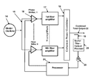
The most relevant prior art is embodied in the three patents of Thomas M. Shay, 7,058,098 B1, 7,187,492 B1, and 7,233,433 B1. These three patents have similar titles: “Self-referenced (or Self-synchronous) Locking of Optical Coherence by Single-Detector Electronic-Frequency Tagging”. They employ the same basic principle of frequency tagging, and phase detection and processing. A simplified block diagram typical of this method is shown in FIG. 1. A master oscillator 1 is power divided 2 and provides the inputs to the N amplifiers 5 after first passing through modulators 3 and adjustable phase shifters 4. The method is based on tagging the N amplifiers 5 with a unique frequency. The modulation process produces unique side-band frequencies on the signal related to the tag frequency. The tag frequency sideband provides the means for identifying the signal of each specific amplifier output and in addition carries the phase information of the amplifier, which is necessary during the processing function of the method. This modulation is accomplished by the Tag Oscillator 12 modulating the amplifier input via the modulator 3. The type of modulation may be phase modulation, frequency modulation or amplitude modulation, anyone of which can serve the purpose of the method.
These three patents relate to the different types or combinations of types of modulation; however, the basic overall method is the same. The outputs of the amplifiers 5 are combined into a single output beam 10 by the coherent power combiner 6. A small sample of the output beam 10 is sampled by the coupler 7 which is input to the photodetector 8. The photodetector 8 output contains all of the individual amplifier outputs including the tagging sidebands. This complex output is mixed individually 11 with each tag oscillator 12. The mixer 11 output is processed 13 to extract the phase of the corresponding amplifier 5. The processor 13 then generates an error signal that produces the drive signal for the phase shifter 4 based on a negative feedback process. The negative feedback process is so configured as to correct the phase of each amplifier 5 output to match the phase of the other amplifiers and thereby provide the necessary condition to combine the power from each amplifier into a single coherent beam 10.
SUMMARY
In applications requiring a higher laser power than that of a single source, it is necessary to coherently combine a plurality of the lower power sources to accomplish the high power requirement. To accomplish this all of the lesser power sources must be at the same frequency and phase so that they will combine to provide a total coherent high power combined output.
One embodiment of the present invention employs an array of N laser amplifiers to achieve this objective. This array of amplifiers is driven from a single master oscillator or source which is power divided to provide the same frequency input to each amplifier in the array. Each such input is passed through a phase adjuster which is driven by a processor. The combined output of the N amplifiers is sampled by a beam splitter and imaged onto a photodetector. The photodetector output is proportional to the total combined power of all of the amplifiers and is the input to the processor.
The processor is designed to select one of the phase adjustors of a single amplifier. The processor then scans the phase adjustor in small steps going from 0 to 2π and fixes the phase shifter at the value that maximizes the detected total power output. The processor then selects the next phase adjustor and repeats the process of scanning the adjustor in small steps to again maximize the detected total power output for that phase adjuster and so on cycling through all the N phase adjusters. The processor continuously repeats this scanning cycle and optimizing process and eventually reaches a state of phase adjustor settings that results in the maximum possible power output. This state corresponds to all of the amplifiers having the same phase, that is being phase locked, and thus producing the maximum possible combined power output. In addition the processor continuously operates such that any perturbations occurring from whatever source are corrected, thus maintain the optimum power combining performance. The invention provides the simplest known means for obtaining the maximum possible combined total power output from an array of amplifiers to meet the objective of achieving a power level not otherwise possible.
A further embodiment maximizes the polarizations of the N amplifier signals in a similar manner and when combined with the phase adjuster process, maximizes the combined power output.
BRIEF DESCRIPTION OF THE DRAWINGS
FIG. 1 is a simplified block diagram of a prior art frequency tagging method.
FIG. 2 is a diagram of the random amplitude method for combining laser amplifiers.
FIG. 3 is a simplified block diagram for combining M arrays of N amplifiers per array into a single array.
FIG. 4 is a block diagram for polarization optimization in addition to phase optimization to maximize the combined power output.
DESCRIPTION OF THE PREFERRED EMBODIMENT
Amplitude combining for phase locking fiber lasers is a simple method for coherently combining optical fiber or other types of amplifiers. See FIG. 2 in which an array of N fiber amplifiers 17, are driven by a common stable master oscillator 14. A branch power divider 15 feeds each array amplifier 17 through an adjustable phase shifter 16. The outputs of the array of N amplifiers are optically combined by a coherent power combiner 18 and a sample is split off 19, spatially optically processed 23, and sent to a photodetector 20. The optical processor 23 is a lens arrangement that focuses a far field spot on the photodetector 20, such that the power in the central spot consists of contributions from every fiber amplifier element. The output of the photodetector 20 is a signal proportional to the power in the combined array output 22. This signal is fed to a processor 21 and it is a measure of the level of the combined output power of the N amplifiers. These amplifiers initially have a random phase distribution; thus the power is less than the maximum possible level. The processor functional operation is to select one of the N adjustable phase shifters 16 and sweep it over a 2π range in small steps, while observing the total output power from the photodetector 20. If a particular phase of the adjustable phase shifter is found that maximizes the total power then that phase shifter is set to that value and remains there unless and until it may undergo a change during a future sweep. The number of steps is based on the power combining error as it relates to phase error. Typically 72 phase steps corresponding to 5 degree steps in 360 degrees would be quite acceptable for most applications. A 5 degree error corresponds to about a 0.08 percent power error (one minus the cosine of 5 degrees squared).
After completing a sweep of a first phase shifter, the processor 21 then selects the next adjustable phase shifter 16 from the array of N phase shifters and repeats the process, cycling through the remaining phase shifters until a cycle of stepping through the N phase shifters is completed. At this point each phase shifter is locked to the phase that maximized the combined output for its sweep. This cycle of stepping through the N phase shifters is then repeated over and over again during the laser operation. If any perturbation occurs for any reason during the laser operation, the continuous processor sweep operations will correct it to maintain the maximum possible power output. The absolute maximum possible power output will be achieved after a few sweep cycles by the processor.
The limitation of the maximum total number, N, of amplifiers that can be included is determined by the time it takes the processor to run through the required number of sequences, the resolution of the sweep step, and the rate and magnitude of the perturbations of the phase that occur.
The major advantage of the invention is the simplicity and performance compared to existing methods. The simplicity is quite evident by comparing FIG. 1 to FIG. 2. Instead of identifying and processing a plethora of phases, the invention closes the control loop directly for maximizing the combined total output power. Other methods tend to function on control of the phase matching of the amplifiers by means of laboriously measuring the phase and processing that to maximize the output. These phase measuring approaches are subject to perturbations of phase from thermally induced variations in optical path lengths that require addition methods and hardware to overcome. In addition some phase measuring based methods use tag modulation frequencies for each amplifier to sort out the individual phase of each amplifier for further processing. These tag frequencies remain in the output spectrum after combining. The present invention does not pollute the spectrum with tag frequencies. In addition the invention inherently compensates for perturbations because they are internal to the processor control loop, thus no additional processing and hardware is necessary.
Another implementation is to use the invention to combine groups of sub-arrays, wherein each sub-array consists of N amplifiers and there are M groups of sub arrays. Each of the N amplifiers of each sub-array is power combined using the invention and then the group of M sub-arrays is itself power combined in-turn also using the invention; as shown in FIG. 3. The use of the invention to combine arrays of arrays provides for increased system power levels on the order of the number of amplifiers in a sub array, i.e., N2. It also logically follows the invention can be further extended to combine arrays of arrays of arrays, etc; thus in principle to power levels limited by other factors such as air breakdown, optics damage, etc.
Another implementation is to adapt the invention to include an additional set of components to optimize the polarization of the amplifier elements, as shown FIG. 4. That is, in order to maximize the combined power of all of the amplifier elements it is necessary to maintain both the same phase and polarization. The polarization optimization circuit operates in much the same manner as the phase optimization process. The operation of the polarization optimization consists of the sequential processor first scanning and optimizing the power output using the phase scanning as previously explained. Then the processor 21 selects a polarization shifter 24 and scans over a polarization shift of 2π while observing the combined power output signal from the photodetector 20. If a polarization angle is detected that increases the power output; then that polarization angle is set and held until the next scan. The processor 21 then selects another polarization shifter and proceeds likewise through the remaining polarization shifters. Then the processor 21 selects a phase shifter and sequentially scans through all of the phase shifters; and continues the scan process alternating between polarization shifters and phase shifters ad infinitum. Thus both the phase and polarization are maintained at optimized settings to insure the maximum combined power output.

Claims (5)

The invention claimed is:
1. A method for implementing a coherent laser beam combining system in which phases of N fiber amplifier outputs are maximized, the method comprising:
a. splitting the output of a master oscillator laser into an array of N signals;
b. feeding said N signals into N optical phase adjusters;
c. optically amplifying the output of said N phase adjusters with N fiber amplifiers;
d. combining said N amplified signals in a coherent power combiner to produce a combined total output signal;
e. sampling said combined total output signal and processing said sampled output through a far field spatial imaging optics system and thence to a photodetector, wherein the photodetector output is a voltage which is proportional to a combined far field power;
f. selecting one of the N phase adjusters using a processor and then sweeping the phase of said adjuster in small steps over a 2π range and locking said phase adjuster to the phase that corresponds to a maximum photodetector output voltage as the phase is stepped through the 2π range;
g. sequentially selecting the next phase adjuster of the N phase adjusters and repeating step f for that phase adjuster and so on for the remaining phase adjusters until the entire array of N phase adjusters are locked into phases that maximize said photodetector output voltage, thereby maximizing the output of said coherent power combiner; and
h. continually repeating steps f and g to thereby correct any phase errors that may occur over time.
2. The method for implementing a coherent laser beam combining system of claim 1, wherein said sweep of each phase adjuster in small steps over a 2π range consists of approximately 72 phase steps.
3. The method for implementing a coherent laser beam combining system in which a group of M sub-arrays are combined, each sub-array comprised of N laser amplifiers, the method comprising a cycle of maximizing the output of each sub-array using the method of claim 1 followed by maximizing the thus maximized output of said group of M sub-arrays by the method of claim 1 and continually repeating this cycle to thereby correct any phase errors that may occur over time.
4. A method for implementing a coherent laser beam combining system in which both phases and polarizations of N fiber amplifier outputs are maximized, the method comprising:
a. splitting the output of a master oscillator laser into an array of N signals;
b. feeding said N signals into N polarization adjusters and then into N optical phase adjusters;
c. optically amplifying the output of said N polarization adjusters and N phase adjusters with N fiber amplifiers;
d. combining said N amplified signals in a coherent power combiner to produce a combined total output signal;
e. sampling said combined total output signal and processing said sampled output through a far field spatial imaging optics system and thence to a photodetector, wherein the photodetector output is a voltage which is proportional to a combined far field power;
f. selecting one of the N phase adjusters using a processor and then sweeping the phase of said adjuster in small steps over a 2π range and locking said phase adjuster to the phase that corresponds to a maximum photodetector output voltage as the phase is stepped through the 2π range;
g. sequentially selecting the next phase adjuster of the N phase adjusters and repeating step f for that phase adjuster and so on for the remaining phase adjusters until the entire array of N phase adjusters are locked into phases that maximize said photodetector output voltage, thereby maximizing the output of said coherent power combiner;
i. selecting one of the N polarization adjusters using a processor and then sweeping the polarization of said adjuster over a 2π range and locking said polarization adjuster to the polarization that corresponds to the maximum photodetector output voltage as the polarization is swept through the 2π range;
j. sequentially selecting the next polarization adjuster of the N polarization adjusters and repeating step i for that polarization adjuster and so on for the remaining polarization adjusters until the entire array of N polarization adjusters are locked into polarizations that maximize said photodetector output voltage, thereby maximizing the output of said coherent power combiner;
k. continually repeating steps f through i to thereby correct any polarization or phase errors that may occur over time.
5. The method for implementing a coherent laser beam combining system in which both the phase and the polarization of N fiber amplifiers are maximized of claim 4, wherein said sweep of each phase adjuster in small steps over a 2π range consists of approximately 72 phase steps.
US13/221,450 2011-08-30 2011-08-30 Amplitude combining method for phase locking fiber lasers Expired - Fee Related US8548017B1 (en)

Priority Applications (1)

Application Number Priority Date Filing Date Title
US13/221,450 US8548017B1 (en) 2011-08-30 2011-08-30 Amplitude combining method for phase locking fiber lasers

Applications Claiming Priority (1)

Application Number Priority Date Filing Date Title
US13/221,450 US8548017B1 (en) 2011-08-30 2011-08-30 Amplitude combining method for phase locking fiber lasers

Publications (1)

Publication Number Publication Date
US8548017B1 true US8548017B1 (en) 2013-10-01

Family

ID=49229907

Family Applications (1)

Application Number Title Priority Date Filing Date
US13/221,450 Expired - Fee Related US8548017B1 (en) 2011-08-30 2011-08-30 Amplitude combining method for phase locking fiber lasers

Country Status (1)

Country Link
US (1) US8548017B1 (en)

Cited By (5)

* Cited by examiner, † Cited by third party
Publication number Priority date Publication date Assignee Title
US20130315271A1 (en) * 2012-05-24 2013-11-28 Gregory D. Goodno Coherent laser array control system and method
WO2017004013A1 (en) * 2015-07-01 2017-01-05 Northrop Grumman Systems Corporation Multichannel controller
JP2020005000A (en) * 2019-09-27 2020-01-09 株式会社フジクラ Photodetector and laser device
US20210175680A1 (en) * 2017-11-07 2021-06-10 Civan Advanced Technologies Ltd. Optical phased array dynamic beam shaping with noise correction
US11940321B2 (en) 2018-06-22 2024-03-26 Fujikura Ltd. Photodetection device and laser device

Citations (2)

* Cited by examiner, † Cited by third party
Publication number Priority date Publication date Assignee Title
US7058098B1 (en) * 2005-11-29 2006-06-06 The United States Of America As Represented By The Secretary Of The Air Force Self-synchronous locking of optical coherence by single-detector electronic-frequency tagging
US7187492B1 (en) * 2005-08-30 2007-03-06 The United States Of America As Represented By The Secretary Of The Air Force Self-referenced locking of optical coherence by single-detector electronic-frequency tagging

Patent Citations (3)

* Cited by examiner, † Cited by third party
Publication number Priority date Publication date Assignee Title
US7187492B1 (en) * 2005-08-30 2007-03-06 The United States Of America As Represented By The Secretary Of The Air Force Self-referenced locking of optical coherence by single-detector electronic-frequency tagging
US7233433B1 (en) * 2005-08-30 2007-06-19 United States Of America As Represented By The Secretary Of The Air Force Self-reference locking of optical coherence by single-detector electronic-frequency tagging
US7058098B1 (en) * 2005-11-29 2006-06-06 The United States Of America As Represented By The Secretary Of The Air Force Self-synchronous locking of optical coherence by single-detector electronic-frequency tagging

Cited By (8)

* Cited by examiner, † Cited by third party
Publication number Priority date Publication date Assignee Title
US20130315271A1 (en) * 2012-05-24 2013-11-28 Gregory D. Goodno Coherent laser array control system and method
US8792526B2 (en) * 2012-05-24 2014-07-29 Northrop Grumman Systems Corporation Coherent laser array control system and method
WO2017004013A1 (en) * 2015-07-01 2017-01-05 Northrop Grumman Systems Corporation Multichannel controller
JP2018521373A (en) * 2015-07-01 2018-08-02 ノースロップ グルマン システムズ コーポレーションNorthrop Grumman Systems Corporation Multi-channel controller
US20210175680A1 (en) * 2017-11-07 2021-06-10 Civan Advanced Technologies Ltd. Optical phased array dynamic beam shaping with noise correction
US11646543B2 (en) * 2017-11-07 2023-05-09 Civan Advanced Technologies Ltd. Optical phased array dynamic beam shaping with noise correction
US11940321B2 (en) 2018-06-22 2024-03-26 Fujikura Ltd. Photodetection device and laser device
JP2020005000A (en) * 2019-09-27 2020-01-09 株式会社フジクラ Photodetector and laser device

Similar Documents

Publication Publication Date Title
US8548017B1 (en) Amplitude combining method for phase locking fiber lasers
US7884997B2 (en) System and method for coherent beam combination
CN103674926B (en) Optical devices
CN102305591B (en) Multi-frequency synchronization phase laser ranging device and method based on dual-acousto-optic shift frequency
CN102176021B (en) Ranging device based on laser phase method
CN1639550B (en) Method and apparatus for optical beam alignment detection and control
CN103986053A (en) Frequency lock system and method of continuous tunable laser
CN111638202B (en) Double-optical-comb coherent anti-Stokes Raman spectrum detection system for localized rapid time-delay scanning
CN101408623A (en) Up-conversion imaging system of broad band synthetic aperture
CN101907513B (en) Diffraction property low-light test system and method of acousto-optic tunable filter (AOTF)
CN103576162A (en) Laser radar device and method for measuring target object distance through device
CN111948626A (en) Optical fiber phased array multi-beam scanning system based on array detector
WO2021227265A1 (en) Device and method for measuring absolute distance by variable synthetic wavelength locked to dynamic sideband
CN102692394A (en) Two-dimensional imaging method and device based on thermal lens effect
CN107870441B (en) Optical fiber laser coherent synthesis method based on digital holography
US9812840B2 (en) System for phasing a large number of laser sources
CN113281278A (en) Rapid ultrahigh-resolution transient absorption spectrum measuring device and measuring method
CN111665222A (en) Femtosecond pumping detection system and method
US9588055B2 (en) Defect inspection apparatus and defect inspection method
CN214893682U (en) Quick ultrahigh-resolution transient absorption spectrum measuring device
US8922771B2 (en) Multichannel polarization stabilizer
CN111912608B (en) Test method and device for vibration sensitivity of transportable optical reference cavity
CN201749021U (en) Dim light test device of diffraction performance of acousto-optic turnable filter
CN110186568B (en) Photon mixing terahertz wave detection device
US11486792B2 (en) Tunable light source for optical fiber proximity and testing

Legal Events

Date Code Title Description
AS Assignment

Owner name: THE GOVERNMENT OF THE UNITED STATES AS REPRESENTED

Free format text: ASSIGNMENT OF ASSIGNORS INTEREST;ASSIGNORS:O'LOUGHLIN, JAMES P;HEGGEMEIER, JEFFRY P;HAMIL, ROY A;SIGNING DATES FROM 20110823 TO 20110830;REEL/FRAME:026830/0412

STCF Information on status: patent grant

Free format text: PATENTED CASE

FPAY Fee payment

Year of fee payment: 4

FEPP Fee payment procedure

Free format text: MAINTENANCE FEE REMINDER MAILED (ORIGINAL EVENT CODE: REM.); ENTITY STATUS OF PATENT OWNER: LARGE ENTITY

LAPS Lapse for failure to pay maintenance fees

Free format text: PATENT EXPIRED FOR FAILURE TO PAY MAINTENANCE FEES (ORIGINAL EVENT CODE: EXP.); ENTITY STATUS OF PATENT OWNER: LARGE ENTITY

STCH Information on status: patent discontinuation

Free format text: PATENT EXPIRED DUE TO NONPAYMENT OF MAINTENANCE FEES UNDER 37 CFR 1.362

FP Lapsed due to failure to pay maintenance fee

Effective date: 20211001