US8514636B2 - Semiconductor storage device - Google Patents
Semiconductor storage device Download PDFInfo
- Publication number
- US8514636B2 US8514636B2 US13/235,391 US201113235391A US8514636B2 US 8514636 B2 US8514636 B2 US 8514636B2 US 201113235391 A US201113235391 A US 201113235391A US 8514636 B2 US8514636 B2 US 8514636B2
- Authority
- US
- United States
- Prior art keywords
- node
- transistor
- data
- level
- bit line
- Prior art date
- Legal status (The legal status is an assumption and is not a legal conclusion. Google has not performed a legal analysis and makes no representation as to the accuracy of the status listed.)
- Active, expires
Links
Images


Classifications
-
- G—PHYSICS
- G11—INFORMATION STORAGE
- G11C—STATIC STORES
- G11C11/00—Digital stores characterised by the use of particular electric or magnetic storage elements; Storage elements therefor
- G11C11/56—Digital stores characterised by the use of particular electric or magnetic storage elements; Storage elements therefor using storage elements with more than two stable states represented by steps, e.g. of voltage, current, phase, frequency
- G11C11/5621—Digital stores characterised by the use of particular electric or magnetic storage elements; Storage elements therefor using storage elements with more than two stable states represented by steps, e.g. of voltage, current, phase, frequency using charge storage in a floating gate
- G11C11/5642—Sensing or reading circuits; Data output circuits
-
- G—PHYSICS
- G11—INFORMATION STORAGE
- G11C—STATIC STORES
- G11C16/00—Erasable programmable read-only memories
- G11C16/02—Erasable programmable read-only memories electrically programmable
- G11C16/06—Auxiliary circuits, e.g. for writing into memory
- G11C16/10—Programming or data input circuits
-
- G—PHYSICS
- G11—INFORMATION STORAGE
- G11C—STATIC STORES
- G11C16/00—Erasable programmable read-only memories
- G11C16/02—Erasable programmable read-only memories electrically programmable
- G11C16/06—Auxiliary circuits, e.g. for writing into memory
- G11C16/26—Sensing or reading circuits; Data output circuits
Definitions
- Embodiments described herein relate generally to a semiconductor storage device, which communicates data with a memory cell, which holds the data, while enabling to reduce a peak current and error in data reading.
- a memory capable of holding multi-level data in the memory cell has been developed.
- a function of a sense amplifier is also required to support multi-level. That is, in the memory, there is a single-level cell (SLC) capable of storing 1-bit data in the memory cell, a multi-level cell (MLC) capable of storing multi-bit data in the memory cell and the like.
- SLC single-level cell
- MLC multi-level cell
- FIG. 1 is a configuration example of a NAND flash memory according to a first embodiment
- FIG. 2 is a threshold distribution of memory cells according to the first embodiment
- FIG. 3 is a block diagram of a voltage generating circuit according to the first embodiment
- FIG. 4 is a configuration example of a sense amplifier according to the first embodiment
- FIG. 5 is a block diagram of a sense unit according to the first embodiment
- FIGS. 6-9 are a schematic diagram illustrating a read operation of the sense unit according to the first embodiment
- FIGS. 10-13 are a schematic diagram illustrating a write operation of the sense unit according to the first embodiment
- FIGS. 14-17 are a schematic diagram illustrating the write-verify operation of the sense unit according to the first embodiment
- FIG. 18 is a schematic diagram illustrating a collective detecting operation of the sense unit according to the first embodiment
- FIG. 19 is a schematic diagram illustrating a rewrite operation of the sense unit according to the first embodiment
- FIG. 20 is a schematic diagram illustrating an erase operation according to the first embodiment
- FIGS. 21-23 are a schematic diagram of the sense unit illustrating an erase-verify operation of an even-numbered bit line BL according to the first embodiment
- FIGS. 24-26 are a schematic diagram of the sense unit illustrating the erase-verify operation of an odd-numbered bit line BL according to the first embodiment
- FIGS. 27-29 are a schematic diagram illustrating an arithmetic operation of the sense unit according to the first embodiment
- FIG. 30 is a schematic diagram of a sense unit according to a first variation of the first embodiment
- FIG. 31 is a schematic diagram of a sense unit according to a second variation of the first embodiment.
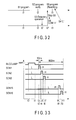
- FIG. 32 is a schematic diagram illustrating a detecting operation of the sense unit according to the second variation of the first embodiment
- FIG. 33 is a time chart of a signal SEN according to a second embodiment
- FIG. 34 is a schematic diagram of a sense unit according to a third embodiment.
- FIGS. 35-37 are a schematic diagram illustrating an erase-verify operation of the sense unit according to the third embodiment.
- FIG. 38 is a schematic diagram of a sense unit according to a fourth embodiment.
- FIG. 39 is a schematic diagram of a sense unit according to a variation of the fourth embodiment.
- FIG. 40 is a block diagram illustrating an entire configuration example of a semiconductor storage device according to the fifth embodiment.
- FIGS. 41 and 42 are a view illustrating a data read operation of the sense unit according to the first embodiment
- FIG. 43 is a view illustrating a write-verify operation of the sense unit according to the first embodiment
- FIGS. 44-46 are a view illustrating a data erase/erase-verify operation of the sense unit according to the fifth embodiment
- FIGS. 47-52 are a view illustrating a data erase/erase-verify operation of the sense unit according to the fifth embodiment
- FIG. 53 is a view illustrating a NOT arithmetic operation of the sense unit according to the fifth embodiment.
- FIGS. 54-56 are a view illustrating a data erase/erase-verify operation of the sense unit according to the fifth embodiment
- FIGS. 57-61 are a view illustrating a cell current monitoring operation of the sense unit according to the fifth embodiment.
- FIG. 62 is an equivalent circuit diagram illustrating the sense unit according to the sixth embodiment.
- FIGS. 63-68 are a view illustrating a data read operation of the sense unit according to the sixth embodiment.
- FIGS. 69-72 are a view illustrating a data write operation of the sense unit according to the sixth embodiment.
- FIGS. 73-86 are a view illustrating a data erase/erase-verify operation of the sense unit according to the fifth embodiment
- FIGS. 87-91 are a view illustrating a NOT arithmetic operation of the sense unit according to the sixth embodiment.
- FIGS. 92 , 93 are a view illustrating an operation to transfer data of the sense unit according to the six embodiment
- FIGS. 94 , 95 are a schematic diagram illustrating the switching current flows through the sense unit according to the sixth embodiment.
- FIG. 96 is a distribution of a cell current, which flows to the memory cell transistor MT according to the seventh embodiment
- FIG. 97 is a circuit example of the sense unit according to the seventh embodiment.
- FIGS. 98 , 99 are a schematic diagram illustrating the read operation according to the seventh embodiment.
- FIG. 100 is a time chart illustrating the read operation according to the seventh embodiment.
- FIG. 101A is a time chart obtained by enlarging FIG. 100 in which attention is focused on a Read Margin
- FIG. 101B is a time chart according to a comparative example of the seventh embodiment in which attention is focused on the Read Margin;
- FIG. 102A is a time chart illustrating a read operation of the semiconductor storage device according to the seventh embodiment and FIG. 102B is I-V characteristics of the semiconductor storage device according to the seventh embodiment;
- FIG. 103 is a schematic diagram illustrating an operation of boost down of a sense unit according to the eighth embodiment.
- FIG. 104 is a schematic diagram illustrating the operation of the boost down of a sense unit according to the ninth embodiment.
- a semiconductor storage device includes a memory cell array, an even-numbered bit line, an odd-numbered bit line, and a plurality of sense amplifiers.
- the memory cell array includes a plurality of memory cells.
- the even-numbered bit line connects to the memory cells connected to an even-numbered column.
- the odd-numbered bit line connects to the memory cells connected to an odd-numbered column adjacent to the even-numbered column.
- Each of the plurality of sense amplifiers selectively connect to the odd-numbered bit line and the even-numbered bit line.
- the each of the sense amplifiers includes a latch circuit, a first transistor, a second transistor, and a third transistor.
- the latch circuit includes a first node and a second node, which holds the data supplied to the first node.
- a gate of the first transistor connects to wiring selectively connected to the even-numbered bit line or the odd-numbered bit line.
- One end of a current pathway of the first transistor connects to the first node of the latch circuit.
- the first transistor supplies read data to the latch circuit on the basis of a potential of the wiring when reading the data.
- the second transistor is connected between the first node of the latch circuit and the wiring.
- the second transistor transfers the data held by the latch circuit to the wiring when performing arithmetic of the data.
- the third transistor is connected between the second node of the latch circuit and the wiring. The third transistor transfers the data held by the latch circuit to the wiring when writing the data.
- An area of a semiconductor storage device is reduced by omitting a transistor, which is not required in operation, of a sense amplifier capable of reading and writing data from and to a memory cell transistor MT, which holds 2-level data.
- the semiconductor storage device is provided with a memory cell array 1 , a row decoder 2 , a driver circuit 3 , a voltage generating circuit 4 , a bit line clamp driver 5 (hereinafter, a BLC driver 5 ), an re-channel MOS transistor group 6 , a data input/output circuit 7 , a controller 8 , a source line SL driver 9 , a well driver 10 , and a sense amplifier 11 .
- a BLC driver 5 bit line clamp driver 5
- the memory cell array 1 is provided with blocks BLK 0 to BLKs (s is a natural number), each of which includes a plurality of nonvolatile memory cell transistors MT.
- Each of the blocks BLK 0 to BLKs is provided with a plurality of NAND strings 15 obtained by connecting the nonvolatile memory cell transistors MT in series.
- Each of the NAND strings 15 includes 64 memory cell transistors MT, for example, and selection transistors ST 1 and ST 2 .
- the memory cell transistor MT is capable of holding 2-or-higher-level data.
- a structure of the memory cell transistor MT is a MONOS structure including a charge accumulation layer (for example, an insulating film) formed on a semiconductor substrate with a gate insulating film interposed therebetween, an insulating film (hereinafter, referred to as a block layer) with a dielectric constant higher than that of the charge accumulation layer formed on the charge accumulation layer, and further, a control gate formed on the block layer.
- the structure of the memory cell transistor MT may also be of an FG type.
- the FG type structure is one that includes a floating gate (conductive layer) formed on a p-type semiconductor substrate with the gate insulating film interposed therebetween and the control gate formed on the floating gate with an intergate insulating film interposed therebetween.
- the control gate of the memory cell transistor MT is electrically connected to a word line, a drain thereof is electrically connected to a bit line, and a source thereof is electrically connected to a source line.
- the memory cell transistor MT is an re-channel MOS transistor.
- the number of the memory cell transistors MT is not limited to 64, and may be 128, 256, 512 and the like, and there is no limitation.
- adjacent memory cell transistors MT share the source and the drain.
- the memory cell transistors MT are arranged between the selection transistors ST 1 and ST 2 such that current pathways thereof are connected in series.
- a drain region on one end side of the memory cell transistors MT connected in series is connected to a source region of the selection transistor ST 1 and a source region on the other end side thereof is connected to a drain region of the selection transistor ST 2 .
- control gates of the memory cell transistors MT on the same row are connected in common to any of word lines WL 0 to WL 63 and gate electrodes of the selection transistors ST 1 and ST 2 of the memory cell transistors MT on the same row are connected in common to select gate lines SGD 1 and SGS 1 , respectively.
- word lines WL 0 to WL 63 are not distinguished from one another, they are sometimes simply referred to as word lines WL.
- drains of the selection transistors ST 1 on the same column are connected in common to any of bit lines BL 0 to BLn.
- bit lines BL 0 to BLn are not distinguished from one another, they also are collectively referred to as bit lines BL (n is a natural number).
- Sources of the selection transistors ST 2 are connected in common to a source line SL.
- the data is collectively written to a plurality of memory cell transistors MT connected to the same word line WL and this unit is referred to as a page. Further, the data is collectively erased from a plurality of memory cell transistors MT in a block BLK unit.
- FIG. 2 is a graph in which the threshold distribution is represented along an abscissa axis and the number of the memory cell transistors MT is represented along a ordinate axis.
- each of the memory cell transistors MT may hold the 2-level data (1-bit data), for example. That is to say, the memory cell transistor MT may hold two types of data, which are ‘1’ and ‘0’ in ascending order of a threshold voltage Vth.
- a threshold voltage Vth 0 of the data ‘1’ in the memory cell transistor MT satisfies Vth 0 ⁇ V 01 .
- a threshold voltage Vth 1 of the data ‘0’ satisfies V 01 ⁇ Vth 1 .
- the memory cell transistor MT may hold the 1-bit data, which are the data ‘0’ or the data ‘1’, according to a threshold.
- the memory cell transistor MT is set to the data ‘1’ (for example, a negative voltage) in an erased state and is set to a positive threshold voltage by writing the data and injecting charge to the charge accumulation layer.
- the row decoder 2 is described.
- the row decoder 2 is provided with a block decoder 20 and n-channel MOS transistors 21 to 23 .
- the block decoder 20 decodes a block address given by the controller 8 at the time of a write operation, read operation, and erasing of the data and selects the block BLK based on a result. That is to say, the block decoder 20 selects a control line TG to which the MOS transistors 21 to 23 corresponding to the block BLK including a selected memory cell transistor MT is connected to turn on the MOS transistors 21 to 23 . At that time, a block selection signal is output from the block decoder 20 .
- the block selection signal is the signal with which the row decoder 2 selects any of a plurality of memory blocks BLK 0 to BLKs when reading, writing, and erasing the data. Also, according to this, the row decoder 2 selects a row direction of the memory cell array 1 corresponding to a selected block BLK. That is to say, based on the selection signal given by the block decoder 20 , the row decoder 2 applies a voltage given by the driver circuit 3 to the select gate lines SGD 1 and SGS 1 and the word lines WL 0 to WL 63 .
- the driver circuit 3 is provided with select gate line drivers 31 and 32 provided for the select gate lines SGD 1 and SGS 1 , respectively, and a word line driver 33 provided for each of the word lines WL.
- select gate line drivers 31 and 32 provided for the select gate lines SGD 1 and SGS 1 , respectively, and a word line driver 33 provided for each of the word lines WL.
- the word line drivers 33 and the select gate line drivers 31 and 32 are connected in common to the 64 word lines WL, for example, and the select gate lines SGD 1 and SGS 1 provided for each of the blocks BLK 0 to BLKs.
- the block BLK is selected according to a decode result of a page address given by the controller 8 .
- the word line driver 33 transfers a voltage to the control gate of the memory cell transistor MT provided in a selected block BLK through a selected word line WL.
- the select gate line driver 31 transfers the required voltage to a gate of the selection transistor ST 1 through the select gate line SGD 1 corresponding to the selected block BLK.
- the select gate line driver 31 transfers a signal sgd to the gate of the selection transistor ST 1 .
- the select gate line driver 31 transfers the signal sgd to the gate of the selection transistor ST 1 , for example, through the select gate line SGD 1 when writing, reading, and erasing the data, and further when verifying the data.
- the signal sgd is set to 0 [V] when the signal is at an ‘L’ level and set to a voltage VDD (for example, 1.8 [V]) when this is at an ‘H’ level.
- the select gate line driver 32 transfers the required voltage to a gate of the selection transistor ST 2 through the select gate line SGS 1 corresponding to the selected block BLK when writing and reading the data, and when verifying the data. At that time, the select gate line driver 32 transfers a signal sgs to the gate of the selection transistor ST 2 .
- the signal sgs is set to 0 [V] when the signal is at the ‘L’ level and set to the voltage VDD when this is at the ‘H’ level.
- the voltage generating circuit 4 is provided with a first voltage generating circuit 41 , a second voltage generating circuit 42 , a third voltage generating circuit 43 , a fourth voltage generating circuit 44 , and a fifth voltage generating circuit 45 .
- the first voltage generating circuit 41 to the fifth voltage generating circuit 45 are described with reference to FIG. 3 .
- each of the first voltage generating circuit 41 to the fifth voltage generating circuit 45 is provided with a limiter circuit 50 and a charge pump circuit 51 .
- the charge pump circuit 51 generates voltages required for the write operation, the erase operation, and the read operation of the data, for example, according to controlling by the controller 8 .
- Each of the above-described voltages is output from a node N 1 and is supplied to the row decoder 2 , for example, in a NAND flash memory through the driver circuit 3 .
- the limiter circuit 50 controls the charge pump circuit 51 according to the potential of the node N 1 while monitoring the potential of the node N 1 . That is to say, the limiter circuit 50 stops pumping of the charge pump circuit 51 when the potential of the node N 1 is higher than a predetermined value to decrease the potential of the node N 1 .
- the limiter circuit 50 allows the charge pump circuit 51 to pump to increase the potential of the node N 1 .
- the first voltage generating circuit 41 generates a voltage VPGM when writing the data and transfers the voltage VPGM to the selected word line WL.
- the voltage VPGM is the voltage of magnitude such that the charge of a channel formed just below the memory cell transistor MT is injected to the charge accumulation layer and the threshold of the memory cell transistor MT transits to another level.
- the second voltage generating circuit 42 generates a voltage VPASS and transfers the voltage VPASS to a non-selected word line WL.
- the voltage VPASS is the voltage at which the memory cell transistor MT is turned on.
- the third voltage generating circuit 43 generates a voltage VERA and transfers the same to the well driver 10 .
- the voltage VERA is set to 20 [V], for example. That is to say, when erasing the data, the voltage of 20 [V], for example, generated by the third voltage generating circuit 43 is applied to a well region in which the memory cell transistor MT is formed.
- the fourth voltage generating circuit 44 generates a voltage VCGR and transfers the voltage VCGR to the selected word line WL.
- the voltage VCGR is the voltage corresponding to the data, which is to be read from the memory cell transistor MT.
- the fifth voltage generating circuit 45 generates a voltage VREAD and transfers the voltage VREAD to the non-selected word line WL when reading the data.
- the voltage VREAD is the voltage to turn on the memory cell transistor MT without depending on the data held by the memory cell transistor MT.
- the data input/output circuit 7 outputs an address and a command supplied from a host through an unillustrated I/O terminal to the controller 8 . Also, the data input/output circuit 7 outputs written data to the sense amplifier 11 through a data line D line . Also, when outputting the data to the host, the data input/output circuit 7 receives the data amplified by the sense amplifier 11 through the data line D line and thereafter outputs the same to the host through the I/O terminal based on control by the controller 8 .
- the controller 8 controls the entire operation of a NAND flash memory. That is to say, the controller 8 executes an operation sequence of the write operation, the read operation, and the erase operation of the data based on the above-described address and command given by the un-illustrated host through the data input/output circuit 7 .
- the controller 8 generates the block selection signal/column selection signal based on the address and the operation sequence.
- the controller 8 outputs the above-described block selection signal to the row decoder 2 . Also, the controller 8 outputs the column selection signal to the sense amplifier 11 .
- the column selection signal is the signal to select a column direction of the sense amplifier 11 .
- a control signal supplied from an unillustrated memory controller is given to the controller 8 .
- the controller 8 distinguishes whether the signal supplied from the host to the data input/output circuit 7 through the unillustrated I/O terminal is the address or the data by the supplied control signal.
- the source line SL driver 9 is provided with MOS transistors 12 and 13 .
- One end of a current pathway of the MOS transistor 12 is connected to the source line SL, the other end thereof is connected to ground, and a signal Clamp_S 1 is applied to a gate thereof.
- one end of a current pathway of the MOS transistor 13 is connected in common to one end of the current pathway of the MOS transistor 12 , the voltage VDD is supplied to the other end thereof, and a signal Clamp_S 2 is applied to a gate thereof.
- the MOS transistor 12 When the MOS transistor 12 is turned on, the potential of the source line SL is set to 0 [V], and when the MOS transistor 13 is turned on, the potential of the source line SL is set to the voltage VDD. Meanwhile, the signals Clamp_S 1 and S 2 applied to the gates of the MOS transistors 12 and 13 , respectively, are controlled by the controller 8 . Meanwhile, the MOS transistor 13 is turned on when erase verification is performed. That is to say, by turning on the MOS transistor 13 at the time of the erase verification, the voltage VDD is transferred from a side of the source line SL to the bit line BL.
- the sense amplifier 11 is provided with sense blocks SB 1 to SB 16 , for example.
- the sense blocks SB 1 to SB 16 may hold 2-kbyte data, for example. That is to say, the sense amplifier 11 may exchange (read and write) the 2-kbyte data per page with (from and to) the memory cell array 1 through the bit line BL. Meanwhile, when the sense block SB 1 to the sense block SB 16 are not distinguished from one another, they are simply referred to as sense blocks SB. Meanwhile, the number of divisions of the sense amplifier 11 is not limited to 16 and may be any number.
- Each of the sense blocks SB is provided with sense units SU 1-1 to SU 1-M , SU 2-1 to SU 2-M , . . . , and SU 16-1 to SU 16-M .
- Each of the sense units SU 1-1 to SU 1-M , SU 2-1 to SU 2-M , . . . , and SU 16-1 to SU 16-M holds the data of the corresponding memory cell transistor MT. Meanwhile, when the sense units SU 1-1 to SU 1-M , SU 2-1 to SU 2-M , . . . , SU 16-1 to SU 16-M are not distinguished from one another, they are simply referred to as sense units SU.
- the sense unit SU has a configuration capable of holding the 1-bit data. Also, two bit lines BL are connected to one sense unit SU. That is to say, the reading and the writing of the data are performed for one of two adjacent bit lines BL, which are an even-numbered bit line BLi and an odd-numbered bit line BL.
- the configuration is described with reference to an enlarged view of the sense block SB.
- groups of the two adjacent bit lines BL are the group of the bit lines BL 1 and BL 2 , the group of the bit lines BL 3 and BL 4 , the group of the bit lines BL 5 and BL 6 , and so on. That is to say, the reading and the writing are collectively performed for n/2 bit lines BL out of n bit lines BL.
- the bit line BL which is a target of the reading or the writing, is referred to as a selected bit line BL and the bit line BL, which is not the target, is referred to as a non-selected bit line BL.
- the sense unit SU senses to amplify the data read from the memory cell transistor MT to the bit line BL when reading the data. More specifically, the sense unit SU precharges the bit line BL with the voltage VDD and senses the voltage (or a current) of the bit line BL.
- the sense units SU 1-1 to SU 8-1 are connected to a common signal line COM.
- the data held by the sense units SU 1-1 to SU 8-1 is detected by a fail bit detecting circuit 11 - 1 . Thereafter, a result of detection by the fail bit detecting circuit 11 - 1 is transferred to the controller 8 .
- the sense unit SU is the sense unit SU specialized for the 2-level data.
- the sense unit SU includes a primary data cache (PDC), a dynamic data cache (DDC), a temporary data cache (TDC), and the MOS transistor group 6 .
- PDC primary data cache
- DDC dynamic data cache
- TDC temporary data cache
- MOS transistor group 6 MOS transistor group 6
- One end of a current pathway of a column selection MOS transistor 65 is connected to a node N 1 b and the other end thereof is connected to an input/output data line D line (signal line I/O).
- D line signal line I/O
- a signal at the ‘L’ or ‘H’ level is input/output from/to the input/output data line D line to/from the PDC through the MOS transistor 65 .
- one end of a current pathway of a column selection transistor 66 is connected to a node N 1 a and the other end thereof is connected to the input/output data line D line (signal line I/On).
- the signal at the ‘L’ or ‘H’ level is input/output from/to the input/output data line D line to/from the PDC through the MOS transistor 66 .
- symmetrical signals are input/output to/from the signal line I/O and the signal line I/On.
- a column selection signal CSL is supplied to gates of the MOS transistors 65 and 66 . That is to say, the MOS transistors 65 and 66 are turned on by the signal CSL, and according to this, the data is input/output from/to the data input/output circuits 7 to/from the sense unit SU through the input/output data line D line .
- the PDC which holds input data when writing, holds read data when reading, and temporarily holds the data when verifying, is used to operate internal data when storing the 2-level data (‘0’ or ‘1’), for example, of the memory cell transistor MT.
- the PDC is provided with a latch circuit LAT 1 .
- the latch circuit LAT 1 is obtained by combining inverter 68 - 1 and 69 - 1 .
- the inverter circuits 68 - 1 and 69 - 1 are formed of the n-channel MOS transistor and a p-channel MOS transistor (A detail configuration of the LAT 1 may be illustrated in Fifth embodiment).
- An output terminal of the inverter 68 - 1 is connected to an input terminal of the inverter 69 - 1 at the node N 1 b and an output terminal of the inverter 69 - 1 is connected to an input terminal of the inverter 68 - 1 at the node N 1 a.
- the node N 1 a may be connected to the ground through a MOS transistor 71 - 1 and a signal PRST 1 is supplied to a gate of the MOS transistor 71 - 1 .
- one end of a current pathway of a MOS transistor 72 - 1 is connected to the node N 1 a , the other end thereof is connected to a node N 12 , and a signal BLC 1 is supplied to a gate thereof.
- one end of a current pathway of a MOS transistor 73 is connected to the node N 12 , the other end thereof is connected to the node N 1 b of the PDC, and a signal BLT 1 is supplied to a gate thereof.
- the node N 12 is connected to wiring 83 (TDC) in the sense unit SU.
- the wiring 83 holds the data of the bit line BL when reading and verifying the data.
- the node N 1 b is connected to one end of a current pathway of a MOS transistor 79 and the node N 12 is connected to a gate thereof.
- One end of a current pathway of a MOS transistor 80 is connected to the other end of the current pathway of the MOS transistor 79 , the other end thereof may be connected to the ground, and a signal SEN 1 is supplied to a gate thereof.
- the MOS transistor 80 is turned on according to a value of the signal SEN 1 , then MOS transistor 79 is turned on or off according to the magnitude of the voltage transferred from the BL line to the wiring, and according to this, a value of the node N 1 b changes. This is referred to as a forced inverting method.
- the DDC is used at the time of the erase verification.
- the DDC is provided with an n-channel MOS transistor N 75 .
- One end of a current pathway of the MOS transistor N 75 may be connected to the ground and a gate thereof is connected to the node N 1 b .
- the node N 1 b is connected to the gate of the MOS transistor N 75 . That is to say, one end of each of the current pathways of the MOS transistors 79 and 73 is connected to the gate of the MOS transistor 75 - 1 . Meanwhile, one end of a current pathway of the MOS transistor 75 is connected in common to the other end of the current pathway of the MOS transistor 76 ,
- One end of a current pathway of a MOS transistor 75 is connected to the other end of the current pathway of the MOS transistor N 75 and the other end thereof is connected to the node N 12 . Also, a signal REG is supplied to a gate of the MOS transistor 74 .
- one end of a current pathway of a MOS transistor 82 is connected to the input/output data line D line (signal line COM), the other end of the current pathway is connected to one end of a current pathway of a MOS transistor 78 , and a gate thereof is connected to the node N 12 . Also, the other end of the current pathway of the MOS transistor 78 may be connected to the ground and a signal CHK 1 is supplied to a gate thereof.
- the signal line COM is connected in common to the sense blocks SB 1 to SB 8 , for example, in the column direction.
- another signal line COM is connected in common to the sense blocks SB 9 to SB 16 .
- the signal indicating whether write verification, the erase verification and the like are completed in the sense unit SU is output to the signal line COM. That is to say, the signal at the ‘L’ or ‘H’ level is output to the signal line COM depending on whether the MOS transistor 82 is turned on according to the voltage transferred to the wiring 83 in a state in which the MOS transistor 78 is turned on.
- One end of a current pathway of a MOS transistor 76 is connected to the node N 12 , the voltage VDD is supplied to the other end thereof, and a signal BLPRE is supplied to a gate thereof. Further, one end of a current pathway of a MOS transistor 81 is connected to the wiring 83 (TDC). A signal BLCCLAMP is supplied to a gate of the MOS transistor 81 and the other end of the current pathway is connected to one end of a current pathway of the MOS transistor group 6 .
- the voltage VDD is supplied to the bit line BL through the MOS transistor 76 , the node N 12 , the MOS transistor 81 , and the MOS transistor group 6 .
- the MOS transistor group 6 serves as a bit line selection circuit, which allows the node N 12 to be connected to any of the odd-numbered and even-numbered bit lines BL.
- the MOS transistor group 6 is provided with MOS transistors 6 a to 6 d.
- One end of a current pathway of the MOS transistor 6 a is connected to the other end of the MOS transistor 81 , the other end of the current pathway is connected to one end of a current pathway of the MOS transistor 6 b and a bit line BL(i+1) in common, and a signal BLS(i+1) is applied to a gate thereof.
- the other end of the current pathway of the MOS transistor 6 b is connected to one end of a current pathway of a p-channel MOS transistor 84 (which serves as a non-selection circuit), one end of the current pathway of the MOS transistor 6 b is connected to the other end of the current pathway of the MOS transistor 6 a and the bit line BL(i+1), and a signal BIAS(i+1) is applied to a gate thereof.
- one end of a current pathway of the MOS transistor 6 c is connected to the other end of the current pathway of the MOS transistor 81 , the other end of the current pathway is connected to one end of a current pathway of the MOS transistor 84 and the bit line BLi, and a signal BLSi is applied to a gate thereof.
- a signal BIASi is applied to a gate of the MOS transistor 6 d , the other end of the current pathway thereof is connected to one end of the MOS transistor 84 , and one end of the current pathway is connected to the other end of the current pathway of the MOS transistor 6 b and the bit line BLi.
- the MOS transistors 6 b and 6 d are complementarily turned on with the MOS transistors 6 a and 6 c , respectively, according to the signal BIAS(i+1) and the signal BIASi to supply the voltage VDD to the non-selected bit line BL.
- the sense unit SU is electrically connected to the even-numbered bit line BLi (selected bit line BL) and the odd-numbered bit line BL(i+1) is made the non-selected bit line BL.
- the sense unit SU is connected to the odd-numbered bit line BL(i+1) (selected bit line BL) and the even-numbered bit line BLi is made the non-selected bit line BL.
- the potential of the even-numbered or odd-numbered bit line BL, which is made the non-selected bit line BL is fixed at the voltage VDD, for example. That is to say, the MOS transistor 84 serves as the non-selection circuit to charge the bit line BL to a non-selected potential.
- the MOS transistors 6 a to 6 d are turned on.
- the voltage Vth is the threshold voltage of the MOS transistors 6 a to 6 d.
- the MOS transistors 6 a to 6 d are turned off.
- the signal BLPRE, the signal BLCCLAMP, and the signal BLSi are set to the ‘H’ level to turn on the MOS transistors 76 , 81 , and 6 c , respectively.
- the voltage VDD is supplied to the even-numbered bit line BLi through the MOS transistors 76 , 81 , and 6 c.
- the data held by the PDC is reset once. That is to say, the signal PRST 1 is set to the ‘H’ level to turn on the MOS transistor 71 - 1 . According to this, the node N 1 a is set to the ‘L’ level (zero potential). Therefore, the PDC holds the ‘H’ level (potential level of the node N 1 b ).
- the signal BLCCLAMP and the signal BLSi are set to the ‘L’ level as illustrated in FIG. 7 .
- the precharge to the even-numbered bit line BLi is stopped.
- the voltage VCGR as a read level is supplied from the fourth voltage generating circuit 44 to the selected word line WL, and the voltage VREAD is supplied from the fifth voltage generating circuit 45 to the non-selected word line WL.
- the threshold voltage of the memory cell transistor MT connected to the selected word line WL is lower than the voltage VCGR (in a non-writing state)
- the memory cell transistor MT is turned on. Since the non-selected memory cell transistor MT is turned on by the voltage VREAD, all the memory cell transistors MT of the NAND string 15 are turned on. According to this, the potential (charge) of the bit line BL is discharged to the source line SL.
- the threshold voltage of the selected memory cell transistor MT is higher than the voltage VCGR (in a writing state)
- the memory cell transistor MT is turned off. Therefore, the potential (charge) of the bit line BL is held to be maintained at the voltage VDD.
- the signal BLCCLAMP and the signal BLSi are set to the ‘H’ level to electrically connect the even-numbered bit line BLi to the node N 12 .
- charge transfer occurs. That is to say, when the NAND string 15 is in a conducting state, the charge of the even-numbered bit line BLi is discharged toward the source line SL. As a result, the node N 12 transits from the voltage VDD to the zero potential, for example. That is to say, the charge of the node N 12 moves to the even-numbered bit line BLi. This is because a capacity of the even-numbered bit line BLi is larger than a wiring capacity of the node N 12 .
- the potential of the even-numbered bit line BLi is maintained at the voltage VDD, so that the charge transfer does not occur. That is to say, the potential of the node N 12 is maintained at the voltage VDD.
- a sense operation is the operation to set the signal SEN 1 to the ‘H’ level to import the potential of the bit line BL (wiring 83 ) into the PDC.
- the MOS transistor 79 is turned off. Therefore, even when the signal SEN 1 is set to the ‘H’ level and the MOS transistor 80 is turned on, the node N 1 b of the PDC (hereinafter, represented as PDC (node N 1 b )) holds the ‘H’ level.
- the MOS transistor 79 is turned on.
- the signal SEN 1 is set to the ‘H’ level to turn on the MOS transistor 80 .
- the PDC holds the data of any of the ‘L’ level and the ‘H’ level according to the potential of the even-numbered bit line BLi. Thereafter, when the signal CSL is set to the ‘H’ level, the held data of the PDC is output to the signal lines I/O and I/On through the MOS transistors 65 and 66 , respectively.
- the held data (node N 1 b ) of the PDC is inverted. That is to say, NOT arithmetic is performed for the data of the PDC.
- the NOT arithmetic is described with reference to FIGS. 11 and 12 .
- the signal BLT 1 is set to the ‘H’ level to turn on the MOS transistor 73 .
- the data of the ‘H’ or ‘L’ level stored in the PDC is transferred to the wiring 83 as indicated by an arrow in FIG. 11 .
- the signal BLT 1 is set to the ‘L’ level to turn off the MOS transistor 73 .
- the signal PRST 1 is set to the ‘H’ level to turn on the MOS transistor 71 - 1 .
- the node N 1 a is set to the ground potential, that is to say, the ‘L’ level.
- the MOS transistor 79 is turned on or off according to the data transferred to the node N 12 . That is to say, when the node N 12 is at the ‘H’ level, the MOS transistor 79 is turned on. Then, when the signal SEN 1 is set to the ‘H’ level to turn on the MOS transistor 80 , the potential of the node N 1 b transits from the ‘H’ level to the ‘L’ level (refer to an arrow in FIG. 12 ).
- the MOS transistor 79 is in an off state, so that the PDC maintains the ‘H’ level after the PDC reset.
- the signal BLC 1 is set to the ‘H’ level to turn on the MOS transistor 72 - 1 . Further, the signal BLCCLAMP and the signal BLSi are set to the ‘H’ level to turn on the MOS transistor 81 and the MOS transistor 6 c . According to this, the data held by the PDC is transferred to the even-numbered bit line BLi.
- the even-numbered bit line BLi is set to the ‘L’ level, that is to say, the zero potential.
- the even-numbered bit line BLi is set to the ‘H’ level, that is to say, the voltage VDD. That is to say, the potential of the even-numbered bit line BLi is set to the non-selected potential.
- the voltage VPGM is transferred to the selected word line WL and the voltage VPASS is supplied to the non-selected word line WL.
- the ‘0’ data is written to the memory cell transistor MT, which is the writing target.
- the bit line BL is at the ‘H’ level, even when the voltage VPGM is transferred to the selected word line WL, a potential difference generated between the control gate of the memory cell transistor, which is the writing target, and the channel is smaller than that when writing the ‘0’ data, so that variation in threshold such that the level transits does not occur.
- the memory cell transistor MT maintains the erased state (‘1’ data).
- the write verify operation is the operation similar to the above-described read operation, and a verify voltage is used in place of the read voltage VCGR.
- the verify voltage is the voltage slightly higher than the voltage VCGR. Specifically described, the verify voltage corresponds to the potential on a low-potential side in the distribution of the threshold to hold the ‘0’ data (refer to FIG. 2 ).
- the write verify operation it is judged whether the writing is completed according to the held data of the PDC. Specifically, when the held data of the PDC is at the ‘L’ level, it is judged that the above-described writing is completed, and when this is at the ‘H’ level, the above-described write operation and write verify operation of the data are repeated until it is judged that the write operation of the data is completed.
- the MOS transistors 6 a and 6 d are turned off and the MOS transistors 76 , 81 , 84 , 6 b , and 6 c are turned on. Therefore, the potential of the even-numbered bit line BLi is set to the voltage VDD and the potential of the odd-numbered bit line BL (i+1) is set to the non-selected potential.
- the precharge, the discharge, and the sensing are performed as in the above-described read operation.
- the held data of the PDC changes according to the potential of the wiring 83 (node N 12 ).
- the data held by the PDC ‘L’ or ‘H’ level) as a result of the sensing.
- the first case is one in which the data held by the PDC (node N 1 b ), that is to say, the written data to the memory cell transistor MT is ‘1’ (erased state), that is to say, this holds the ‘L’ level, and when the PDC (node N 1 b ) holds the ‘L’ level also after the sensing, that is to say, a case of non writing.
- the second case is one in which the data held by the PDC (node N 1 b ), that is to say, the written data to the memory cell transistor MT is ‘0’, that is to say, this holds the ‘H’ level, and when the PDC (node N 1 b ) holds the ‘L’ level after the sensing, that is to say, a case in which the writing is completed.
- the threshold of the memory cell transistor MT is in the erased state (‘1’ data is held) by the above-described write operation, when the verify voltage is transferred to the memory cell transistor MT, this is turned on and the NAND string 15 is put into the conducting state. According to this, the even-numbered bit line BLi is set to the ‘L’ level.
- the PDC (node N 1 b ) holds ‘0’, that is to say, the ‘H’ level as the written data to the memory cell transistor MT is described.
- the verify voltage FIG. 2 , voltage V 01
- the memory cell transistor MT is turned off and the NAND string 15 is put into the non-conducting state. That is to say, as a result of the sense operation in the write verification, the potential of the node N 12 is set to the ‘H’ level to turn on the MOS transistor 79 .
- the MOS transistor 80 is turned on, and according to this, the held data of the PDC (node N 1 b ) transits from the ‘H’ level to the ‘L’ level (refer to FIG. 17 ).
- the PDC node N 1 b
- the even-numbered bit line BLi is set to the ‘L’ level.
- the sense unit SU After the above-described sensing, the sense unit SU performs a collective detecting operation. Specifically, the signal BLT 1 is set to the ‘H’ level to turn on the MOS transistor 73 . That is to say, the held data of the PDC (voltage value of the node N 1 b ) is transferred to the gate of the MOS transistor 82 through the MOS transistor 73 and the wiring 83 .
- the signal CHK 1 is set to the ‘H’ level to turn on the MOS transistor 78 . That is to say, when the writing of the ‘0’ data is not completed and the held data of the PDC is at the ‘H’ level, the MOS transistor 82 is turned on and the signal line COM is set to the ground potential. That is to say, the ‘L’ level is transferred to the controller 8 through the signal line COM.
- the MOS transistor 82 is turned off and the signal line COM is not set to the ground potential. That is to say, a value, which is not the ground potential, for example, the voltage at the ‘H’ level is transferred to the controller 8 . A value of any of the ‘L’ level and the ‘H’ level is transferred to the signal line COM.
- the rewrite operation is executed only in a case in which the potential of the signal line COM is set to the ‘L’ level and it is judged that the writing is not completed in the above-described collective detecting operation.
- the signal line COM is connected in common to a plurality of sense units SU, if there is any sense unit SU in which the writing of the data is not completed, the following rewrite operation is performed. That is to say, the rewrite operation is executed until the writing of the data is completed in all the sense units SU.
- the signal BLC 1 is set to the ‘H’ level to turn on the MOS transistor 72 .
- the held data of the PDC node N 1 b
- the MOS transistor 81 the MOS transistor 81
- the MOS transistor 6 c the MOS transistor 6 c
- the erasing of the data is performed in a block unit as described above. Specifically, 0 V is transferred to the word line WL and a positive voltage of 20 V is applied to an activated region (well region) in which the memory cell transistor MT is formed. According to this, the charge in the charge accumulation layer is extracted to the well region. At that time, the high voltage of 20 V applied to the well region is transferred to the bit line BL through an impurity diffusion layer of the memory cell transistor MT and a contact plug CP electrically connected to the same.
- Cutoff characteristics of the MOS transistors 6 a and 6 c are improved such that the high voltage of 20 V is not transferred into the sense unit SU. This state is illustrated in FIG. 20 .
- the signal BLPRE and the signal BLCCLAMP are set to the ‘H’ level to turn on the MOS transistors 76 and 81 , and the potential on a source terminal of the MOS transistor 81 is set to the voltage VDD.
- the cutoff characteristics of the MOS transistors 6 a and 6 c are improved.
- the reset operation of the PDC is performed. That is to say, the node N 1 b is set to the ‘H’ level and the PDCn is set to the ‘L’ level. Meanwhile, the reset of the PDC is described in the above-described read operation, so that this is not herein described.
- an erase verify operation in the above-described configuration is described with reference to FIGS. 21 to 29 .
- the erase verify operation is alternately performed for the even-numbered bit line BLi and the odd-numbered bit line BL(i+1), and the erase verify operation is completed when it is confirmed that the written data of the memory cell transistor MT is erased for both of the even-numbered bit line BLi and the odd-numbered bit line BL(i+1).
- the controller 8 judges that the erase verification is completed based on information from the fail bit detecting circuit 11 - 1 .
- the erase verify operation of the even-numbered bit line BLi is described with reference to FIGS. 21 to 23 . Also, the erase verify operation of the odd-numbered bit line BL(i+1) is described with reference to FIGS. 24 to 26 . Further, an arithmetic operation of the data is described for the even-numbered bit line BLi and the odd-numbered bit line BL (i+1) with reference to FIGS. 27 to 28 and the collective detection using the signal line COM is described with reference to FIG. 29 .
- the signal BLPRE is set to the ‘H’ level to turn on the MOS transistor 76 , thereby setting the potential of the wiring 83 (node N 12 ) to the voltage VDD (‘H’).
- the signal Clamp_S 2 is set to the ‘H’ level to turn on the MOS transistor 13 in the source line SL driver. That is to say, the even-numbered bit line BLi is charged to the voltage VDD through the MOS transistor 13 . If the threshold voltage of all the memory cell transistors MT is in the erased state, all the memory cell transistors MT are turned on when the voltage VCGR is transferred to all the word lines WL and the potential of the bit line BL is set to the ‘H’ level (for example, the voltage VDD).
- the memory cell transistor of which threshold voltage is not in the erased state is turned off and the potential of the bit line BL is set to the ‘L’ level (for example, the zero potential) on a drain side of the memory cell transistor MT.
- the signal BLSi and the signal BLCCLAMP are set to the ‘H’ level to electrically connect the even-numbered bit line BLi to the node N 12 . If all the memory cell transistors MT connected to the even-numbered bit line BLi are in the erased state, the potential of the even-numbered bit line BLi is set to the voltage VDD corresponding to the ‘H’ level even after charge share.
- the MOS transistor 79 is turned on, and by setting the signal SEN 1 to the ‘H’ level, the node N 1 b is set to the ground potential (indicated by an arrow in FIG. 23 ). That is to say, the held data of the PDC transits from the ‘H’ level to the ‘L’ level.
- the potential of the bit line BL is set to the zero potential corresponding to the ‘L’ level. Therefore, the potential of the node N 12 is set to the ‘L’ level after the charge share and the MOS transistor 79 is turned off. Therefore, even when the signal SEN 1 is set to the ‘H’ level, the node N 1 b maintains the ‘H’ level. That is to say, the held data of the PDC is maintained at the ‘H’ level.
- the signal BLPRE is set to the ‘H’ level to turn on the MOS transistor 76 , and the potential of the node N 12 is set to the voltage VDD.
- the MOS transistor 6 a is turned on to electrically connect the node N 12 to the odd-numbered bit line BL(i+1). If all the memory cell transistors MT connected to the odd-numbered bit line BL(i+1) are in the erased state, the potential of the odd-numbered bit line BL(i+1) is set to the voltage VDD corresponding to the ‘H’ level. Then, the potential of the node N 12 is set to the ‘H’ level even after the charge share.
- the potential of the bit line BL is set to the zero potential corresponding to the ‘L’ level. Then, the potential of the node N 12 transits to the ‘L’ level after the charge share.
- the PDC (node N 1 b ) holds the data of the even-numbered bit line BLi.
- the signal REG is set to the ‘H’ level.
- the MOS transistor N 75 is turned on. Therefore, the node N 12 is set to the ground potential, that is to say, the ‘L’ level regardless of the value of the odd-numbered bit line BL(i+1).
- the PDC is reset as illustrated in FIG. 27 .
- the PDC node N 1 b
- the sensing is performed for the odd-numbered bit line BL(i+1). That is to say, the potential of the node N 12 is transferred to the PDC.
- the MOS transistor 79 is turned on, and next, by setting the signal SEN 1 to the ‘H’ level, the node N 1 b is set to the ground potential (indicated by an arrow in FIG. 28 ). That is to say, the held data of the PDC is set to the ‘L’ level.
- the memory cell transistor MT is in the erased state for both of the even-numbered bit line BLi and the odd-numbered bit line BL(i+1).
- the MOS transistor 79 is turned off and the PDC holds the ‘H’ level. That is to say, it is judged that there is a memory cell transistor MT which is not in the erased state in any of the odd-numbered and the even-numbered bit line BLi and thus it is judged that the erase verification is not completed.
- FIG. 29 is a view illustrating the collective detecting operation to judge whether the memory cell transistors MT connected to the even-numbered bit line BLi and the odd-numbered bit line BL(i+1) are in the erased state.
- the signal BLT 1 to the ‘H’ level to turn on the MOS transistor 73
- the data of the PDC (node N 1 b ) is transferred to the gate of the MOS transistor 82 .
- the MOS transistor 82 When the PDC (node N 1 b ) holds the ‘H’ level, which indicates that the memory cell transistor MT is not in the erased state, the MOS transistor 82 is turned on, and by setting the signal CHK 1 to the ‘H’ level, that is to say, by turning on the MOS transistor 78 , the signal line COM is set to the ground potential and the controller 8 judges that the erase verification is not completed.
- the sense amplifier 11 of this embodiment is the sense amplifier corresponding to the memory cell transistor MT, which holds the 2-level data. Therefore, a dedicated data cache for latching input/output data required in a multi-level memory cell transistor MT such as 4-level is not required, and the PDC holds the data at the time of an internal data operation such as latch and the NOT arithmetic of the input/output data. Therefore, the number of data caches may be reduced and the small-sized circuit may be realized.
- the sense unit SU has a configuration in which a part of members, which form the dynamic data cache (DDC), is omitted. Also, since the sense unit SU is the one specialized for the 2-value data, a secondary data cache (SDC) is also omitted.
- DDC dynamic data cache
- the MOS transistor which electrically connects the current pathway between the gate of the MOS transistor N 75 and the node N 1 b , is omitted. Therefore, the DDC is formed only of the MOS transistor N 75 .
- the sense unit SU forcedly inverts the held data of the PDC (node N 1 b ) based on the potential of the wiring 83 . That is to say, a forced inverting type is adopted. That is to say, a capacitor device provided on the sense amplifier, which adopts an inverter system, is omitted.
- the sense amplifier which adopts the inverter system, has a configuration in which the capacitor device, one end of an electrode of which is connected to the node N 12 , is adopted.
- the held data of the PDC (node N 1 b ) is set according to an amount of the charge accumulated by the capacitor.
- the MOS transistor 82 in addition to the wiring capacity, the MOS transistor 82 the gate of which is connected to the wiring is provided and the conventional capacitor device is replaced with a gate capacity of the MOS transistor 82 .
- the sense amplifier 11 which adopts the forced inverting method, so that time may be shortened according to the precharge and the like, for example.
- the capacitor device is connected to the node N 12 and it is judged whether the data held by the memory cell transistor MT is ‘0’ or ‘1’ according to the voltage value of the capacitor device at the time of the charge transfer. That is to say, it requires time to charge the capacitor device with the voltage, and further it requires time for the charge transfer, so that a processing speed is delayed.
- the sense amplifier 11 since the sense amplifier 11 according to this embodiment adopts the forced inverting method, this is the system in which the MOS transistor 79 , which is turned on or off by the voltage of the wiring, is provided and the value of the node N 1 b is forcedly inverted by the MOS transistor 79 . That is to say, since the time to charge the capacitor device and the like is not required, the processing speed may be improved.
- the semiconductor storage device according to a first variation of this embodiment is further provided with a configuration capable of measuring a cell current I, which flows to a memory cell transistor MT, in the configuration of the above-described first embodiment.
- a sense unit SU according to the variation has the configuration further provided with a MOS transistor P 75 .
- One end of a current pathway of the MOS transistor P 75 is connected to an input/output data line D line (signal line COM) at a node N 11 , the other end of the current pathway is connected to a node N 12 , and a signal Icellmon is supplied to a gate thereof.
- One end of a current pathway of a MOS transistor 82 is connected in common to one end of the current pathway of the MOS transistor P 75 and a gate thereof is connected to the node N 12 .
- the cell current I which flows to a channel of the memory cell transistor MT being a measuring target, may be measured. That is to say, an external device (measuring device) measures the cell current I, which flows to the memory cell transistor MT, using the signal line COM.
- a method of measuring the cell current I in the above-described configuration is described.
- a column direction and a row direction of the memory cell transistor MT which is the measuring target, are selected. That is to say, when selecting the column direction, a column address CA at the ‘H’ level is supplied to a gate of a MOS transistor (not illustrated) provided between the sense unit SU and the input/output data line D line (signal line COM).
- a voltage VCGR is transferred to the memory cell transistor MT corresponding to a selected word line WL provided in a selected block BLK 0 and a voltage VREAD is transferred to a non-selected word line WL, for example.
- the memory cell transistor MT which is the measuring target, may be selected.
- the signal Icellmon is set to the ‘H’ level to turn on the MOS transistor P 75 .
- the input/output data line D line (signal line COM) is electrically connected to wiring 83 through the MOS transistor P 75 . Therefore, as illustrated in FIG. 30 , it becomes possible to apply a current Icell from the signal line COM to a bit line BL. A value of the current differs depending on characteristics of the memory cell transistor MT.
- a threshold distribution of the memory cell transistor MT is in an erased state and the current, which flows to the channel of the memory cell transistor MT being turned on as a result of transfer of the voltage VCGR, is made a cell current I ON .
- the threshold distribution of the memory cell transistor MT is in a state of holding ‘0’ data and the current, which flows to the channel of the memory cell transistor MT being turned off as a result of transfer of the voltage VCGR, is made a cell current I OFF .
- each of the memory cell transistors MT has its own cell characteristics, so that values of the above-described cell currents I ON and I OFF differ depending on each memory cell transistor MT.
- I ON /I OFF is defined as an on/off ratio of the memory cell transistor MT.
- a semiconductor storage device configured to perform a detecting operation described in the first embodiment while performing any of a read operation, write operation, write verify operation, erase operation, and erase verify operation, for example. That is to say, the above-described detecting operation and the write operation, for example, are performed at the same time at a certain time t.
- a configuration example of a sense unit SU according to the second variation is described with reference to FIG. 31 .
- a configuration different from that of the sense unit SU according to the above-described first embodiment is described.
- a MOS transistor 78 is removed and further, a node N 1 b is connected in place of wiring 83 connected to a gate of a MOS transistor 82 .
- the write operation is performed at a step S 1 (time t 1 ). Since the write operation is described in the above-described first embodiment, description of the operation is herein omitted.
- the write verify operation is performed at a step S 2 (t 2 ) in order to check whether data is written to a memory cell transistor MT at the step S 1 .
- the sense unit SU prepares for a rewrite operation to be performed at a time t 3 without waiting for a result of the detecting operation.
- a time at which rewriting is actually performed is set to t 3 and this is made a step S 5 .
- the detecting operation is executed between the above-described step S 2 (time t 2 ) and step S 5 (time t 3 ).
- the detecting operation at a step S 3 is executed after the write verification at the above-described step S 2 .
- a value of a PDC node N 1 b
- the MOS transistor 82 is turned off, and as a result, an input/output data line D line (signal COM) is set to an ‘H’ level. Therefore, as a result of the detecting operation from a fail bit detecting circuit 11 - 1 , a controller 8 judges that the writing is completed, and the controller 8 stops the rewrite operation at the above-described step S 5 at a step S 4 (time t 2 ′′).
- the controller 8 judges that the writing is not completed and the rewrite operation at the step S 5 is executed at the time t 3 .
- the write operation is described as an example, the above-described operation may be applied also to the erase operation.
- the semiconductor storage device is configured to disperse a current, which flows through sense blocks SB 1 to SB 16 at the time of charge transfer. Specifically, a timing to set a signal SEN to ‘H’ is divided for each of the sense blocks SB 1 to SB 16 to disperse a timing of the current, which flows to MOS transistors 79 and 80 at the time of the charge transfer. Meanwhile, since a configuration is identical to that of the above-described first embodiment, the description thereof is omitted.
- a timing chart of the signal SEN to be supplied to a sense amplifier 11 illustrated in FIG. 4 is described with reference to FIG. 33 .
- the signals SEN of different timings are supplied to the sense blocks SB 1 to SB 16 .
- the signals SEN to be supplied to the sense blocks SB 1 to SB 16 are set to signal SEN 1 to signal SEN 16 . That is to say, the signal SEN 1 is simultaneously supplied to gates of the MOS transistors 80 of sense units SU 1-1 to SU 1-M . Also, the signal SEN 2 is simultaneously supplied to the gates of the MOS transistors 80 of sense units SU 2-1 to SU 2-M .
- the signal SEN 16 is simultaneously supplied to the gates of the MOS transistors 80 of sense units SU 16-1 to SU 16-M .
- Time is represented along an abscissa axis
- the signals SEN 1 to SEN 16 and a signal BLCCLAMP are represented along a longitudinal axis.
- the signal BLCCLAMP at an ‘H’ level (voltage VSEN) is supplied to MOS transistors 81 provided on the sense blocks SB 1 to SB 16 at a time t 0 .
- a bit line BL and the sense unit SU corresponding to the same are electrically connected to each other. That is to say, potential of the bit line BL is transferred to wiring 83 .
- MOS transistors 6 c and 6 b are turned on, and on the other hand, when a selected bit line BL is an odd-numbered bit line BL(i+1), MOS transistors 6 a and 6 d are turned on.
- the signal BLCCLAMP is set to an ‘L’ level to turn off the MOS transistor, that is to say, the bit line BL and the wiring 83 are electrically separated.
- the signal SEN 1 is set to an ‘H’ level.
- a PDC node N 1 b
- the ground is connected to the ground. That is to say, suppose that the potential of the wiring 83 is at the ‘H’ level. Also, a case in which the PDC (node N 1 b ) holds data at the ‘H’ level is supposed.
- the PDC (node N 1 b ) is connected to the ground, and a current flows out from a p-channel MOS transistor, which forms the PDC, to a source terminal of the MOS transistor 80 through the MOS transistor 79 . This is referred to as a switching current.
- the signal SEN 1 is set to the ‘L’ level at a time t 3 .
- a time period from the time t 2 to the time t 3 is set to 50 ns.
- intervals from a time t 4 to a time t 5 , from a time t 6 to a time t 7 , from a time t 8 to a time t 9 , and from a time t 10 to a time t 11 are also set to 50 ns.
- the signal SEN 2 is set to the ‘H’ level and the above-described operation is also performed for the sense block SB 2 , and according to this, the switching current flows.
- this is similar through the sense block SB 16 , so that the description is omitted.
- the sense amplifier 11 capable of holding 2-kbyte data is divided into 16, for example, and generated signals SEN 1 to SEN 16 as many as the number of divisions are supplied to the MOS transistor 80 with a timing illustrated in FIG. 33 .
- the timing to supply the signal SEN at the ‘H’ level is herein described, this is similar for a signal PRST 1 . That is to say, for the signal PRST 1 also, it is possible to disperse the current, which flows from the PDC, by shifting the timing of signals PRST 1 1 to PRST 1 16 generated for each of the sense blocks SB. A specific timing is obtained by replacing the signals SEN 1 to SEN 16 in FIG. 33 with the signals PRST 1 1 to PRST 1 16 .
- the semiconductor storage device may improve a processing speed in addition to an effect (1) obtained by the above-described first embodiment.
- an inverter system is described as an example.
- the sense unit SU is provided with a large-capacity capacitor as a TDC.
- the capacitor is provided for performing charge share.
- the capacitor since the capacitor has a large capacity, it requires time for movement of the potential (charge) of the bit line BL and the charge of the capacitor. That is to say, the MOS transistor 81 should be in the on state until the movement of the charge is finished.
- the charge of the TDC is transferred to the PDC, since the capacitor has a large capacity, the time in which the current flows from the PDC to the TDC becomes longer. Also, since the current simultaneously flows from the PDC to the TDC in all the sense units SU provided in the sense amplifier 11 , a large internal current flows.
- the capacitor is not used as the above-described TDC as illustrated also in FIG. 5 .
- the bit line BL performs the charge share with the wiring 83 , so that the time in which the MOS transistor 81 is turned on may be shorter than that in the above-described inverter system. This is because the movement of the charge may be small since a wiring capacity of the wiring 83 is smaller than that of the capacitor.
- a time in which the current flows from the PDC to the wiring 83 becomes shorter than that of the inverter system. That is to say, although a timing to supply the signal SEN to the sense block SB is divided in this embodiment, a time required from the time t 2 to the time t 11 may be made shorter than the time to apply the current from the PDC to the TDC in the inverter system.
- the processing speed may be improved.
- a semiconductor storage device according to a third embodiment is described with reference to FIG. 34 .
- a configuration for performing NOT arithmetic in a sense unit SU in the above-described first embodiment is connected in common to a plurality of sense units SU in a column direction.
- a configuration is such that a DDC and a MOS transistor 74 are removed and a common circuit is provided on a signal line COM connected in common to a plurality of sense units SU in the column direction.
- a configuration of the sense unit SU according to this embodiment is described with reference to FIG. 34 .
- a common circuit 100 is provided with a logic circuit 100 - 1 , an inverter 100 - 2 , and n-channel MOS transistors 100 - 3 , 100 - 4 , and 100 - 5 .
- the logic circuit 100 - 1 is a NOR circuit, for example.
- a value of a node N 11 and a signal FUSEDATA are input to the NOR circuit 100 - 1 . That is to say, when any of the signals is at an ‘H’ level, the NOR circuit 100 - 1 outputs a signal at an ‘L’ level to a node N 13 .
- An input terminal of the inverter 100 - 2 is connected to the node N 13 and an output terminal thereof is connected to one end (node N 11 ) of a current pathway of a MOS transistor P 75 .
- the inverter 100 - 2 inverts a potential of the node N 13 and transfers the inverted data to the node N 11 .
- One end of a current pathway of the MOS transistor 100 - 3 is connected to the node N 13 , the other end thereof is connected to the ground, and a signal RST is supplied to a gate thereof.
- a gate of the MOS transistor 100 - 4 is connected to the node N 13 and one end of a current pathway thereof is connected to a data line D line (signal line COM).
- One end of a current pathway of the MOS transistor 100 - 5 is connected to the other end of the current pathway of the above-described MOS transistor 100 - 4 , the other end thereof is connected to the ground, and a signal GCOMMON is supplied to a gate thereof.
- the signal FUSEDATA is the signal indicating whether a block BLK on which attention is focused is a bad block BLK including a defect.
- the signal FUSEDATA is set to the ‘H’ level. That is to say, when the signal FUSEDATA is at the ‘H’ level, the inverter 100 - 2 outputs the ‘H’ level to the wiring 83 through the MOS transistor P 75 . That is to say, the bit line BL is always at the ‘H’ level (non-selected potential).
- the above-described common circuit 100 has a configuration which may be applied when performing an erase verify operation in the above-described first embodiment.
- the above-described common circuit 100 inverts the potential of the wiring 83 to which an odd-numbered bit line and an even-numbered bit line BLi transfer in each of the sense units SU. It is judged that erase verification is completed only when the potential of the odd-numbered bit line BL(i+1) and that of the even-numbered bit line BLi are set to the ‘H’ level by the erase verify operation and then held data of the PDC is set to the ‘H’ level after the inverting operation of the above-described common circuit 100 .
- a specific operation of the common circuit 100 is described.
- a NOT operation of the common circuit 100 is described with reference to FIGS. 35 to 37 . Meanwhile, since the erase verification performed for the even-numbered bit line BLi and the odd-numbered bit line BL(i+1) is the same, only that for the even-numbered bit line BLi is herein described. Also, it is supposed that the operation in FIG. 21 or FIG. 24 is performed in advance and the potential of a node N 12 is set to the ‘H’ level.
- the even-numbered bit line BLi is electrically connected to the node N 12 .
- the potential of the node N 12 is maintained at the ‘H’ level when the erase verification in the even-numbered bit line BLi is completed and transits to the ‘L’ level when this is not completed.
- the PDC is herein reset. That is to say, a signal PRST 1 is set to the ‘H’ level and the PDC (node N 1 b ) is set to the ‘H’ level.
- the node N 13 is reset to the ‘L’ level in the common circuit 100 . That is to say, by turning on the MOS transistor 100 - 3 , the node N 13 is set to the ground potential.
- a signal CHK 1 is set to the ‘H’ level as illustrated in FIG. 36 .
- a MOS transistor 82 is turned on and the node N 11 is set to the ground potential (indicated by an arrow in FIG. 36 ). That is to say, the node N 11 is set to the ‘L’ level.
- the NOR circuit 100 - 1 performs arithmetic of a value of the ‘L’ level and the signal FUSEDATA.
- the block BLK on which attention is focused is not the bad block BLK.
- the signal FUSEDATA is at the ‘L’ level, the NOR circuit 100 - 1 outputs the ‘H’ level to the node N 13 .
- the NOR circuit 100 - 1 outputs the ‘L’ level to the node N 13 .
- the inverter 100 - 2 When the potential of the node N 11 is at the ‘L’ level, the inverter 100 - 2 outputs the ‘L’ level obtained by inverting the ‘H’ level output from the NOR circuit 100 - 1 to the node N 11 .
- the MOS transistor P 75 is turned on. According to this, the wiring (node N 12 ) transits from the ‘H’ level to the ‘L’ level.
- the inverter 100 - 2 inverts the ‘L’ level of the node N 13 to output the ‘H’ level to the node N 11 .
- the MOS transistor P 75 is turned on. According to this, the wiring (node N 12 ) transits from the ‘L’ level to the ‘H’ level.
- the PDC node N 1 b
- the node N 12 when the potential of the node N 12 is at the ‘L’ level after the charge share, the node N 12 is inverted to the ‘H’ level by the common circuit 100 . According to this, by turning on the MOS transistor 80 , the PDC (node N 1 b ) is set to the potential after the reset, that is to say, from the ‘H’ level to the ground potential.
- the PDC (node N 1 b ) of each sense unit SU holds the ‘H’ level.
- the data of the PDC (node N 1 b ) is transferred to the wiring 83 by turning on the MOS transistor 72 .
- the wiring 83 is set to the ‘L’ level. Therefore, the MOS transistor 82 is turned off and the potential of the node N 11 is set to the ‘H’ level. Therefore, the NOR circuit 100 - 1 outputs the ‘L’ level to the node N 13 . According to this, the MOS transistor 100 - 4 is turned off.
- a controller 8 which receives this information from a fail bit detecting circuit 11 - 1 , judges that the erase verification is completed.
- the PDC (node N 1 b ) of the sense unit SU holds the ‘L’ level.
- the NOR circuit 100 - 1 outputs the ‘H’ level to the node N 13 .
- the MOS transistor 100 - 4 is turned on and the signal GCOMMON is set to the ‘H’ level, and according to this, the LSEN is set to the ground potential.
- the controller 8 judges that the erase verification is completed and executes an erase operation again.
- the semiconductor storage device of this embodiment may realize a reduction of an area of the sense unit SU in addition to the above-described effect (1) of the first embodiment.
- the DDC of the first embodiment is removed and the common circuit 100 connected in common to a plurality of sense units SU is provided. Therefore, the larger the number of the sense units SU provided in a NAND flash memory, the greater the effect of the reduction of the area by providing the common circuit 100 .
- the semiconductor storage device is provided with a configuration in which a 2-level sense amplifier 11 in the above-described first to third embodiments supports multi-level. That is to say, a secondary data cache (hereinafter, SDC) is provided in addition to a PDC.
- SDC secondary data cache
- FIG. 38 A configuration of a sense unit SU according to this embodiment is illustrated in FIG. 38 . Meanwhile, the configuration identical to that of the sense unit SU in the above-described first to third embodiments is not described. As illustrated in FIG. 38 , one end of a current pathway of a column selection MOS transistor 65 is connected to a node N 2 b and the other end thereof is connected to an input/output data line D line (signal line I/O).
- one end of a current pathway of a column selection transistor 66 is connected to a node N 2 a and the other end thereof is connected to the input/output data line D line (signal line I/On).
- a signal at an ‘L’ level or an ‘H’ level is input/output from/to the input/output data line D line to/from the SDC and the PDC through the MOS transistors 65 and 66 .
- symmetrical signals are input/output to/from the signal lines I/O and I/On.
- a column selection signal CSL is supplied to gates of the MOS transistors 65 and 66 . That is to say, the MOS transistors 65 and 66 are turned on by the signal CSL, and according to this, the data is input/output from/to the data input/output circuit 8 to/from the sense unit SU through the input/output data line D line .
- the SDC holds input data when writing, holds read data when reading, and temporarily holds the data when verifying and is used to operate internal data when storing a higher-bit, for example, of multi-level data (‘00’, ‘10’, ‘01’, and ‘11’, for example) of the memory cell transistor MT.
- the PDC is used for operating the internal data when storing a lower-bit, for example, of the multi-level data.
- the SDC is provided with a latch circuit LAT 2 .
- the latch circuit LAT 2 is formed of a combination of inverter 68 - 2 and 69 - 2 . Also, the inverter 68 - 2 and 69 - 2 are formed of an n-channel MOS transistor and a p-channel MOS transistor.
- An output terminal of the inverter 68 - 2 is connected to an input terminal of the inverter 69 - 2 at the node N 2 b , and an output terminal of the inverter 69 - 2 is connected to an input terminal of the inverter 68 - 2 at the node N 2 a.
- One end of a current pathway of a MOS transistor 71 - 2 is connected to the node N 2 a , the other end thereof may be connected to the ground, and a signal PRST 1 is supplied to a gate thereof.
- one end of a current pathway of a MOS transistor 72 - 2 is connected to the node N 2 b , the other end thereof is connected to a node N 12 (wiring 83 ), and a signal BLC 2 is supplied to a gate thereof. That is to say, the lower-bit held by the SDC once is transferred from the node N 2 b to the PDC through the MOS transistor 72 - 2 and the wiring 83 .
- One end of a current pathway of a MOS transistor N 22 is connected to the node N 2 b , one other end of a current pathway of a MOS transistor N 22 is connected to the node N 1 b.
- the DDC is provided with a MOS transistor P 75 in addition to a MOS transistor N 75 .
- the DDC is provided with a function to temporarily hold the data of the PDC.
- the SDC performs reading, writing, write verification and the like of the data for the higher-bit, for example.
- the operation is similar to that of the above-described PDC, so that the description thereof is omitted.
- the semiconductor storage device may also obtain an effect (1)-(3) similar to that of the above-described first to third embodiments. That is to say, a forced inverting type is adopted also in the sense amplifier 11 in this embodiment. Therefore, by omitting a capacitor device provided in an inverter system, reduction of an area of the sense amplifier 11 may be realized.
- a time for charge share of charge between a bit line BL and the node N 12 may be reduced, for example. That is to say, since a time to charge the capacitor device and the like is not required, a processing speed may be improved.
- a semiconductor storage device according to a variation of the above-described fourth embodiment is described.
- a configuration for performing NOT arithmetic in a sense unit SU illustrated in FIG. 38 is connected in common to a plurality of sense units SU in a column direction.
- a configuration is such that a DDC is removed and a common circuit is provided on a signal line COM connected in common to a plurality of sense units SU in the column direction.
- the sense unit SU according to the variation has the configuration in which the DDC and a MOS transistor 74 are removed and a common circuit 200 is provided on the signal line COM connected in common to a plurality of sense units SU in the column direction.
- the common circuit 200 has a configuration in which a logic circuit 100 - 1 , an inverter 100 - 2 , and MOS transistors 100 - 3 , 100 - 4 , and 100 - 5 are replaced with a logic circuit 200 - 1 , an inverter 200 - 2 , and MOS transistors 200 - 3 , 200 - 4 , and 200 - 5 , respectively.
- one end of a current pathway of a MOS transistor 150 is connected to a node N 12 , the other end thereof is connected to a node N 11 , and a signal CWB is supplied to a gate thereof.
- the semiconductor storage device may also obtain an effect (4) similar to that of the above-described third embodiment. That is to say, reduction of an area of the sense unit SU may be realized.
- the DDC of the fourth embodiment is removed and a common circuit 200 connected in common to a plurality of sense units SU is provided. Therefore, the larger the number of the sense units SU provided in a NAND flash memory, the greater the effect of the reduction of the area by providing the common circuit 200 .
- the sense unit SU which supports multi-level data, is also capable of measuring a cell current I, which flows to a channel of a memory cell transistor MT.
- a MOS transistor one end of a current pathway of which is connected to a gate of a MOS transistor 134 and the other end of which may be connected to an input/output data line D line (signal line COM), may be provided. That is to say, a MOS transistor 150 may be provided as illustrated in FIG. 39 . At that time, a signal Icellmon is supplied to a gate of the MOS transistor. Meanwhile, a method of measuring a cell current I is described above, so that the description thereof is omitted.
- the semiconductor storage device has a configuration to inhibit a value of a current, which flows through a PDC, for example, at the time of sense operation.
- the value of the current from a supply voltage, which will charge the PDC also becomes large.
- a peak current which passes from the PDC to a MOS transistor 80 , increases and the supply voltage, which supplies power to a peripheral circuit including a sense unit SU, decreases.
- this embodiment has a configuration in which a peak of a penetration current, which flows through the PDC and an SDC is inhibited in the sense unit SU as described above. It is hereinafter specifically described. Meanwhile, description of the configuration identical to that of the above-described first to third embodiments is omitted.
- the sense unit SU according to this embodiment is further provided with MOS transistors P 11 and P 12 in the PDC.
- MOS transistors P 11 and P 12 in order to clarify a connecting relationship between the PDC and the MOS transistors P 11 and P 12 , inverters 68 - 1 and 69 - 1 are represented using MOS transistors.
- the inverter 68 - 1 is provided with a p-channel MOS transistor 68 - 1 p and an n-channel MOS transistor 68 - 1 n .
- one end of a current pathway of the MOS transistor 68 - 1 p is connected to one end of a current pathway of the MOS transistor 68 - 1 n at a node N 1 b and a gate thereof is connected to a node N 1 a .
- the other end of the current pathway of the MOS transistor 68 - 1 n is connected to the ground and a gate thereof is connected to the node N 1 a .
- the other end of the current pathway of the MOS transistor 68 - 1 p which forms the inverter 68 - 1 , is connected to one end (drain side) of a current pathway of the MOS transistor P 11 . Also, an internal supply voltage VDD is supplied to the other end (source side) of the current pathway of the MOS transistor P 11 and a current potential signal SAPG is applied to a gate thereof.
- the inverter 69 - 1 is provided with a p-channel MOS transistor 69 - 1 p and an n-channel MOS transistor 69 - 1 n . As illustrated, one end of a current pathway of the MOS transistor 69 - 1 p is connected to one end of a current pathway of the MOS transistor 69 - 1 n at the node N 1 a and a gate thereof is connected to the node N 1 b . The other end of the current pathway of the MOS transistor 69 - 1 n is connected to the ground and a gate thereof is connected to the node N 1 b .
- the other end of the current pathway of the MOS transistor 69 - 1 p which forms the inverter 69 - 1 , is connected to one end (drain side) of a current pathway of the MOS transistor P 12 . Also, the internal supply voltage VDD is supplied to the other end (source side) of the current pathway of the MOS transistor P 12 and the current potential signal SAPG is applied to a gate thereof.
- Ido_P 11 is approximately several tens of ⁇ A.
- the peak current may be inhibited to approximately one-fifth by the current potential signal SAPG. It will be described in detail later.
- a DDC is provided with a p-channel MOS transistor in addition to an MOS transistor N 75 in the first embodiment.
- the p-channel MOS transistor is referred to as a MOS transistor 75 p .
- One end of a current pathway of the MOS transistor 75 n is connected to one end of a current pathway of a MOS transistor 76 .
- one end of a current pathway of the MOS transistor P 75 is connected in common to one end of the current pathway of the MOS transistor N 75 . That is to say, one end of the current pathway of the MOS transistor P 75 is also connected to one end of the current pathway of the MOS transistor 76 .
- the other end of the current pathway of the MOS transistor P 75 is connected in common to the other end of the current pathway of the MOS transistor N 75 and a gate thereof is connected to the node N 1 a . That is to say, when held data of the PDC (node N 1 a ) is at an ‘L’ level, the voltage VDD is supplied to the DDC.
- a signal PRST at an ‘H’ level is applied to a gate of a MOS transistor 71 - 1 to turn on the MOS transistor 71 - 1 .
- the node N 1 a is connected to the ground, and node N 1 a is set to the ‘L’ level.
- the node N 1 b is set to the ‘H’ level. Therefore, the MOS transistors N 75 and P 75 are turned on and the dynamic data cache (DDC) is charged. Meanwhile, at that time, when the supply voltage VDD is high, the PMOS transistor P 75 in the dynamic data cache (DDC) is not necessary.
- the sense operation is the operation to import a potential of the bit line BL (TDC) into the primary data cache PDC by setting a gate signal SEN 1 of the MOS transistor 80 to the ‘H’ level as in the above-described first embodiment.
- the MOS transistor 79 is turned on.
- the current potential signal SAPG (‘H 1 ’ level (for example, VDD/3) to narrow the gates of the MOS transistors P 11 and P 12 is applied when latching the data.
- the current potential signal SAPG at the ‘H 1 ’ level is applied to the MOS transistors P 11 and P 12 when setting the signal SEN 1 to the ‘H’ level, that is to say, when turning on the MOS transistor 80 . That is to say, the sense operation is performed in a state in which a current driving force of the MOS transistor P 11 is inhibited.
- an amount of the current which flows to the node N 1 b , depends on the current driving force of the MOS transistor P 11 .
- a timing to apply the current potential signal SAPG at the ‘H 1 ’ level to the MOS transistors P 11 and P 12 may depend on the data imported by the PDC and the timing does not necessarily depend thereon. That is to say, the current potential signal SAPG is set to the ‘H 1 ’ level only when the node N 1 b is connected to the ground and the current potential signal SAPG may be maintained at the ‘L’ level when this is not connected to the ground.
- a signal CSL is set to the ‘H’ level and read data is externally transferred. Specifically, the held data of the PDC is transferred to signal lines I/O and I/On through transistors 65 and 66 , which are turned on.
- the sense operation is performed after the “precharge”, the “discharge”, and the “charge transfer” described in the first embodiment. That is to say, in this embodiment, the sense operation to set the gate signal SEN 1 of the transistor 80 to the ‘H’ level to import the potential of the bit line BL (TDC) into the primary data cache PDC is performed while inhibiting the current driving force of the MOS transistors P 11 and P 12 .
- the data charged to the node N 12 (TDC) by the “charge transfer” has a following relationship.
- the transistor 79 When the ‘L’ level is charged to the node N 12 (TDC) when performing the write verification of ‘1’ data, the transistor 79 is not put into a conducting state and the data is not imported into the PDC even when the signal SEN 1 is set to the ‘H’ level. Therefore, the data latched into the node N 1 b is not inverted.
- the transistor 79 When the ‘L’ level is charged to the node N 12 (TDC) when performing the write verification of ‘0’ data, the transistor 79 is not put into the conducting state and the data is not imported into the PDC even when the signal SEN 1 is set to the ‘H’ level. Therefore, the data latched into the node N 1 b is not inverted to be maintained at the ‘H’ level, so that writing of the ‘0’ data is judged to fail.
- the MOS transistor 79 When performing the write verification of the ‘0’ data, when the ‘H’ level is charged to the node N 12 (TDC), the MOS transistor 79 is turned on. Therefore, when the signal SEN 1 at the ‘H’ level is applied to a gate of the transistor 80 , the current flows through a pathway from the node N 1 b through the MOS transistor 79 to the MOS transistor 80 . As a result, the data at the ‘L’ level of the node N 12 (TDC) is imported into the PDC. That is to say, the data latched into the node N 1 b is inverted from the ‘H’ level to the ‘L’ level and the writing of the ‘0’ data is judged to pass.
- the current potential signal SAPG applied to the MOS transistors P 11 and P 12 is set to the ‘H 1 ’ level when the above-described signal SEN 1 is set to the ‘H’ level. That is to say, the sense operation is performed in a state in which the current driving force of the MOS transistors P 11 and P 12 is inhibited. Also, the amount of the current, which flows to the node N 1 b , depends on the current driving force of the MOS transistor P 11 , as described above.
- a gate signal BLPRE and a signal BLCCLAMP of the transistor 76 and a transistor 81 are set to the ‘H’ level also in this embodiment. According to this, the current is applied to the MOS transistors 76 and 81 and the potential of a drain terminal of the MOS transistor 81 is set to the voltage VDD.
- cut off characteristics of the MOS transistors 6 a and 6 c are improved. That is to say, as described above, when applying 20 V, for example, to a well region and applying 0 V to a gate electrode to draw charge, that is to say, at the time of the erase operation, the cut off characteristics of MOS transistors 6 a and 6 c are improved such that a high voltage is not transferred to a sense amplifier 11 through a contact plug and the bit line BL.
- the signal BLCCLAMP and the signal BLPRE are continuously set to the ‘H’ level. That is to say, the MOS transistors 76 and 81 are turned on and the potential of the node N 12 (TDC) is set to the voltage VDD.
- the potential of the node N 12 (TDC) is imported into the PDC. That is to say, by setting the signal SEN 1 to the ‘H’ level, the data at the ‘L’ level is latched into the PDC (node N 1 b ).
- the erase verify operation is alternately performed for the even-numbered bit line BLi and the odd-numbered bit line BL(i+1) and the erase verify operation is completed when it is confirmed that written data of a memory cell transistor MT is erased for both of the even-numbered bit line BLi and the odd-numbered bit line BL(i+1).
- a controller 8 judges that the erase verification is completed based on information from a fail bit detecting circuit 11 - 1 .
- the erase verify operation of the even-numbered bit line BLi is also described, description of the identical operation is omitted.
- the signal BLCCLAMP and the signal BLPRE are set to the ‘H’ level to turn on the MOS transistors 76 and 81 , respectively. According to this, the bit line BL is precharged through the MOS transistors 76 and 81 .
- the signal BLCCLAMP is set to the ‘L’ level to turn off the MOS transistor 81 .
- a voltage VCGR is transferred to all word lines WL and transition of the potential of the bit line BL is waited for.
- the signal BLPRE at the ‘H’ level is applied to the MOS transistor 76 and the node N 12 (TDC) is charged up to the voltage VDD.
- the potential of the bit line BL is transferred to the node N 12 (TDC) while setting the signal BLPRE to the ‘L’ level to turn off the transistor 76 . That is to say, the signal BLCCLAMP is set to the ‘H’ level to electrically connect the even-numbered bit line BLi to the node N 12 (TDC). If all the memory cell transistors MT connected to the even-numbered bit line BLi are in the erased state, the potential of the even-numbered bit line BLi is set to the ‘H’ level even after charge share (erase verification passes).
- the potential of the even-numbered bit line BLi is set to the ‘L’ level (precharge voltage) even after the charge share (erase verification fails).
- a signal REG is set to the ‘H’ level to turn on the MOS transistor 74 .
- the node N 1 b and the node N 1 a of the PDC are at the ‘L’ level and at the ‘H’ level, respectively, so that the DDC are turned off (both of the MOS transistors N 75 and P 75 are turned off).
- a reset operation of the PDC is performed as illustrated in FIG. 51 . That is to say, the signal PRST 1 is set to the ‘H’ level to turn on the MOS transistor 71 - 1 , thereby connecting the node N 1 a to the ground. According to this, the node N 1 b is set to the ‘H’ level, the node N 1 a is set to the ‘L’ level, and the data latched into the PDC is inverted.
- the sense operation to import the potential of the node N 12 (TDC) into the PDC is performed.
- the node N 12 (TDC) is at the ‘H’ level, that is to say, when the erase verification passes, the MOS transistor 79 is turned on. Therefore, when the signal SEN 1 is set to the ‘H’ level, the held data of the PDC transits from the ‘H’ level to the ‘L’ level.
- the current potential signal SAPG applied to the MOS transistors P 11 and P 12 are set to the ‘H 1 ’ level when the above-described signal SEN 1 is set to the ‘H’ level. That is to say, the sense operation is performed in a state in which the current driving force of the MOS transistors P 11 and P 12 is inhibited. Also, the amount of the current, which flows to the node N 1 b , depends on the current driving force of the MOS transistor P 11 as described above. Meanwhile, since the erase verify operation of the odd-numbered bit line BLi is possible as in the above case, detailed description thereof is omitted.
- a voltage supplied to one end of the MOS transistor 76 is set to the voltage VSS.
- the signal BLPRE is set to the ‘H’ level to turn on the MOS transistor 76 .
- the potential of the node N 12 (TDC) is set to the ground potential (‘L’ level).
- the voltage supplied to one end of the MOS transistor 76 is set to the voltage VDD.
- the signal REG is set to the ‘H’ level to turn on the MOS transistor 74 as illustrated in FIG. 54 .
- the data, which is ‘0’ or ‘1’, stored in the PDC is transferred to the node N 12 (TDC). That is to say, when the held data of the PDC (node N 1 b ) is at the ‘H’ level, the DDC is turned on and the potential of the node N 12 is set to the ‘H’ level. On the other hand, when the held data of the PDC (node N 1 b ) is at the ‘L’ level, the DDC is turned off and the potential of the node N 12 is held at the ‘L’ level.
- the signal SEN 1 is set to the ‘H’ level to turn on the MOS transistor 80 as illustrated in FIG. 56 .
- the MOS transistor 79 is turned off, so that the potential of the node N 1 b is maintained at the ‘H’ level.
- the MOS transistor 79 is turned on. Therefore, the node N 1 b is connected to the ground and the potential of the node N 1 b transits from the ‘H’ level to the ‘L’ level.
- the current potential signal SAPG applied to the MOS transistors P 11 and P 12 is set to the ‘H 1 ’ level when the above-described signal SEN 1 is set to the ‘H’ level. That is to say, the sense operation is performed in a state in which the current driving force of the MOS transistors P 11 and P 12 is inhibited. Also, the amount of the current, which flows to the node N 1 b , depends on the current driving force of the MOS transistor P 11 as described above.
- a current Icell which flows to the bit line BL, is applied to a signal line COM as illustrated in FIG. 57 .
- the PDCs of all the sense units SU are operated.
- the held data of the PDC is at the ‘L’ level.
- the MOS transistor N 75 is turned off and the MOS transistor P 75 is turned on while stopping the PDCs of all the sense units SU (latch function is stopped) and the cell current Icell (Ioff) is applied.
- the signal CSL is set to the ‘H’ level to turn on the MOS transistors 65 and 66 .
- the written data ‘H’ and ‘L’ are transferred from the data lines I/O and I/On to the PDC.
- the node N 1 b is set to the ‘H’ level and the node N 1 a is set to the ‘L’ level.
- latch data is transferred from the PDC to the node N 12 (TDC) and the cell current is detected, which is hereinafter specifically described.
- the MOS transistor P 75 is turned on and the MOS transistor 76 is turned off.
- the signal REG is set to the ‘H’ level to turn on the MOS transistor 74 , and the current is applied to a pathway from the node N 12 through the MOS transistor 74 to the DDC (refer to FIG. 60 ).
- the node N 1 b and the node N 1 a of the PDC are at the ‘H’ level and at the ‘L’ level, respectively.
- the MOS transistor P 75 , the MOS transistor N 75 , and the MOS transistor 76 are turned off. Therefore, even when the signal REG is set to the ‘H’ level to turn on the MOS transistor 74 , the current is not generated in the pathway from the node N 12 through the MOS transistor 74 to the DDC. Meanwhile, at that time, the node N 1 b and the node N 1 a of the PDC are at the ‘L’ level and at the ‘H’ level, respectively.
- the signal CSL is set to the ‘H’ level to turn on the MOS transistors 65 and 66 , and the written data ‘L’ and ‘H’ are transferred from the data lines I/O and I/On to the PDC. That is to say, the node N 1 b and the node N 1 a of the PDC are set to the ‘L’ level and the ‘H’ level, respectively. Meanwhile, in a case in which the written data is the ‘1’ data also, the cell current may be detected as in the above-described case.
- the MOS transistors P 11 and P 12 are AND connected to latch circuits 68 - 1 and 69 - 1 of the semiconductor storage device according to the first embodiment. Further, when storing the data of the TDC in the PDC, the current potential signal SAPG capable of controlling the current driving force of the MOS transistors P 11 and P 12 is applied to the gates of the MOS transistors P 11 and P 12 .
- the current driving force of the MOS transistor P 11 is decreased.
- the current which flows to the MOS transistor 68 - 1 p and the NMOS transistor 79 , may be decreased as illustrated in FIG. 43 . Therefore, the peak current when charging the node N 1 b may be decreased, and further, it is possible to reduce a drastic decrease in an output from the internal supply voltage.
- a footprint may be reduced to realize miniaturization.
- the current which flows to the MOS transistor 68 - 1 p and the MOS transistor 79 , may be decreased by current control by the PMOS transistors P 11 and P 12 . Therefore, it is possible to decrease the gate lengths (L) of the MOS transistors P 11 and P 12 and the gate width (W) of the NMOS transistor 79 . Therefore, the footprint may be reduced and it is advantageous in the miniaturization.
- the sixth embodiment relates to an example further provided with a cache unit.
- detailed description of a part overlapping with the above-described fifth embodiment is omitted.
- a configuration example of a sense unit SU according to the sixth embodiment is described with reference to FIG. 62 .
- the sense unit SU according to the sixth embodiment is different from that of the above-described first embodiment in that a cache unit 11 B is further provided in addition to a sense unit 11 A.
- the cache unit 11 B is provided with a data cache (hereinafter, referred to as an SDC), transistors 71 - 2 and 72 - 2 , and a MOS transistor N 22 .
- the SDC is provided with inverters 68 - 2 and 69 - 2 and PMOS transistors P 21 and P 22 .
- the inverter 68 - 2 is formed of a MOS transistor 68 - 2 p and a MOS transistor 68 - 2 n . Specifically, as illustrated in FIG.
- one end of a current pathway of the MOS transistor 68 - 2 p is connected to one end of a current pathway of the MOS transistor 68 - 2 n at a node N 2 b and a gate thereof is connected to a node N 2 a .
- the other end of the current pathway of the MOS transistor 68 - 2 n is connected to the ground and a gate thereof is connected to the node N 2 a .
- the other end of the current pathway of the MOS transistor 68 - 2 p which forms the inverter 68 - 2 , is connected to one end (drain side) of a current pathway of the MOS transistor P 21 .
- an internal supply voltage VDD is supplied to the other end (source side) of the current pathway of the MOS transistor P 21 and a current potential signal LAT 2 n is applied to a gate thereof.
- the inverter 69 - 2 is formed of a MOS transistor 69 - 2 p and a MOS transistor 69 - 2 n . As illustrated in FIG. 62 , one end of a current pathway of the MOS transistor 69 - 2 p is connected to one end of a current pathway of the MOS transistor 69 - 2 n at the node N 2 a and a gate thereof is connected to the node N 2 b . The other end of the current pathway of the MOS transistor 69 - 2 n is connected to the ground and a gate thereof is connected to the node N 2 b .
- the other end of the current pathway of the MOS transistor 69 - 2 p which forms the inverter 69 - 2 , is connected to one end (drain side) of a current pathway of the MOS transistor P 22 .
- the internal supply voltage VDD is supplied to the other end (source side) of the current pathway of the MOS transistor P 22 and a current potential signal SEN 2 n is applied to a gate thereof.
- an input and an output of the inverter 68 - 2 are connected to an output and an input of the inverter 69 - 2 , respectively. According to this, the inverters 68 - 2 and 69 - 2 serve as a latch circuit.
- One end of a current pathway of the transistor 71 - 2 is connected to the ground, the other end of the current pathway is connected to the node N 2 a of the SDC, and a signal PRST 2 is applied to a gate thereof.
- One end of a current pathway of the transistor 72 - 2 is connected to the node N 2 b of the SDC, the other end of the current pathway is connected to a node N 12 (TDC), and a signal BLC 2 is applied to a gate thereof.
- One end of a current pathway of the MOS transistor N 22 is connected to a PDC (node N 1 b ) of the sense unit 11 A, the other end thereof is connected to the SDC (node N 2 b ) of the cache unit 11 B, and a signal P 2 S is applied to a gate thereof. That is to say, the MOS transistor N 22 electrically connects the sense unit 11 A to the cache unit 11 B according to a value of the signal P 2 S.
- the sense unit SU of the fifth embodiment is further provided with the cache unit 11 B. Therefore, description of the operation overlapping with that in the sense unit 11 A is omitted. That is, description of the precharge, discharge, discharge, and charge transfer operation are herein omitted.
- the signal PRST 2 is set to the ‘H’ level to turn on the MOS transistor 71 - 2 , thereby connecting the node N 2 a to the ground.
- gate signals of the MOS transistors P 11 , P 12 , P 21 , and P 22 are controlled and an amount of a current, which flows to MOS transistors 68 - 1 p and 69 - 1 p forming the PDC, and the MOS transistors 68 - 2 p and 69 - 2 p forming the SDC, is controlled.
- a signal PRST 1 is set to the ‘H’ level to turn on the MOS transistor 71 - 1 .
- the node N 1 b and the node N 1 a are set to the ‘H’ level and the ‘L’ level, respectively, and the DDC is turned on. That is to say, the DDC is charged.
- the gate signals SAPG, LAT 2 n , and SEN 2 n of the MOS transistors P 11 , P 12 , P 21 , and P 22 are controlled, and the amount of the current, which flows to the MOS transistors 68 - 1 p and 68 - 2 p , is controlled.
- a sense operation is performed as illustrated in FIG. 65 . That is to say, this is the operation to set a signal SEN 1 to ‘H’ to import the potential of the node N 12 (TDC) into the PDC.
- the gate signals SAPG, LAT 2 n , and SEN 2 n of the MOS transistors P 11 , P 12 , P 21 , and P 22 are controlled, and the amount of the current, which flows to the MOS transistors 68 - 1 p and 68 - 2 p , is controlled.
- the signal P 2 S is set to the ‘H’ level (voltage VSG) to turn on the MOS transistor N 22 .
- the held data of the PDC is transferred to the SDC.
- the gate signals SAPG, LAT 2 n , and SEN 2 n of the MOS transistors P 11 , P 12 , P 21 , and P 22 are controlled, and the amount of the current, which flows to the MOS transistors 68 - 1 p and 68 - 2 p , is controlled.
- latch data at the ‘H’ level and the ‘L’ level latched into the nodes N 1 b and N 1 a of the PDC are transferred to the nodes N 2 b and N 2 a of the SDC as the latch data at the ‘H’ level and the ‘L’ level, respectively.
- the gate signal SAPG is set to the ‘H’ level while the gate signals LAT 2 n , SEN 2 n , and PRST 2 are set to the ‘L’ level.
- the held data of the SDC is defined while controlling the current, which flows to the MOS transistor 68 - 1 p.
- a signal CSL is set to the ‘H’ level to turn on MOS transistors 65 and 66 . Then, the held data of the SDC is transferred to signal lines I/O and I/On through the transistors 65 and 66 , respectively.
- the signal PRST 2 is set to the ‘H’ level to turn on the MOS transistor 71 - 2 . That is to say, the node N 2 a is connected to the ground. According to this, the potential of the node N 1 b is set to the ‘H’ level.
- the held data of the PDC is set in the node 12 (TDC).
- the gate signals PRST 1 and BLC 2 are set to the ‘H’ level to turn on the MOS transistors 72 - 2 .
- the written data (held data of the SDC) is set in the node N 12 (TDC) through the node N 2 b and the MOS transistor 72 - 2 .
- the gate signal SAPG of the MOS transistors P 11 and P 12 the amount of the current, which flows to the MOS transistors 68 - 1 p and 69 - 1 p , is controlled.
- the signal SEN 1 is set to the ‘H’ level to transfer the written data of the node 12 (TDC) to the PDC. That is to say, when the potential of the node N 12 is at the ‘H’ level, the potential of the node N 1 b is set to the ‘L’ level, and when the potential of the node N 12 is at the ‘L’ level, the potential of the node N 1 b is maintained at the ‘H’ level.
- the verify operation of the sense unit SU according to this embodiment is identical to that in the above-described first embodiment, so that description thereof is omitted.
- the erase verification of the sense unit SU according to this embodiment is different in that the potential of the bit line BL is set to the voltage VSS in a precharge operation and the node N 12 is boosted at the time of the charge share.
- An operation other than this is identical to that of the above-described erase verify operation. That is to say, this is alternately performed for the even-numbered bit line BLi and the odd-numbered bit line BL(i+1) and at a time period at which it is confirmed that the written data of the memory cell transistor MT is erased for both of the even-numbered bit line BLi and the odd-numbered bit line BL(i+1), the erase verify operation is completed.
- the controller 8 judges that the erase verification is completed based on information from a fail bit detecting circuit 11 - 1 .
- the erase verify operation of the even-numbered bit line BLi is described.
- the signals BLCCLAMP and BLPRE are set to the ‘H’ level while setting the voltage supplied to one end of a current pathway of the MOS transistor 76 to the ground potential (VSS). According to this, the potential of the bit line BL is set to the voltage VSS through the MOS transistors 76 and 81 .
- the signal BLCCLAMP is set to the ‘L’ level to turn off the MOS transistor 81 . That is to say, the sense unit SU and the bit line BL are electrically separated. Further, the potential of one end of the current pathway of the MOS transistor 76 is set to the voltage VDD while setting the signal BLPRE to the ‘H’ level. According to this, the node N 12 (TDC) is set to the voltage VDD.
- the charge share is described as illustrated in FIG. 75 .
- the voltage VDD is boosted on one electrode of a capacitor element C 1 while setting the signal BLPRE to the ‘L’ level to turn off the MOS transistor 76 .
- the signal BLCCLAMP is set to the ‘H’ level (voltage Vsen).
- the even-numbered bit line BLi is electrically connected to the node N 12 (TDC). If all the memory cell transistors MT connected to the even-numbered bit line BLi are in an erased state, the potential of the even-numbered bit line BLi is set to the ‘H’ level after the charge share (erase verification passes). On the other hand, if there is any memory cell transistor MT, which is not in the erased state, the potential of the even-numbered bit line BLi is maintained at the ‘L’ level even after the charge share (erase verification fails).
- a signal REG is set to the ‘H’ level while setting the potential of one end of the current pathway of the MOS transistor 76 to VSS.
- the held data of the PDC node N 1 b
- the DDC is turned off.
- the signal PRST 1 is set to the ‘H’ level and the PDC is reset. That is to say, the node N 1 b is set to the ‘H’ level and the node N 1 a is set to the ‘L’ level.
- the signal SEN 1 is set to the ‘H’ level to turn on the MOS transistor 80 as illustrated in FIG. 78 .
- the potential of the node N 12 (TDC) is imported into the PDC.
- the MOS transistor 79 is turned on. That is to say, when the signal SEN 1 is set to the ‘H’ level, the node N 1 b is connected to the ground, and the held data of the PDC (node N 1 b ) transits from the ‘H’ level to the ‘L’ level.
- the signal SEN is set to the ‘H’ level and the signal SAPG is set to the ‘H’ level. That is to say, as described above, a peak current, which flows through the PDC, is inhibited.
- bit line BL the odd-numbered bit line BL(i+1) is simply referred to as the bit line BL.
- the signals BLCCLAMP and BLPRE are set to the ‘H’ level while setting the potential of one end of the current pathway of the MOS transistor 76 to the voltage VSS.
- the odd-numbered bit line BL is set to the voltage VSS through the MOS transistor 76 , the node N 12 , and the MOS transistor 81 .
- the signal BLCCLAMP is set to the ‘L’ level to turn off the MOS transistor 81 , and the bit line BL and the sense unit SU are electrically separated. In this state, the transition of the potential of the bit line BL is waited for.
- the signal BLPRE is set to the ‘H’ level (voltage Vsg) while setting the potential of one end of the current pathway of the MOS transistor 76 to the voltage VDD. According to this, the node N 12 (TDC) is charged up to the internal supply voltage VDD through the MOS transistor 76 .
- the signals BLCCLAMP and BLPRE are set to the ‘L’ level to turn off the MOS transistors 76 and 81 , respectively.
- the voltage supplied to one end of the current pathway of the MOS transistor 76 is set to VSS and the signal REG is set to the ‘H’ level. That is to say, the potential of the node N 12 (TDC) is discharged through the DDC and a MOS transistor 74 . The operation is carried out in accordance with the held data of the PDC.
- the potential of the node N 12 is discharged.
- TDC the potential of the node N 12
- a signal PRST 1 is set to the ‘H’ level to turn on a MOS transistor 71 - 1 and the PDC is reset. That is to say, the node N 1 b is set to the ‘H’ level and the node N 1 a is set to the ‘L’ level.
- the sense operation is performed as illustrated in FIG. 86 . That is to say, the signal SEN 1 is set to the ‘H’ level to turn on the MOS transistor 80 and the potential of the TDC is transferred to the PDC.
- the potential of the PDC is arithmetically obtained as follows according to the potential of the node N 12 described above.
- the collective detection is an operation to collectively detect for judging whether it is the erased state as described above.
- the collective detection operation according to this embodiment is identical to that in the above-described first embodiment, so that description thereof is omitted.
- the NOT arithmetic operation is to invert the held data of the PDC (node N 1 b ) as in the above-described embodiment.
- the signal BLPRE is set to the ‘H’ level to turn on the MOS transistor 76 , and the node N 12 (TDC) is set to the ground potential.
- the potential of one end of the current pathway of the MOS transistor 76 is set to the voltage VDD, the signal REG is set to the ‘H’ level (voltage Vsg), and the held data of the PDC is transferred to the node N 12 (TDC).
- VDD voltage
- Vsg voltage
- TDC the held data of the PDC is transferred to the node N 12 (TDC).
- a PDC reset operation is performed as illustrated in FIG. 89 . That is to say, by setting the signal PRST 1 to the ‘H’ level to turn on the MOS transistor 71 - 1 , the node N 1 b of the PDC is set to the ‘H’ level.
- the sense operation is performed as illustrated in FIG. 90 . That is to say, the signal SEN 1 is set to the ‘H’ level to turn on the MOS transistor 80 . At that time, when the data transferred from the node N 12 (TDC) is at the ‘H’ level, the potential of the node N 1 b transits from the ‘H’ level to the ‘L’ level. According to this, the data stored in the PDC is defined.
- FIGS. 92 and 93 an operation to transfer data from the PDC to the SDC in the sense unit SU according to the sixth embodiment is described with reference to FIGS. 92 and 93 . This is described with reference to a timing chart in FIG. 92 . Also, pathways to transfer the data at the ‘H’ level latched into the node N 1 b of the PDC to the node N 2 b of the SDC (Read transfer pathway and ProgData transfer pathway) are herein described.
- the signal PRST (signal PRST 2 ), a signal P 2 SGATE, a signal LAT 2 _V, a signal SEN 2 _V, and a signal ISALMTEN_V are represented along a longitudinal axis, and a time t is represented along an abscissa axis.
- the signals LAT 2 n and SEN 2 are set to the ‘L’ level and the data at the ‘H’ level is set in the node N 2 b of the SDC.
- the signal PRST 2 is set to the ‘H’ level and the held data of the SDC (node N 2 b ) is reset, that is to say, set to the ‘H’ level.
- the signal P 2 SGATE is set to the ‘H’ level to turn on the MOS transistor N 22 , and a data read (Read) pathway to transfer the data at the ‘H’ level latched into the PDC (node N 1 b ) to the node N 2 b of the SDC is formed.
- Read data read
- the signal SEN 1 is set to the ‘H’ level to turn on the MOS transistor 80 .
- the signal PRST 2 is set to the ‘L’ level to turn off the MOS transistor 71 - 2 .
- the MOS transistor 71 - 2 which is turned off, the ‘H’ level stored in the PDC is transferred to the SDC through the MOS transistor N 22 . Therefore, the MOS transistor 69 - 2 n is turned on, so that a value of the node N 1 a (node N 1 b ) is fixed.
- the signal SEN 2 n is set to the ‘H’ level to turn off the MOS transistor N 22 , thereby forming the ProgData transfer pathway, and the transferred data is latched into the SDC.
- the signal LAT 2 n is set to the ‘H’ level to turn off the MOS transistor P 21 , and the data latched into the SDC is set.
- the signal P 2 S is set to the ‘L’ level to turn off the MOS transistor N 22 , thereby closing the formed ProgData transfer pathway.
- the semiconductor storage device may at least obtain an effect similar to the above-described (1) to (6).
- the sense unit SU is further provided with the cache unit 11 B including the inverters 68 - 2 and 69 - 2 to which the PMOS transistors P 21 and P 22 are AND connected in addition to the above-described sense unit 11 A.
- the voltage VDD is supplied to a source of the PMOS transistor P 21 , a drain thereof is connected to a source of the MOS transistor 68 - 2 p , which forms the inverter 68 - 2 , and the signal LAT 2 n is applied to a gate thereof.
- the voltage VDD is supplied to a source of the MOS transistor P 22 , a drain thereof is connected to a source of the MOS transistor 69 - 2 p , which forms the inverter 69 - 2 , and the signal SEN 2 n is applied to a gate thereof.
- FIGS. 94 and 95 for example, by controlling the current signal SEN 2 N in the SDC in the above-described data read operation, the current, which flows to the SDC, is controlled.
- this embodiment may be applied as needed.
- MOS transistors P 11 , P 12 , P 21 , and P 22 connected to a PDC and an SDC, which form a sense unit SU, are not provided on each sense unit SU, and a configuration is such that a plurality of sense units SU shares the MOS transistors P 11 , P 12 , P 21 , and P 22 . That is to say, for example, a plurality of MOS transistors P 11 provided on each sense unit SU are assembled. In other words, a plurality of sense units SU shares one MOS transistor P 11 . In this manner, further reduction of an area may be realized. It goes without saying that not only the MOS transistor P 11 but also the MOS transistors P 12 , P 21 , and P 22 may have a similar configuration.
- the semiconductor storage device is configured to reduce errors in reading by a sense unit SU. Specifically, a read margin is secured by boosting potential of node N 12 (a detecting unit) of a sense unit SU, which performs a charge share operation with a bit line, when reading ‘1’ data held by a memory cell transistor MT.
- the semiconductor storage device is described.
- the sense unit SU according to seventh embodiment also employs a forced inverting method, and description of a configuration identical to that of the above-described embodiment is omitted.
- FIG. 96 is a graph in which current distribution is represented along an abscissa axis and the number of memory cell transistors MT is represented along a longitudinal axis.
- Each memory cell transistor MT takes any of an on state and an off state according to a voltage applied by a row decoder 2 .
- a current Icell_on flows to the memory cell transistor MT in the on state (hereinafter, sometimes referred to as an ON cell) and a current Icell_off flows to the memory cell transistor MT in the off state (hereinafter, sometimes referred to as an OFF cell).
- a value of the current which flows, changes according to the on state or the off state in the memory cell transistor MT, and there is a relationship represented as Icell_on>Icell_off.
- Each of the currents Icell_on and Icell_off has a distribution with a certain width. That is to say, these currents differ. This is caused by different characteristics of the memory cell transistor MT itself, a difference in line width of the bit line and the like.
- controller 8 supplies a signal BLCCLAMP to a MOS transistor group 6 , which connects the sense unit SU to a bit line BL. More particularly, the controller 8 outputs a voltage (Vclamp+Vth 1 ), a voltage (Vsen+Vth 1 ), and a voltage (Vtr+Vth 1 ) as the signal BLCCLAMP.
- the signal BLCCLAMP is described later.
- One electrode of a capacitor element C 1 is connected to the node N 12 . That is to say, the capacitor element C 1 accumulates charge according to the potential of the node N 12 .
- a driver circuit 85 supplies a voltage VDD, for example, to the other electrode of the capacitor element C 1 . That is to say, the driver circuit 85 boosts the potential of the node N 12 by further supplying the voltage VDD in addition to the voltage according to the charge held by the capacitor element C 1 .
- a timing with which the driver circuit 85 supplies the voltage VDD may be controlled by the above-described controller 8 , for example, or may be controlled by the driver circuit 85 itself. Meanwhile, the timing with which the driver circuit 85 supplies the voltage VDD to the other electrode of the capacitor element C 1 in a read operation is described later.
- the capacitor element C 1 accumulates the charge transferred from the BL line through wiring 83 by a charge transfer operation to be described hereinafter.
- the read operation of data in the above-described configuration is described with reference to FIGS. 98 and 99 .
- the read operation (precharge, RESET, and discharge) of the sense unit SU according to this embodiment is identical to that in the above-described first embodiment, so that description thereof is omitted.
- a boost operation by the driver circuit 85 is described, the boost operation is performed after precharge, RESET, and discharge.
- the controller 8 controls the driver circuit 85 to supply the voltage VDD, for example.
- the driver circuit 85 supplies the voltage VDD to the other electrode of the capacitor element C 1 . According to this, the potential of the node N 12 is boosted up to a voltage VDD ⁇ 2.
- the signals BLCCLAMP and BLSi are set to the ‘H’ level and the even-numbered bit line BLi is electrically connected to the node N 12 .
- charge transfer occurs. That is to say, when the NAND string 10 is in a conducting state, the charge of the even-numbered bit line BLi is discharged toward the source line SL.
- the node N 12 transits from the voltage VDD ⁇ 2 to the zero potential, for example. That is to say, the charge of the node N 12 moves to the even-numbered bit line BLi. This is because a capacity of the even-numbered bit line BLi is larger than a wiring capacity of the node N 12 .
- a sense operation is the operation to set the signal SEN 1 to the ‘H’ level to import the potential of the bit line BL (wiring 83 ) into the PDC.
- the MOS transistor 79 is turned off. Therefore, even when the signal SEN 1 is set to the ‘H’ level to turn on the MOS transistor 80 , the node N 1 b of the PDC (hereinafter, represented as PDC (node N 1 b )) holds the ‘H’ level.
- the MOS transistor 79 is turned on.
- the threshold voltage of the MOS transistor 79 is set to VtTP 2 , which is a value larger than a voltage VDD/2 and smaller than the voltage VDD.
- the signal SEN 1 is set to the ‘H’ level to turn on the MOS transistor 80
- the threshold voltage VtTP 2 is the voltage for turning on the MOS transistor 79 for transition of the potential of the node N 1 b from the ‘H’ level to the ‘L’ level while maintaining the on state of the MOS transistor 80 , and the MOS transistor 79 is turned off and the node N 1 b keeps maintaining the ‘H’ level at a voltage lower than this.
- the PDC holds the data at the ‘L’ or ‘H’ level according to the potential of the even-numbered bit line BLi. Thereafter, when a signal CSL is set to the ‘H’ level, the held data of the PDC is output to signal lines I/O and I/On through MOS transistors 65 and 66 , respectively.
- FIG. 100 is a time chart in which the transition of each signal in the read operation of the semiconductor storage device is indicated.
- the potential of the bit line BL, the signal BLCCLAMP to be supplied to a gate of the MOS transistor 81 , an output of the driver circuit 85 , the signal BLSi to be supplied to a gate of the MOS transistor 6 c , and the potential of the node N 12 are represented along a longitudinal axis and a time is represented along an abscissa axis.
- discharge of the bit line BL is performed in a period from the time t 2 to a time t 4 . That is to say, by setting the signal BLCCLAMP to the ‘L’ level to turn off the MOS transistor 81 , the node N 12 is electrically separated from the bit line BL. If a threshold level of the memory cell transistor MT is put into an erased state (‘1’ data in FIG. 96 ), and the NAND string 10 is in the conducting state, the current Icell_on flows to the channel (refer to FIG. 97 ) and the bit line BL discharges, so that the potential transits to the zero potential.
- the threshold level of the memory cell transistor MT is put into a writing state (‘0’ data in FIG. 96 ) and the NAND string 10 is not in the conducting state, the potential of the bit line BL is not discharged and the current Icell_off flows to the channel (refer to FIG. 97 ), but this is substantially held at the voltage VDD.
- the driver circuit 85 outputs the voltage VDD at a time t 3 before the charge transfer is performed. According to this, the potential of the node N 12 increases from the voltage VDD so far to achieve the voltage VDD ⁇ 2.
- the charge transfer operation is performed between the node N 12 and the bit line BL. That is to say, the signal BLCCLAMP is set to the ‘H’ level to achieve the voltage (Vsen+Vth 1 ). Meanwhile, a relationship represented as voltage Vsen ⁇ voltage VDD is established.
- VDD the voltage of the bit line BL
- the memory cell transistor MT holds the ‘0’ data
- a potential difference between a source and a gate becomes smaller than a threshold voltage Vth 1 of the MOS transistor 81 . Therefore, the charge transfer between the bit line BL and the node N 12 substantially does not occur and the potential of the node N 12 is set to the voltage VDD 1 ⁇ 2.
- the potential difference between the threshold voltage VtTP 2 of the MOS transistor 79 and the voltage VDD 1 ⁇ 2 is set to ‘0’ Read Margin. Therefore, the larger the voltage of the node N 12 (TDC) relative to the threshold voltage VtTP 2 of the MOS transistor 79 , the larger the ‘0’ Read Margin.
- the potential difference between the source and the gate becomes larger than the threshold voltage Vth 1 of the MOS transistor 81 . Therefore, the charge transfer between the bit line BL and the node N 12 occurs and the potential of the node N 12 transits from the voltage VDD ⁇ 2 to the zero potential. Also, in a write operation, when ‘1’ writing fails and increase in the threshold voltage is not sufficient (potential line of fail in writing in FIG. 100 ), the current Icell according to the threshold voltage of the memory cell transistor MT flows to the bit line BL.
- the potential of the node N 12 transits from the voltage VDD ⁇ 2 to a voltage VDD 2 ( ⁇ voltage VDD), for example.
- VDD 2 ⁇ voltage VDD
- the potential difference between the voltage VDD 2 and the threshold voltage VtTP 2 of the MOS transistor 79 is set to ‘1’ Read Margin. Therefore, the smaller the voltage of the node N 12 (TDC) relative to the threshold voltage VtTP 2 of the MOS transistor 79 , the larger the ‘1’ Read Margin. That is to say, the ‘1’ Read Margin is the largest when the bit line BL transits to the zero potential.
- the sensing is performed by the sense unit SU after a time t 5 .
- the signal SEN 1 is set to the ‘H’ (voltage VDD) level to turn on the MOS transistor 80 .
- the MOS transistor 79 is turned on, and the ground potential, that is to say, the ‘L’ level is latched into a latch circuit LAT 1 before a time t 7 .
- the potential of the node N 12 is smaller than the threshold voltage VtTP 2 of the MOS transistor 79 , the MOS transistor 79 is turned off and the latch circuit LAT 1 holds the ‘H’ level.
- boost down is performed from the time t 7 .
- the boost down is performed regardless of the potential of the node N 12 .
- the potential of the node N 12 is fixed to the zero potential.
- a case in which the potential of the node N 12 transits to the zero potential for example, after the charge transfer operation (for example between the time t 5 and t 7 ) is considered.
- the driver circuit 85 stops supplying the voltage VDD
- the potential of the node N 12 connected to the other electrode of the capacitor element C 1 is set to ⁇ VDD. This might cause a large amount of noise in an entire chip.
- the boost down prevents such errors in operation.
- the boost down is performed. That is to say, the signal BLCCLAMP is set to the ‘H’ level and the voltage (Vtr+Vth 1 ) is supplied to the gate of the MOS transistor 81 .
- the signal BLSi is also set to the ‘H’ level, the node N 12 is electrically connected to the bit line BL.
- the boost down is completed by applying the charge of the node N 12 to the bit line BL.
- the output from the driver circuit 85 is stopped at a time t 8 during the boost down, and the signal BLSi is set to the ‘L’ level at a time t 10 .
- the semiconductor storage device may obtain an effect (8) of improving an operation speed of the charge transfer in addition to the effects (1)-(7) obtained by the above-described first to sixth embodiments.
- the potential of the node N 12 increases from the voltage VDD up to the voltage VDD ⁇ 2 as a result of the boost.
- a potential difference Vds between the source and the drain in the MOS transistor 81 is a voltage (VDD ⁇ 2-0), that is to say, the potential difference of the voltage VDD ⁇ 2 is generated. Therefore, the voltage Vds may be increased, so that the charge transfer operation speed is improved even when the potential of the node N 12 is set to the voltage VDD ⁇ 2.
- the semiconductor storage device may increase the ‘0’ Read Margin. That is to say, in the semiconductor storage device according to this embodiment, the driver circuit 85 of which timing is controlled by the controller 8 supplies the voltage VDD to one electrode of the capacitor element C 1 before the charge transfer operation. According to this, the potential of the node N 12 is boosted from the voltage VDD up to the voltage VDD ⁇ 2. Since a value of the voltage VDD ⁇ 2 is sufficiently higher than the threshold voltage VtTP 2 of the MOS transistor 79 , the ‘0’ Read Margin may be increased. This state is described with reference to FIGS. 101A and 101B .
- FIG. 101A is a time chart obtained by enlarging FIG.
- FIG. 101B is a time chart of a comparative example of the semiconductor storage device according to this embodiment in which attention is focused on the potential difference between the node N 12 , which is not boosted, that is to say, the node N 12 at the voltage VDD and the threshold voltage VtTP 2 of the MOS transistor 79 .
- the ‘0’ Read Margin is set to a voltage (Vdd ⁇ 2-VtTP 2 ) in the charge transfer from the time t 4 to t 5 .
- the ‘0’ Read Margin is set to a voltage (VDD-VtTP 2 ) in the charge transfer from the time t 4 to the time t 5 , and in the comparative example, this is smaller than the voltage (VDD ⁇ 2-VtTP 2 ) obtained in this embodiment illustrated in FIG. 101B .
- the sense unit SU might erroneously judge that this is the ‘1’ data, that is to say, in the erased state, by decrease in the potential of the node N 12 .
- the value of the threshold voltage VtTP 2 of the MOS transistor 79 is decreased, the threshold voltage VtTP 2 cannot be decreased for a following reason. This is because of a relationship in current driving force with a p-channel MOS transistor, which forms an inverter 68 .
- the MOS transistors 79 and 80 when the MOS transistors 79 and 80 are turned on, in other words, when the node N 1 b is connected to the ground, the p-channel MOS transistor applies the current to the node N 1 b so as to prevent the node N 1 b from transiting to the ground potential, that is to say, to maintain the node N 1 b at the ‘H’ level. That is to say, in a forced inverting type, discharge by the MOS transistor 79 and the charge by the p-channel MOS transistor occur simultaneously.
- the current driving force of the MOS transistor 79 in order to invert the held data of the latch circuit LAT 1 from the ‘H’ level to the ‘L’ level, the current driving force of the MOS transistor 79 should be larger than that of the p-channel MOS transistor. Therefore, VtTP 2 should be not smaller than a certain value.
- the threshold voltage of the p-channel MOS transistor is required that the threshold voltage of the MOS transistor 79 is larger than a maximum value of the threshold voltage, which the p-channel MOS transistor may take. Therefore, the threshold voltage VtTP 2 of the MOS transistor 79 is required to be smaller than a voltage VDD 3 and larger than VDD/2. From such a circumstance, the value of the VtTP 2 cannot be decreased, and it is required to prevent erroneous reading of the judgment of ‘0’ or ‘1’ by the sense operation by boosting the potential of the node N 12 .
- the semiconductor storage device may reduce (prevent) the erroneous reading due to the difference in the threshold voltage VtTP 2 of the MOS transistor 79 by boosting the potential of the node N 12 .
- the voltage VDD 3 is the potential of the bit line BL obtained as a result of flow of a minimum current (left side in state distribution) of the current Icell_off, for example, in the memory cell transistor MT, which holds the ‘0’ data (off state) in FIG. 96 .
- the semiconductor storage device may decrease the difference in the cell current Icell relative to the difference in the threshold voltage VtTP 2 of the MOS transistor 79 .
- FIG. 102A is a time chart in which attention is focused on the bit line BL and the node N 12 in FIG. 101A . Specifically, this is the time chart illustrating change in the potential of the node N 12 when changing the value of the current Icell, which flows to the bit line BL, and performing the charge transfer operation for each changed current Icell. Also, FIG. 102B is a graph illustrating a relationship between the current Icell, which flows to the bit line BL, and the voltage of the node N 12 illustrated in FIG. 102A , that is to say, the graph of I-V characteristics.
- the value of the current Icell which flows to the bit line BL (channel portion of the memory cell transistor MT), is changed in discharge operation from the time t 2 to the time t 3 .
- the value of the current Icell which flows to the channel, is changed by changing the state distribution of the memory cell transistor MT, which forms the NAND string 10 .
- FIG. 96 also, when threshold potential of the memory cell transistor MT is in the “erased state” and the characteristics are excellent, the value of the current Icell is large. In this case, a slope of the current Icell, which flows to the NAND string 10 at the time of the discharge is sharp.
- the slope of the current Icell which flows at the time of the discharge, is gentle.
- the potential of the node N 12 in which the charge transfer operation is performed is set to a value according to the potential of each bit line BL. That is to say, as illustrated in FIGS. 101A and 101B also, when the threshold distribution of the memory cell transistor MT is put into the erased state and the discharge of the bit line BL progresses as a result of the reading, the potential of the node N 12 transits to the zero potential. On the other hand, when the discharge of the bit line BL does not progress because the memory cell transistor MT holds the ‘0’ data, the charge transfer operation after the time t 3 is not substantially performed.
- the potential of the node N 12 is represented along a longitudinal axis, and the value of the current Icell, which flows to the bit line BL, according to the potential of the node N 12 is represented along an abscissa axis.
- a case of the semiconductor storage device provided with a forced inverting type sense unit SU in which the node N 12 is boosted is indicated by an A line
- a case in which the node N 12 is not boosted in the A line is indicated by a B line
- a case of the semiconductor storage device provided with the sense unit SU of the inverter system as an example of the comparative example in which the node N 12 is not boosted is indicated by a C line.
- the sense unit SU which adopts the inverter system, has a configuration without the MOS transistors 79 and 80 in FIG. 97 . That is to say, the held data of the PDC (node N 1 b ) is set according to an amount of the charge accumulated by the capacitor element.
- the node N 12 is boosted in the semiconductor storage device according to this embodiment, an intersecting point of the A line and the longitudinal axis is set to the voltage VDD ⁇ 2, and as described above, the potential of the node N 12 drastically decreases as the current Icell increases. Also, difference (hereinafter, d) in the threshold voltage VtTP 2 of the MOS transistor 79 is set to d 1 and the intersecting points (hereinafter, Ip) of the A line and upper and lower line of the difference d 1 are set to intersecting points Ip 1 and Ip 2 , respectively.
- the current Icell A is a current value for judging whether the held data of the memory cell transistor MT is the data ‘0’ or ‘1’ (refer to FIG. 96 ). That is to say, this is a parameter for judging the held data of the memory cell transistor MT to the channel of which the current larger than the current Icell A flows to be the ‘1’ data and judging the held data of the memory cell transistor MT to which the current smaller than a current Icell B flows to be the ‘0’ data, and Icell A corresponds to Itrip in FIG. 96 .
- the intersecting point with the longitudinal axis is set to a value larger than the voltage VDD and smaller than the voltage VDD ⁇ 2, and the larger the current Icell, the more gently the potential of the node N 12 decreases than in the A line.
- the intersecting points of the upper and lower lines of the difference d 1 and the B line are set to IP 3 and IP 4 , respectively.
- the difference in the current between the intersecting points Ip 3 and Ip 4 is set to ⁇ I 2 .
- the intersecting point with the longitudinal axis is set to the voltage VDD, for example, and the larger the current Icell, the more gently the potential of the node N 12 decreases than in the B line.
- the intersecting points of the upper and lower lines of difference d 2 and the C line are set to Ip 5 and Ip 6 , respectively.
- a difference in the current between the intersecting points Ip 5 and Ip 6 is set to ⁇ I 3 .
- the difference in the current Itrip as a boundary value to judge the ‘0’ or ‘1’ data decreases and the erroneous reading of the data may be prevented.
- the semiconductor storage device according to this embodiment is obtained by changing a current pathway when boosting down by a sense amplifier 11 from a bit line BL to a precharge pathway.
- Boost down according to this embodiment is described with reference to FIG. 103 .
- a configuration of the sense unit SU according to this embodiment is identical to that in the above-described first embodiment, so that description thereof is omitted.
- FIG. 103 is a circuit diagram of the sense unit SU illustrated in FIG. 97 to illustrate the pathway to perform a boost down operation.
- the boost down of a node N 12 is performed by turning on a MOS transistor 76 .
- a voltage VSS is supplied to one end of a current pathway of the MOS transistor 76 . That is to say, when boosting down, the node N 12 is connected to the ground regardless of held data of a latch circuit LAT 1 by setting a signal BLPRE to an ‘H’ level to turn on the MOS transistor 76 .
- the controller 8 may connect one end of the current pathway of the MOS transistor 76 to the ground and set the signal BLPRE to the ‘H’ level to turn on the MOS transistor 79 , and the control for generating the voltage (Vtr+Vth 1 ) may be omitted.
- the semiconductor storage device according to this embodiment is obtained by changing a current pathway when boosting down in a sense unit SU of a node N 12 to a pathway for electrically connecting the node N 12 and one end of a current pathway of a MOS transistor 76 through a DDC.
- the DDC serves as a transfer gate.
- Boost down according to this embodiment is described with reference to FIG. 104 .
- a configuration of the sense unit SU according to this embodiment is identical to that in the above-described first embodiment, so that description thereof is omitted.
- FIG. 104 is a circuit diagram of the sense unit SU illustrated in FIG. 97 for illustrating the pathway for performing the boost down operation.
- the node N 12 when boosting down the potential of the node N 12 , the node N 12 is connected to one end of the current pathway of the MOS transistor 76 , which is set to a voltage VSS, through MOS transistors N 75 and P 75 , which form the DDC. That is to say, when boosting down by the pathway, it is required to turn on the MOS transistors N 75 and P 75 , which serve as the transfer gate, in addition to the MOS transistor 74 .
- a node N 1 a is set to an ‘L’ level and a node N 1 b is set to an ‘H’ level.
- a latch circuit LAT 1 holds the ‘L’ level. That is to say, only in a case in which the node N 12 is set to zero potential as a result of a charge transfer operation, and the potential of the node N 12 is set to ⁇ VDD by the boost down in which a voltage VDD from a driver circuit 85 stops, the potential of the node N 12 is connected to the ground.
- the potential of the node N 12 is set from a voltage VDD ⁇ 2 to the voltage VDD by the stop of the voltage VDD by the driver circuit 85 , and when this is set from the voltage VDD to the zero potential, it is not required that the node N 12 is connected to the ground.
- the semiconductor storage device may obtain an effect (10) of inhibiting a discharge current in addition to the effects (1)-(9) obtained by the above-described first to eighth embodiments. That is to say, the semiconductor storage device according to this embodiment selectively connects the potential of the node N 12 to the ground only when the potential of the node N 12 decreases to ⁇ VDD by the boost down operation as described above. According to this, it is not required to discharge the potential of the node N 12 of a case in which the potential of the node N 12 is not required to be set to a fixed voltage (herein, zero potential) (the potential of the node N 12 is the voltage VDD or the zero potential after the boost down operation), so that an excessive discharge current may be inhibited.
- a fixed voltage herein, zero potential
- the sense unit SU for judging whether the data is ‘0’ data or ‘1’ data is described in the first to third embodiment, there is no limitation. That is to say, this may also be applied to the sense amplifier for judging held data of a 4-level memory cell transistor MT, which holds data of “00”, “01”, “10”, and “11”.
- the node N 12 may be boosted by the pathway of the MOS transistor 76 . That is to say, the potential of the node N 12 may be increased up to the voltage VDD ⁇ 2 by supplying the voltage VDD ⁇ 2 to one end of the current pathway of the MOS transistor 76 . In this case, a timing to supply the voltage VDD ⁇ 2 to one end of the current pathway of the MOS transistor 76 and the like is controlled by a controller 8 .
Landscapes
- Engineering & Computer Science (AREA)
- Computer Hardware Design (AREA)
- Read Only Memory (AREA)
Abstract
Description
Claims (20)
Applications Claiming Priority (6)
| Application Number | Priority Date | Filing Date | Title |
|---|---|---|---|
| JP2010211429A JP2012069182A (en) | 2010-09-21 | 2010-09-21 | Semiconductor memory |
| JP2010-211429 | 2010-09-21 | ||
| JP2011-028639 | 2011-02-14 | ||
| JP2011029107A JP2012169008A (en) | 2011-02-14 | 2011-02-14 | Semiconductor storage device |
| JP2011028639A JP2012169002A (en) | 2011-02-14 | 2011-02-14 | Semiconductor storage device |
| JP2011-029107 | 2011-02-14 |
Publications (2)
| Publication Number | Publication Date |
|---|---|
| US20120069683A1 US20120069683A1 (en) | 2012-03-22 |
| US8514636B2 true US8514636B2 (en) | 2013-08-20 |
Family
ID=45817674
Family Applications (1)
| Application Number | Title | Priority Date | Filing Date |
|---|---|---|---|
| US13/235,391 Active 2032-03-20 US8514636B2 (en) | 2010-09-21 | 2011-09-18 | Semiconductor storage device |
Country Status (1)
| Country | Link |
|---|---|
| US (1) | US8514636B2 (en) |
Cited By (4)
| Publication number | Priority date | Publication date | Assignee | Title |
|---|---|---|---|---|
| US9449703B1 (en) * | 2015-06-09 | 2016-09-20 | Freescale Semiconductor, Inc. | Systems and methods for driving a control gate with a select gate signal in a split-gate nonvolatile memory cell |
| US10103716B2 (en) * | 2016-08-19 | 2018-10-16 | Toshiba Memory Corporation | Data latch circuit |
| TWI777715B (en) * | 2020-09-18 | 2022-09-11 | 日商鎧俠股份有限公司 | semiconductor memory device |
| US11568939B2 (en) * | 2020-04-02 | 2023-01-31 | Kioxia Corporation | Semiconductor storage device |
Families Citing this family (18)
| Publication number | Priority date | Publication date | Assignee | Title |
|---|---|---|---|---|
| US9721872B1 (en) | 2011-02-18 | 2017-08-01 | Amkor Technology, Inc. | Methods and structures for increasing the allowable die size in TMV packages |
| US8705293B2 (en) | 2011-10-20 | 2014-04-22 | Sandisk Technologies Inc. | Compact sense amplifier for non-volatile memory suitable for quick pass write |
| US20140003176A1 (en) | 2012-06-28 | 2014-01-02 | Man Lung Mui | Compact High Speed Sense Amplifier for Non-Volatile Memory with Reduced layout Area and Power Consumption |
| US9293195B2 (en) | 2012-06-28 | 2016-03-22 | Sandisk Technologies Inc. | Compact high speed sense amplifier for non-volatile memory |
| US8971141B2 (en) | 2012-06-28 | 2015-03-03 | Sandisk Technologies Inc. | Compact high speed sense amplifier for non-volatile memory and hybrid lockout |
| KR101366461B1 (en) | 2012-11-20 | 2014-02-26 | 앰코 테크놀로지 코리아 주식회사 | Semiconductor device and manufacturing method thereof |
| US9799592B2 (en) | 2013-11-19 | 2017-10-24 | Amkor Technology, Inc. | Semicondutor device with through-silicon via-less deep wells |
| JP2015036998A (en) * | 2013-08-13 | 2015-02-23 | 株式会社東芝 | Semiconductor memory device |
| KR20150043800A (en) * | 2013-10-15 | 2015-04-23 | 에스케이하이닉스 주식회사 | Electronic device and method of driving the same |
| US9064602B2 (en) | 2013-10-23 | 2015-06-23 | International Business Machines Corporation | Implementing memory device with sub-bank architecture |
| KR101607981B1 (en) | 2013-11-04 | 2016-03-31 | 앰코 테크놀로지 코리아 주식회사 | Interposer and method for manufacturing the same, and semiconductor package using the same |
| US9208895B1 (en) | 2014-08-14 | 2015-12-08 | Sandisk Technologies Inc. | Cell current control through power supply |
| US9349468B2 (en) | 2014-08-25 | 2016-05-24 | SanDisk Technologies, Inc. | Operational amplifier methods for charging of sense amplifier internal nodes |
| KR102381046B1 (en) * | 2015-10-26 | 2022-03-31 | 에스케이하이닉스 주식회사 | Nonvolatile memory device |
| US9960328B2 (en) | 2016-09-06 | 2018-05-01 | Amkor Technology, Inc. | Semiconductor device and manufacturing method thereof |
| US11404123B1 (en) * | 2021-04-05 | 2022-08-02 | Sandisk Technologies Llc | Non-volatile memory with multiple wells for word line switch transistors |
| JP2023095471A (en) * | 2021-12-24 | 2023-07-06 | キオクシア株式会社 | semiconductor storage device |
| US11908521B2 (en) * | 2022-02-01 | 2024-02-20 | Western Digital Technologies, Inc. | Non-volatile memory with redundant control line driver |
Citations (2)
| Publication number | Priority date | Publication date | Assignee | Title |
|---|---|---|---|---|
| US5886938A (en) * | 1996-10-31 | 1999-03-23 | Texas Instruments Incorporated | Semiconductor memory device having sense amplifiers with offset latch transistors and interleaved gate fingers |
| JP2004192789A (en) | 2002-11-29 | 2004-07-08 | Toshiba Corp | Semiconductor memory device |
-
2011
- 2011-09-18 US US13/235,391 patent/US8514636B2/en active Active
Patent Citations (2)
| Publication number | Priority date | Publication date | Assignee | Title |
|---|---|---|---|---|
| US5886938A (en) * | 1996-10-31 | 1999-03-23 | Texas Instruments Incorporated | Semiconductor memory device having sense amplifiers with offset latch transistors and interleaved gate fingers |
| JP2004192789A (en) | 2002-11-29 | 2004-07-08 | Toshiba Corp | Semiconductor memory device |
Cited By (4)
| Publication number | Priority date | Publication date | Assignee | Title |
|---|---|---|---|---|
| US9449703B1 (en) * | 2015-06-09 | 2016-09-20 | Freescale Semiconductor, Inc. | Systems and methods for driving a control gate with a select gate signal in a split-gate nonvolatile memory cell |
| US10103716B2 (en) * | 2016-08-19 | 2018-10-16 | Toshiba Memory Corporation | Data latch circuit |
| US11568939B2 (en) * | 2020-04-02 | 2023-01-31 | Kioxia Corporation | Semiconductor storage device |
| TWI777715B (en) * | 2020-09-18 | 2022-09-11 | 日商鎧俠股份有限公司 | semiconductor memory device |
Also Published As
| Publication number | Publication date |
|---|---|
| US20120069683A1 (en) | 2012-03-22 |
Similar Documents
| Publication | Publication Date | Title |
|---|---|---|
| US8514636B2 (en) | Semiconductor storage device | |
| US7957197B2 (en) | Nonvolatile memory with a current sense amplifier having a precharge circuit and a transfer gate coupled to a sense node | |
| US7593265B2 (en) | Low noise sense amplifier array and method for nonvolatile memory | |
| JP3810985B2 (en) | Nonvolatile semiconductor memory | |
| US9042183B2 (en) | Non-volatile semiconductor memory device having non-volatile memory array | |
| US8885411B2 (en) | Nonvolatile semiconductor memory device | |
| US8238154B2 (en) | Nonvolatile semiconductor memory with charge storage layers and control gates | |
| US10049749B2 (en) | Two-level and multi-level data storage semiconductor memory device | |
| US9147481B2 (en) | Semiconductor memory apparatus | |
| US7872919B2 (en) | Semiconductor memory device | |
| JP5095802B2 (en) | Semiconductor memory | |
| US8194465B2 (en) | Non-volatile semiconductor storage device | |
| JP2009193631A (en) | Nonvolatile semiconductor memory device | |
| US8751888B2 (en) | Non-volatile semiconductor memory device | |
| US8705288B2 (en) | Nonvolatile semiconductor memory with a source line potential level detection circuit | |
| US7907454B2 (en) | Method of verifying programming operation of flash memory device | |
| US8406057B2 (en) | Nonvolatile semiconductor storage device | |
| US8422306B2 (en) | Non-volatile semiconductor memory device | |
| JP2012169002A (en) | Semiconductor storage device | |
| TWI726598B (en) | Sense circuit and sensing operation method in flash memory devices | |
| US11423980B2 (en) | Semiconductor storage device | |
| JP2012069182A (en) | Semiconductor memory | |
| JP2012169008A (en) | Semiconductor storage device |
Legal Events
| Date | Code | Title | Description |
|---|---|---|---|
| AS | Assignment |
Owner name: KABUSHIKI KAISHA TOSHIBA, JAPAN Free format text: ASSIGNMENT OF ASSIGNORS INTEREST;ASSIGNORS:KAMATA, YOSHIHIKO;TANIWAKI, FUMITAKA;KARIYA, HIROTAKA;AND OTHERS;SIGNING DATES FROM 20110927 TO 20111013;REEL/FRAME:027301/0321 |
|
| STCF | Information on status: patent grant |
Free format text: PATENTED CASE |
|
| FEPP | Fee payment procedure |
Free format text: PAYOR NUMBER ASSIGNED (ORIGINAL EVENT CODE: ASPN); ENTITY STATUS OF PATENT OWNER: LARGE ENTITY |
|
| FPAY | Fee payment |
Year of fee payment: 4 |
|
| AS | Assignment |
Owner name: TOSHIBA MEMORY CORPORATION, JAPAN Free format text: ASSIGNMENT OF ASSIGNORS INTEREST;ASSIGNOR:KABUSHIKI KAISHA TOSHIBA;REEL/FRAME:043709/0035 Effective date: 20170706 |
|
| MAFP | Maintenance fee payment |
Free format text: PAYMENT OF MAINTENANCE FEE, 8TH YEAR, LARGE ENTITY (ORIGINAL EVENT CODE: M1552); ENTITY STATUS OF PATENT OWNER: LARGE ENTITY Year of fee payment: 8 |
|
| AS | Assignment |
Owner name: K.K. PANGEA, JAPAN Free format text: MERGER;ASSIGNOR:TOSHIBA MEMORY CORPORATION;REEL/FRAME:055659/0471 Effective date: 20180801 Owner name: KIOXIA CORPORATION, JAPAN Free format text: CHANGE OF NAME AND ADDRESS;ASSIGNOR:TOSHIBA MEMORY CORPORATION;REEL/FRAME:055669/0001 Effective date: 20191001 Owner name: TOSHIBA MEMORY CORPORATION, JAPAN Free format text: CHANGE OF NAME AND ADDRESS;ASSIGNOR:K.K. PANGEA;REEL/FRAME:055669/0401 Effective date: 20180801 |
|
| MAFP | Maintenance fee payment |
Free format text: PAYMENT OF MAINTENANCE FEE, 12TH YEAR, LARGE ENTITY (ORIGINAL EVENT CODE: M1553); ENTITY STATUS OF PATENT OWNER: LARGE ENTITY Year of fee payment: 12 |