US8513808B2 - Semiconductor device having trench-isolated element formation region - Google Patents
Semiconductor device having trench-isolated element formation region Download PDFInfo
- Publication number
- US8513808B2 US8513808B2 US13/095,735 US201113095735A US8513808B2 US 8513808 B2 US8513808 B2 US 8513808B2 US 201113095735 A US201113095735 A US 201113095735A US 8513808 B2 US8513808 B2 US 8513808B2
- Authority
- US
- United States
- Prior art keywords
- film
- insulating film
- interconnection
- layer
- semiconductor device
- Prior art date
- Legal status (The legal status is an assumption and is not a legal conclusion. Google has not performed a legal analysis and makes no representation as to the accuracy of the status listed.)
- Active, expires
Links
Images


Classifications
-
- H10W72/019—
-
- H10W42/00—
-
- H10W20/40—
-
- H10W20/425—
-
- H10W72/29—
-
- H10W72/59—
-
- H10W72/923—
-
- H10W72/9232—
-
- H10W72/932—
-
- H10W72/9415—
-
- H10W72/952—
-
- H10W72/983—
Definitions
- the present invention relates to a semiconductor device, and a manufacturing method of the same, in particular, semiconductor device having a slit made over a main surface of a semiconductor substrate so as to surround an element formation region for the purpose of preventing an interlayer dielectric, an interconnection and some other from being peeled or cracked, and a method useful for manufacturing the device.
- Patent document 1 discloses a semiconductor device having the following members: an interlayer dielectric in which a first non-low-k film having a dielectric constant larger than 3.5, a low-k film having a dielectric constant of 3.5 or less, and a second non-low-k film having a dielectric constant larger than 3.5 are successively laminated upwards; a sealing formed to surround an element formation region; a trench pattern arranged outside the sealing and made in the second non-low-k film; and a passivation film covering the inner walls of the trench pattern.
- Patent document 2 discloses a semiconductor device having a low-dielectric-constant film inside which a copper interconnection is formed, an interlayer dielectric arranged over the low-dielectric-constant film, a surface protecting film arranged over the interlayer dielectric, a sealing formed to surround the circumference of a circuit formation region, and a trench which is made outside the sealing as viewed from the above, in which the bottom of the trench is formed above the low-dielectric-constant and below the upper end of the copper interconnection.
- a low-k film an insulating film having a dielectric constant of 3.5 or less
- a BPSG boron-doped phosphor silicate glass
- silicon nitride film which is higher in film stress than silicon oxide films.
- An object of the invention is to provide a technique making it possible to improve the reliability of a semiconductor device having a slit made over a main surface of a semiconductor substrate to surround an element formation region.
- One of the typical aspects is a semiconductor device including a first insulating film formed over a semiconductor substrate, an interconnection trench made in the first insulating film, a first interconnection formed inside the interconnection trench and including a first conductive film containing copper as a main conductive material, a second insulating film formed over the first interconnection and the first insulating film and having a first thickness, a third insulating film formed over the second insulating film and having a second thickness larger than the first thickness, a plug formed in the second and third insulating films to be coupled with the first interconnection and including a main conductive material different from that of the first conductive film, a second interconnection formed to be coupled with the plug and including a main conductive material different from that of the first conductive film, a first passivation film formed to cover the second interconnection and the third insulating film, an opening made in the first passivation film to make the upper surface of the second interconnection naked, a slit (such as a trench or a trench pattern) made in
- the other aspect is a manufacturing method of a semiconductor device, including the step of forming an insulating film for interconnection formation over a main surface of a semiconductor substrate, the step of making an interconnection trench in the interconnection-forming insulating film, and burying, into the interconnection trench, a first interconnection including a first conductive film containing copper as a main conductive material, the step of forming, over the first interconnection and the interconnection-forming insulating film, a barrier insulating film and an interlayer dielectric, the step of working the interlayer dielectric and the barrier insulating film successively to make a coupling hole reaching the first interconnection, the step of forming a plug inside the coupling hole, the step of forming a second interconnection coupled with the plug, the step of forming a first passivation film to cover the second interconnection and the interlayer dielectric, the step of working the first passivation film and the interlayer dielectric successively to make an opening through which the upper surface of the second interconnection is naked, and making a
- An improvement is made in the reliability of a semiconductor device having a slit made over a main surface of a semiconductor substrate so as to surround an element formation region.
- FIG. 1 is a partial sectional view of a semiconductor device according to a first embodiment of the invention
- FIG. 2 is a partial plan view of the semiconductor device
- FIG. 3 is a partial sectional view of a workpiece of the semiconductor device to illustrate a step in a method for manufacturing this device;
- FIG. 4 is a sectional view of the same regions as illustrated in FIG. 3 in a step subsequent to the step illustrated in FIG. 3 ;
- FIG. 5 is a sectional view of the same regions in a step subsequent to the step illustrated in FIG. 4 ;
- FIG. 6 is a partial sectional view illustrating upper-layer interconnections of the workpiece in a step subsequent to the step illustrated in FIG. 5 ;
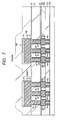
- FIG. 7 is a sectional view of the same regions as illustrated in FIG. 6 in a step subsequent to the step illustrated in FIG. 6 ;
- FIG. 8 is a sectional view of the same regions in a step subsequent to the step illustrated in FIG. 7 ;
- FIG. 9 is a sectional view of the same regions in a step subsequent to the step illustrated in FIG. 8 ;
- FIG. 10 is a sectional view of the same regions in a step subsequent to the step illustrated in FIG. 9 ;
- FIG. 11 is a sectional view of the same regions in a step subsequent to the step illustrated in FIG. 10 ;
- FIG. 12 is a partial sectional view of a semiconductor device according to a second embodiment of the invention.
- FIG. 13 is a partial sectional view of upper-layer interconnections of a workpiece of the semiconductor device according to the second embodiment to illustrate a step in a method for manufacturing this device;
- FIG. 14 is a sectional view of the same regions as illustrated in FIG. 13 in a step subsequent to the step illustrated in FIG. 13 ;
- FIG. 15 is a sectional view of the same regions in a step subsequent to the step illustrated in FIG. 14 ;
- FIG. 16 is a partial sectional view of an example of a semiconductor device according to the third embodiment of the invention.
- FIG. 17 is a partial sectional view of another example of the semiconductor device according to a third embodiment.
- FIG. 18 is a partial sectional view of upper-layer interconnections in one out of element formation regions and a slit region adjacent to the region in an example of an interconnection structure investigated by the inventors before the present invention has been made.
- the present invention may be divided into plural sections or plural embodiments as the need arises, so as to be described in accordance with the sections or embodiments.
- these are not independently of each other; thus, any one thereof may be a modified example, details, a supplement for explanation, or some other of a part or the whole of the other or another except any case where it is evidently stated that such a matter is denied.
- the element-number or the other is not limited to the specific numerical value, and may be a numerical value above or below the specific numerical value except any case where it is evidently stated that this matter is denied, any case where the element-number or the other is theoretically limited to the specific numerical value, or some other case.
- any constituent, any process-constituting step, or the like is not necessarily essential except any case where it is evidently stated that this matter is denied, any case where the constituent or the other is theoretically essential, or some other case.
- an MISFET metal insulator semiconductor field effect transistor
- MIS metal insulator semiconductor field effect transistor
- the word “metal” denotes an electroconductor such as polycrystalline silicon as well as a metal
- the word “wafer” mainly denotes a silicon monocrystal wafer, and further denotes any SOI (silicon on insulator) wafer, any insulating film substrate on which an integrated circuit is to be formed, or some other.
- the shape thereof is not limited, and may be, for example, a circle, any shape equivalent to a circle, a square, or a rectangle.
- the word “silicon nitride” denotes Si 3 N 4 of course, and further denotes any nitride of silicon that has a composition similar to Si 3 N 4 .
- FIG. 18 is a sectional view of upper-layer interconnections in one out of element formation regions, and a slit region adjacent thereto in an example of the structure.
- an interconnection 51 of a top layer is comprised of the following three members: a conductive film 26 containing, for example, Al (aluminum) as a main conductive material, this film being to be referred to as the Al film 26 hereinafter; and TiN (titanium nitride) films 27 and 28 that are formed on the lower and upper surfaces of the film 26 , respectively, in order to improve the EM (electro-migration) resistance thereof.
- the TiN film 28 formed on the upper surface of the Al film 26 also has a function of an antireflection film.
- the top-layer interconnection 51 is covered with an insulating film 29 for bonding, and a first passivation film 30 .
- the bonding insulating film 29 is laid to prevent the first passivation film 30 from being peeled.
- the first passivation film 30 is comprised of, for example, a silicon oxide film 30 a formed by high-density plasma CVD, and a silicon nitride film 30 b formed by plasma CVD.
- the film 30 has a function as a protecting film for preventing the invasion of water or impurities from the outside, and restraining the penetration of ⁇ -rays.
- openings are made in the TiN film 28 as the top layer of the top-layer interconnection 51 , which is used for bonding pads BP, the bonding insulating film 29 , and the first passivation film 30 .
- the Al film 26 of the top-layer interconnection 51 is exposed to the bottom surface of the opening 31 .
- the upper surface of the first passivation film 30 and the side surface of the opening 31 are covered with a second passivation film 32 .
- the upper surface of the top-layer interconnection 51 used for the bonding pads BP is not covered with the second passivation film 32 , so as to be naked in order to couple the interconnection 51 with external terminals (such as bonding wires or bump).
- a guard ring (sealing) GR is formed to surround the element formation region.
- a slit (such as a trench or a trench pattern) SL is formed to surround the circumference of the guard ring GR.
- the inner walls of the slit SL are uncovered. Furthermore, this slit SL is made in the second passivation film 32 , the first passivation film 31 , the bonding insulating film 29 , and the interlayer dielectric 23 . However, by a variation in the precision in working for making the slit SL or some other factor, the slit SL may be made into a deeper position so that the bottom of the slit SL may reach a barrier insulating film 22 , a cap insulating film 20 a , and an insulating film 19 a for interconnection formation, each of which is below the interlayer dielectric 23 .
- the interconnection-forming insulating film 19 a is mainly a low-k film in order to make the parasitic capacitance of an interconnection to be formed small.
- the low-k film is poorer in humidity resistance than insulating films made of SiO 2 , so that the low-k film permits an easy invasion of water.
- the bottom of the slit SL can be located not to reach the interconnection-forming insulating film 19 a by forming the barrier insulating film 22 , which is laid between the interlayer dielectric 23 and the interconnection-forming insulating film 19 a , so as to have a large thickness.
- the barrier insulating film 22 is usually made of nitrogen-containing silicon, such as SiN (silicon nitride), SiCN (silicon carbonitride) or SiON (silicon oxynitride), and the dielectric constant thereof is higher than that of SiO 2 . For this reason, when the barrier insulating film 22 is made thick, the parasitic capacitance of the interconnection to be formed becomes large so that an element to be manufactured is hindered from being operated at a high speed.
- FIG. 1 is a partial sectional view of the semiconductor device
- FIG. 2 is a partial plan view of the device.
- a semiconductor device comprised of various desired semiconductor elements is formed in/over a main surface of a semiconductor substrate (semiconductor wafer worked in the form of a circular thin plate) made of a silicon monocrystal, so as to be assigned to each of divided semiconductor chips in the main surface.
- the semiconductor elements include CMOS (complementary metal oxide semiconductor) devices, resistance elements, and capacitance elements.
- CMOS devices are given as examples.
- a p-channel MISFET which configures a CMOS device is abbreviated as a pMIS
- an n-channel MISFT which configures a CMOS is abbreviated as an nMIS.
- an isolating region 2 made of an insulating film is formed in each element formation region of the semiconductor substrate 1 .
- a p well 3 is formed by ion-implanting a p-type conductive impurity into each first region of the semiconductor substrate 1
- an n well is formed by ion-implanting an n-type conductive impurity onto each second region, which is different from each of the first regions.
- Each nMIS is comprised of, for example, a gate insulating film 5 formed on the front surface of the semiconductor substrate 1 (the p well 3 ), a gate electrode 6 n formed on the gate insulating film 5 , a side wall 7 formed on the side surface of the gate electrode 6 n , and an n-type semiconductor region 8 which is formed in the semiconductor 1 (the p well 3 ) and at both sides of the gate electrode 6 n , and which functions as a source and a drain.
- each pMIS is comprised of, for example, the gate insulating film 5 formed on the front surface of the semiconductor substrate 1 (the p well 4 ), a gate electrode 6 p formed on the gate insulating film 5 , a side wall 7 formed on the side surface of the gate electrode 6 p , and a p-type semiconductor region 9 which is formed in the semiconductor 1 (the n well 4 ) and at both sides of the gate electrode 6 n , and which functions as a source and a drain.
- nMIS and pMIS are covered with an interlayer dielectric 10 .
- Coupling holes 11 are made in this interlayer dielectric 10 so as to reach required portions over the n-type semiconductor regions 8 , the p-type semiconductor regions 9 , and some other.
- a plug 12 is buried which is made of a conductive film containing W (tungsten) as a main conductive material.
- An interconnection M 1 of a first layer is formed to be coupled with the plug 12 .
- the first-layer interconnection M 1 is, for example, a conductive film containing Cu as a main conductive material, and is formed by the single damascene process.
- each interconnection trench 15 is made in a laminated film comprised of a stopper insulating film 13 and an insulating film 14 for interconnection formation, and the first-layer interconnection M 1 , which is a conductive film containing Cu as a main conductive material, is buried in the interconnection trench 15 .
- interconnections from an interconnection M 2 of a second layer to an interconnection M 6 of a sixth layer are each, for example, a conductive film containing Cu as a main conductive material, and are each formed by the dual damascene process.
- the sixth-layer interconnection M 6 is, for example, a patterned conductive film containing Al as a main conductive material.
- the interconnection M 6 is formed by working a conductive film containing Al as a main conductive material and deposited on the semiconductor substrate 1 by use of a resist pattern as a mask.
- the sixth-layer interconnection M 6 partially functions as bonding pads BP.
- the interconnections from the first- to the sixth-layer interconnections M 1 to M 6 are formed in each of the element formation regions, and are used for the operation of concerned circuits. Furthermore, as illustrated in FIG. 2 , a guard ring GR having a laminated structure comprised of the interconnections from the first- to the sixth-layer interconnections M 1 to M 6 is formed to surround each element formation region DA as each of the above-mentioned element formation regions. Furthermore, a slit SL is made to surround the guard ring GR. Specifically, the guard ring GR and the slit SL are formed between each of the element formation regions, and scribe lines 100 through which the semiconductor wafer is to be cut into semiconductor chips SC. In the first embodiment, the number of the interconnection layers is 6; however, the number of interconnection layers is not limited thereto.
- the second-layer interconnection M 2 is formed to be integrated with a coupling member for coupling the second-layer interconnection M 2 with the first-layer interconnection M 1 , which is laid beneath the interconnection M 2 .
- the second-layer interconnection M 2 and the coupling member which are integrated with each other so as to be formed as a conductive film containing Cu as a main conductive material, are buried in coupling holes 18 , which are made in a laminated film comprised of a stopper insulating film 16 and an interlayer dielectric 17 , and buried in interconnection trenches 21 , which are made in a laminated film comprised of an insulating film 19 for interconnection formation and a cap insulating film 20 .
- the stopper insulating film 16 is made of a material having a smaller etch rate than that of the material of the interlayer dielectric 17 , and is, for example, a silicon nitride film formed by plasma CVD. Furthermore, the stopper insulating film 16 has a function as a protecting film for preventing the diffusion of Cu comprised of the first-layer interconnection M 1 .
- the interlayer dielectric 17 is, for example, a TEOS (tetraethyl orthosilicate) film formed by plasma CVD.
- the interconnection-forming insulating film 19 is an insulating film having a lower dielectric constant than SiO 2 , and is, for example, a low-k film, which has a dielectric constant of 3.5 or less. The low-k film may be, for example, a fluorine-containing silicon oxide film.
- the cap insulating film 20 is, for example, a TEOS film formed by plasma CVD.
- the interconnections from the third to fifth interconnections M 3 to M 5 each have the same structure as the second-layer interconnection M 2 , and are successively formed upward over the second-layer interconnection M 2 .
- the fifth-layer interconnection M 5 is covered with a barrier insulating film 22 and an interlayer dielectric 23 .
- these films 22 and 23 coupling holes 24 which reach the fifth-layer interconnection M 5 are made.
- a plug 25 is buried which is made of a conductive film containing, for example, W as a main conductive material.
- the sixth-layer interconnection M 6 is formed to be coupled with the plugs 25 .
- the barrier insulating film 22 has a function as a protecting film for preventing the diffusion of Cu, and is, for example, a nitrogen-containing silicon film, such as a SiN film; a SiCN film or a SiON film.
- the thickness thereof is, for example, from about 175 to 225 nm.
- the interlayer dielectric 23 is, for example, a silicon oxide film formed by plasma CVD. The thickness thereof is, for example, about 1000 nm.
- the sixth-layer interconnection M 6 is made mainly of an Al film 26 , and TiN films 27 and 28 are formed on the lower and upper surfaces of the film 26 , respectively, in order to improve the EM resistance. Furthermore, the TiN film 28 formed on the upper surface of the Al film 26 also has a function of an antireflection film.
- the Al film 26 is formed by, for example, sputtering, and the thickness thereof is, for example, about 1000 nm.
- the TiN films 27 and 28 formed on the lower and upper surfaces of the Al film 26 , respectively, are each formed by, for example, sputtering.
- the thickness of the TiN film 28 formed on the upper surface of the Al film is, for example, from about 100 to 300 nm.
- the sixth-layer interconnection M 6 is covered with an insulating film 29 for bonding, and a first passivation film 30 .
- the bonding insulating film 29 is, for example, a silicon oxide film formed by plasma CVD, and is laid to prevent the first passivation film 30 from being peeled.
- the thickness thereof is, for example, about 70 nm.
- the first passivation film 30 is comprised of, for example, a silicon oxide film 30 a (lower-layer passivation film 30 A) formed by plasma CVD, and a silicon nitride film 30 b (upper-layer passivation film 30 B) formed by plasma CVD.
- the film 30 has a function as a protecting film for preventing the invasion of water and impurities from the outside and restraining the penetration of ⁇ -rays.
- the thickness of the silicon oxide film 30 a positioned as the lower layer of the passivation films is, for example, about 1000 nm, and that of the silicon nitride film 30 b positioned as the upper layer thereof is, for example, 600 nm.
- openings are made in the TiN film 28 as the top layer of the sixth-layer interconnection M 6 , which is used for bonding pads BP, the bonding insulating film 29 and the first passivation film 30 , and the Al film 26 of the sixth-layer interconnection M 6 is exposed to the bottom surface of the opening 31 .
- the slit SL is formed to surround the circumference of the guard ring GR.
- the slit SL is made in the interlayer dielectric 23 laid between the fifth-layer interconnection M 5 and the sixth-layer interconnection M 6 , the bonding insulating film 29 , and the first passivation 30 .
- the width of the slit SL is, for example, from about 4 to 5 nm. It is desired that the bottom of the slit SL does not penetrate completely through the interlayer dielectric 23 in the film thickness direction of this film 23 so that the bottom does not reach the barrier insulating film 22 , which is laid between the fifth-layer interconnection M 5 and the sixth-layer interconnection M 6 and functions as a protecting film for preventing the diffusion of Cu.
- the bottom of the slit SL may reach the barrier insulating film 22 .
- the slit SL it is sufficient for the slit SL that the following is not caused: the bottom of the slit SL penetrates through the barrier insulating film 22 in the film thickness direction of this film 22 to reach a cap insulating film 20 a (for example, an insulating film made of the same material as used for the cap insulating film 20 ) as a layer beneath the film 22 .
- an insulating film 19 a for interconnection formation (for example, an insulating film made of the same material as used for the interconnection-forming insulating film 19 ) contains fluorine so that the humidity resistance of this film 19 a is poorer than that of any insulating film containing no fluorine; therefore, if the bottom of the slit SL reaches the cap insulating film 20 a to further reach the interconnection-forming insulating film 19 a laid beneath the film 20 a , the invasion of water through the slit SL is easily caused so that the Cu interconnections formed in each of the element formation regions is corroded.
- an insulating film 19 a for interconnection formation contains fluorine so that the humidity resistance of this film 19 a is poorer than that of any insulating film containing no fluorine; therefore, if the bottom of the slit SL reaches the cap insulating film 20 a to further reach the interconnection-forming insulating film 19 a laid beneath the film 20 a , the invasion
- reference number 16 a represents a stopper insulating film made of the same material as used for the stopper insulating film 16 ; 17 a , an interlayer dielectric made of the same material as used for the interlayer dielectric 17 ; 18 a , coupling holes made in the same manner as used for making the coupling holes 18 ; and 21 a , interconnection trenches made in the same manner as used for making the interconnection trenches 21 .
- a second passivation film 32 covers the upper surface of the first passivation film 30 , the side surface of the opening 31 , which is made to make the upper surface of the sixth-layer interconnection M 6 naked (or uncovered), and the inner walls (the side surfaces and the bottom surface) of the slit SL, these surfaces being named or classified so when viewed from the above.
- the upper surface of the sixth-layer interconnection M 6 used for the bonding pads BP is not covered with the second passivation film 32 so as to be naked for the purpose of being coupled with external terminals (such as bonding wires or bumps).
- the second passivation film 32 is, for example, a silicon nitride film formed by plasma CVD, and the thickness thereof is, for example, from about 100 to 300 nm.
- the invasion of water into the concerned element formation region through the slit SL can be further prevented.
- the invasion of water can be prevented by the formation of the slit SL for causing the bottom thereof not to penetrate through the barrier insulating film 22 , and additionally the water-invasion can be further prevented by the covering of the inner walls (the side surfaces and the bottom surface) of the slit SL with the second passivation film 32 .
- the Cu interconnections are not corroded by the water-invasion into the element formation region through the slit SL, so that a fall in the reliability of the semiconductor device can be prevented.
- the side surface of the opening 31 made to make the upper surface of the sixth-layer interconnection M 6 used for the bonding pads BP naked is covered with the second passivation film 32 , and the TiN film 28 formed on the upper surface of the Al film 26 is not naked. Accordingly, this TiN film 28 is not easily oxidized so that the volume of the TiN film 28 is not easily expanded through oxidization. Thus, the first passivation film 30 , the interlayer dielectric 23 or some other is not cracked. In this manner, in a reliability test for the semiconductor device, the Cu interconnections are not corroded by the water-invasion into the element formation region through the slit SL, so that a fall in the reliability of the semiconductor device can be prevented.
- FIGS. 3 to 11 are each a partial sectional view of the semiconductor or a workpiece thereof.
- FIGS. 6 to 11 are, more specifically, each a partial sectional view illustrating upper-layer interconnections (corresponding to the above-mentioned fifth- and sixth-layer interconnections M 5 and M 6 ) of the semiconductor device or the workpiece.
- desired semiconductor elements are formed on/in a semiconductor substrate 1 (semiconductor wafer worked in the form of a circular thin plate) made of a silicon monocrystal.
- the illustrated semiconductor elements are CMOS devices as examples.
- an insulating region 2 made of an insulating film is formed in each element isolating region of a semiconductor substrate 1 , and then a p-type conductive impurity is ion-implanted into the semiconductor substrate 1 to make a p well 3 .
- an n-type conductive impurity is ion-implanted into the substrate 1 to make an n well 4 .
- a gate insulating film 5 and gate electrodes 6 n and 6 p which are to constitute an nMIS and pMIS, are formed, and further side walls 7 are formed onto side surfaces of the gate electrodes 6 n and 6 p .
- n-type conductive impurity is ion-implanted into the p well 3 and at both sides of the gate electrode 6 n so as to form n-type semiconductor regions 8 , which function as a source and a drain of the nMIS, respectively, in the manner of self-alignment with the gate electrode 6 n and concerned ones of the side walls 7 .
- a p-type conductive impurity is ion-implanted into the n well 4 and by both sides of the gate electrode 6 p so as to form p-type semiconductor regions 9 , which function as a source and a drain of the pMIS, respectively, in the manner of self-alignment with the gate electrode 6 p and concerned ones of the side walls 7 .
- multi-level interconnections are formed, through which the various semiconductor elements formed in/on the main surface of the semiconductor substrate 1 are electrically coupled with each other.
- a silicon nitride film is deposited onto the main surface of the semiconductor substrate 1 by CVD to form a lower-layer insulating film 10 a .
- a TEOS film is deposited onto the lower-layer insulating film 10 a by plasma CVD to form an upper-layer insulating film 10 b .
- an interlayer dielectric 10 is formed which is comprised of the lower-layer insulating film 10 a and the upper-layer insulating film 10 b .
- the front surface of the upper-layer insulating film 10 b is polished by CMP (chemical mechanical polishing).
- the polishing of the front surface of the upper-layer insulating film 10 b by the CMP makes the front surface of the interlayer dielectric 10 flat and smooth.
- a resist pattern is used as a mask to etch the interlayer dielectric 10 , so as to make, at predetermined positions, coupling holes 11 each reaching the source or the drain of the nMIS or the pMIS, or some other.
- a barrier metal film is formed over the main surface of the semiconductor substrate 1 .
- the barrier metal film is, for example, a Ti film or a TiN film.
- a metal film such as a W film is deposited onto the barrier metal film.
- the metal film and the barrier metal film are polished by, for example, CMP so as to bury the barrier metal film and the metal film into the coupling holes 11 . In this way, plugs 12 containing the metal film as a main conductive film are formed.
- the stopper insulating film 13 is a film which is to function as an etching stopper at the time of making interconnection trenches 15 in the interconnection-forming insulating film 14 .
- the stopper insulating film 13 is made of a material having a smaller etch rate than that of the material of the interconnection-forming insulating film 14 .
- the stopper insulating film 13 is, for example, a silicon nitride film formed by plasma CVD.
- the interconnection-forming insulating film 14 is, for example, a silicon oxide film formed by plasma CVD.
- an interconnection M 1 of a first layer is formed by the damascene process.
- the interconnection trenches 15 are first made in predetermined regions of the stopper insulating film 13 and the interconnection-forming insulating film 14 by dry etching using a resist pattern as a pattern. Thereafter, a barrier metal film is formed over the main surface of the semiconductor substrate 1 .
- the barrier metal film is, for example, a TiN film, a Ta film or a TaN film.
- a Cu seed layer is formed on the barrier metal film by CVD or sputtering, and further an electroplating method is used to form a Cu plating layer on the Cu seed layer.
- the Cu plating layer is buried in the interconnection trenches 15 .
- the Cu plating film, the Cu seed layer and the barrier metal film are removed by, for example, CMP, so as to form, as the first-layer interconnection M 1 , an interconnection containing the Cu film as a main conductive film inside the interconnection trenches 15 .
- interconnections from second- to the fifth-layer interconnections M 2 to M 5 are formed by the dual damascene process.
- a stopper insulating film 16 , an interlayer dielectric 17 , an insulating film 19 for interconnection formation, and a cap insulating film 20 are successively formed over the main surface of the semiconductor substrate 1 .
- coupling holes 18 are to be made in the stopper insulating film 16 and the interlayer dielectric 17
- interconnection trenches 21 are to be made in the interconnection-forming insulating film 19 and the cap insulating film 20 .
- the stopper insulating film 16 is made of a material having a smaller etch rate than that of the material of the interlayer dielectric 17 , and is, for example, a silicon nitride film formed by plasma CVD. Furthermore, the stopper insulating film 16 has a function as a protecting film for preventing the diffusion of Cu comprised of the first-layer interconnection M 1 .
- the interlayer dielectric 17 is, for example, a TEOS film formed by plasma CVD.
- the interconnection-forming insulating film 19 is an insulating film having a lower dielectric constant than SiO 2 , and is, for example, a low-k film, which has a dielectric constant of 3.5 or less. The low-k film may be, for example, a fluorine-containing silicon oxide film.
- the cap insulating film 20 is, for example, a TEOS film formed by plasma CVD.
- the cap insulating film 20 , the interconnection-forming insulating film 19 , the interlayer dielectric 17 and the stopper insulating film 16 are successively worked by etching using, as a mask, a resist pattern for coupling-hole-formation.
- the stopper insulating film 16 functions as an etching stopper.
- the cap insulating film 20 and the interconnection-forming insulating film 19 are successively worked by etching using, as a mask, a resist pattern for interconnection-trench-formation. In this way, coupling holes 18 are made in the stopper insulating film 16 and the interlayer dielectric 17 , and further interconnection trenches 21 are made in the interconnection-forming insulating film 19 and the cap insulating film 20 .
- a second-layer interconnection M 2 is formed inside the coupling holes 18 and the interconnection trenches 21 .
- the second-layer interconnection M 2 is comprised of a barrier metal film, and a Cu film that is a main conductive film.
- a coupling member is formed to be integrated with the second-layer interconnection M 2 , this coupling member being a member for coupling the second-layer interconnection M 2 with the first-layer interconnection M 1 , which is an interconnection below the interconnection M 2 .
- a barrier metal film is formed over the main surface of the semiconductor substrate 1 , so that the metal film is also buried into the coupling holes 18 and the interconnection trenches 21 .
- the barrier metal film is, for example, a TiN film, a Ta film, or a TaN film.
- a Cu seed layer is formed on the barrier metal film by CVD or sputtering, and further an electroplating method is used to form a Cu plating layer on the Cu seed layer.
- the Cu plating layer is buried in the coupling holes 18 and the interconnection trenches 21 .
- the Cu plating film, the Cu seed layer and the barrier metal film are removed by, for example, CMP, so as to form, as the second-layer interconnection M 2 , an interconnection containing the Cu film as a main conductive film inside the interconnection trenches 21 .
- upper-layer interconnections i.e., interconnections from the third- to the fifth-layer interconnections M 3 to M 5 are further formed.
- a sixth-layer interconnection M 6 which is an interconnection of a top-layer, is formed.
- a barrier insulating film 22 and an interlayer dielectric 23 are successively formed over the main surface of the semiconductor substrate 1 .
- the barrier insulating film 22 has a function as a protecting film for preventing the diffusion of Cu, and is, for example, a nitrogen-containing silicon film, a SiCN film, or a SiON film.
- the thickness thereof is, for example, from about 175 to 225 nm.
- the interlayer dielectric 23 is, for example, a silicon oxide film formed by plasma CVD. The thickness thereof is, for example, about 1000 nm.
- a resist pattern is used as a mask to etch the interlayer dielectric 23 and the barrier insulating film 22 successively to make coupling holes 24 reaching the fifth-layer interconnection M 5 at predetermined positions.
- a barrier metal film is formed over the main surface of the semiconductor substrate 1 .
- the barrier metal is, for example, a Ti film or a TiN film.
- a metal film such as a W film is deposited onto the barrier metal film.
- the metal film and the barrier metal film are polished by, for example, CMP so as to bury the barrier metal film and the metal film into the coupling holes 24 . In this way, plugs 25 containing the metal film as a main conductive film are formed.
- a TiN film 27 , an Al film 26 and a TiN film 28 are successively formed over the main surface of the semiconductor substrate 1 .
- the TiN films 27 and 28 formed on the lower surface and the upper surface of the Al film 26 , respectively, have a function of improving the EM resistance. Furthermore, the TiN film 28 formed on the upper surface of the Al film 26 also has a function of an antireflection film.
- the Al film 26 is formed by, for example, sputtering, and the thickness thereof is, for example, about 1000 nm.
- the TiN films 27 and 28 formed on the lower and upper surfaces of the Al film 26 , respectively, are each formed by, for example, sputtering.
- the thickness of the TiN film 28 formed on the upper surface of the Al film is, for example, from about 100 to 300 nm.
- the TiN film 28 , the Al film 26 and the TiN film 27 are successively etched by etching using a resist pattern as a mask to form, as the sixth-layer interconnection M 6 , a laminated film of the TiN film 27 , the Al film 26 and the TiN film 28 .
- multiple bonding pads BP made of the sixth-layer interconnection M 6 are formed in the circumferential region of each of the element formation regions (corresponding to the regions DAn in FIG. 2 ) for semiconductor chips (corresponding to the chips SC therein).
- a guard ring GR is formed which is made of a laminate comprised of the interconnections from the first- to sixth-layer interconnections M 1 to M 6 .
- an insulating film 29 for bonding and a lower-layer passivation film 30 A are successively formed over the main surface of the semiconductor substrate 1 .
- the bonding insulating film 29 is, for example, a silicon oxide film formed by plasma CVD, and is laid to prevent the lower-layer passivation film 30 A from being peeled.
- the thickness thereof is, for example, about 70 nm.
- the lower-layer passivation layer 30 A is, for example, a silicon oxide film 30 a formed by high-density plasma CVD, and the thickness thereof is, for example, about 1000 nm.
- an upper-layer passivation film 30 B is formed on the lower-layer passivation film 30 A.
- the upper-layer passivation film 30 B is, for example, a silicon nitride film 30 b formed by plasma CVD, and the thickness thereof is, for example, about 600 nm.
- the first passivation film 30 which is comprised of the lower-layer passivation film 30 A and the upper-layer passivation film 30 B, has a function as a protecting film for preventing the invasion of water or impurities from the outside, and restraining the penetration of ⁇ -rays.
- etching using a resist pattern RP 1 as a mask is utilized to etch, in each of the element formation regions, the first passivation film 30 , and the TiN film 28 as the top layer of the sixth-layer interconnection M 6 used for the bonding pads BP successively.
- a slit region adjacent to the element formation region
- the first passivation film 30 , the bonding insulating film 29 and the interlayer dielectric 23 are successively etched.
- openings a typical example of which is an opening 31 , are made.
- the sixth-layer interconnection M 6 used for the bonding pads BP is naked, and further in the slit region, a slit SL is made.
- the slit SL in the slit region is formed in such a manner that the bottom thereof is located at a position where the slit SL is not permitted to penetrate through the interlayer dielectric 23 in the film thickness direction of this film 23 . Accordingly, the bottom of the slit SL does not penetrate through the barrier insulating film 22 in the film thickness direction of this film 22 .
- the Al film 26 of the sixth-layer interconnection M 6 is exposed to the bottom surface of the opening 31 .
- the TiN film 28 formed on the upper surface of the Al film 26 is also exposed to the side surface of the opening 31 .
- the depth thereof is varied by a variation in the precision in working for making the slit SL, or some other factor; thus, the bottom of the slit SL may reach the barrier insulating film 22 .
- the bottom of the slit SL is kept in the barrier insulating film 22 so that the slit SL does not penetrate through the barrier insulating film 22 .
- the following defects and other defects may be caused: the coverage of a second passivation film 32 which is to be formed in a subsequent step becomes bad; the covering performance of a resist used to work the second passivation film 32 becomes bad; and the resist remains partially without being removed.
- the second passivation film 32 (described just above) is formed over the main surface of the semiconductor substrate 1 .
- the second passivation film 32 is, for example, a silicon nitride film formed by plasma CVD, and the thickness thereof is, for example, from about 100 to 300 nm.
- the second passivation film 32 covers the upper surface of the first passivation film 30 , the inner walls (the side surface and the bottom surface) of the opening 31 for making the sixth-layer interconnection M 6 used for the bonding pads BP naked, and the inner walls (the side surfaces and the bottom surface) of the slit SL, these surfaces being named or classified so when viewed from the above.
- a resist pattern RP 2 is used to remove only the second passivation film 32 on the upper surface of the sixth-layer interconnection M 6 used for the bonding pads BP, thereby making the Al film 26 of the sixth-layer interconnection M 6 naked.
- the passivation film 32 on the side surface of the opening 31 is not removed and the TiN film 28 is covered with the second passivation film 32 .
- the covering of the TiN film 28 with the second passivation film 32 makes it uneasy to oxidize the TiN film 28 so that an expansion in the volume of the TiN film 28 through oxidization is not easily caused.
- the first passivation film 30 , the interlayer dielectric 23 , and so on are not cracked so that the invasion of water through cracks can be prevented.
- a corrosion of the Cu interconnections in each of the element formation regions can be prevented.
- the second passivation film 32 formed on the inner walls (the side surfaces and the bottom surface) of the slit SL is not removed, either. In this way, the invasion of water through the slit SL can be prevented. Thus, a corrosion of the Cu interconnections in the element formation region can be prevented.
- the slit SL is formed to cause the bottom of the slit SL not to penetrate through the barrier insulating film 22 , and subsequently the inner walls (the side surfaces and the bottom surface) of the slit SL are covered with the second passivation film 32 .
- the side surface of the opening 31 which is made to make the upper surface of the sixth-layer interconnection M 6 used for the bonding pads BP naked, is covered with the second passivation film 32 , thereby preventing the TiN film 28 formed on the upper surface of the Al film 26 from being made naked, so as to prevent the first passivation film 30 , the interlayer dielectric 23 , and so on from being cracked by an expansion in the volume of the TiN film 28 through oxidization.
- the inner walls (the side surfaces and the bottom surface) of the slit SL made to surround the circumference of the guard ring GR are covered with the second passivation film 32 , thereby preventing water from invading the element formation region through the slit SL.
- the side surface of the opening 31 which is made to make the upper surface of the sixth-layer interconnection M 6 used for the bonding pads BP naked, is covered with the second passivation film 32 , thereby preventing the TiN film 28 from being made naked, so as to prevent the first passivation film 30 from being cracked by an expansion in the volume of the TiN film 28 through oxidization. In this way, the invasion of water into the element formation region through cracks is prevented.
- a sixth-layer interconnection which is an interconnection of a top layer is covered with a first passivation film in the same way as in the first embodiment; however, the second embodiment is different from the first embodiment in the following: the inner walls (the side surfaces and the bottom surface) of each slit made to surround the circumference of a guard ring, and the side surface of each opening made to make the upper surface of the sixth-layer interconnection used for bonding pads naked are covered with an upper-layer passivation film which configures an upper-layer region of the first passivation film.
- FIG. 12 is a partial sectional view of the semiconductor device and illustrates upper-layer interconnections (equivalent to the above-mentioned fifth- and sixth-layer interconnections M 5 and M 6 ) of this semiconductor device.
- Various semiconductor elements formed in/over a main surface of a semiconductor substrate 1 , and the structure of interconnections from a first-layer interconnection M 1 to the sixth-layer interconnection M 6 of the present device are the same as described in the first embodiment. Thus, a description thereof is omitted.
- the sixth-layer interconnection M 6 is covered with an insulating film 29 for bonding, and a first passivation film 30 .
- the bonding insulating film 29 is, for example, a silicon oxide film formed by plasma CVD, and is laid to prevent the first passivation film 30 from being peeled.
- the thickness thereof is, for example, about 70 nm.
- the first passivation film 30 is a laminated film comprised of a lower-layer passivation film 30 A and an upper-layer passivation film 30 B.
- the lower-layer passivation layer 30 A is, for example, a silicon oxide film 30 a formed by high-density plasma CVD.
- the upper-layer passivation film 30 B is a protecting film having a function of preventing the invasion of water, and is, for example, a silicon nitride film 30 b formed by plasma CVD.
- the thickness of the lower-layer passivation film 30 A is, for example, about 1000 nm.
- the thickness of the upper-layer passivation film 30 B is, for example, about 600 nm.
- the first passivation film 30 has a function as a protecting film for preventing the invasion of water or impurities from the outside, and restraining the penetration of ⁇ -rays.
- openings are made in a TiN film 28 as the top layer of the sixth-layer interconnection M 6 used for the bonding pads BP, the bonding insulating film 29 , and the lower-layer passivation film 30 A.
- An Al film 26 of the sixth-layer interconnection M 6 is exposed to the bottom surface of the opening 31 .
- a guard ring GR is formed to surround the circumference of the element formation region.
- a slit SL is made to surround the circumference of the guard ring GR.
- This slit SL is made in an interlayer dielectric 23 laid between the fifth- and the sixth-layer interconnections M 5 and M 6 , the bonding insulating film 29 , and the lower-layer passivation film 30 A.
- the bottom of the slit SL does not penetrate through the interlayer dielectric 23 in the film thickness direction of this film 23 , so as not to reach a barrier insulating film 22 which is laid between the fifth- and the sixth-layer interconnections M 5 and M 6 , and which has a function as a protecting film for preventing the diffusion of Cu.
- the width of the slit SL is, for example, from about 4 to 5 nm.
- the upper-layer passivation film 30 B covers the upper surface of the lower-layer passivation film 30 A, the side surface of the opening 31 made to make the upper surface of the sixth-layer interconnection M 6 used for the bonding pads BP naked, and the inner walls (the side surfaces and the bottom surface) of the slit SL, these surfaces being named or classified so when viewed from the above. Only the upper surface of the sixth-layer interconnection M 6 used for the bonding pads BP is not covered with the upper-layer passivation film 30 B, and is made naked in order to be coupled with external terminals (such as bonding wires or bumps).
- the inner walls (the side surfaces and the bottom surface) of the slit SL with the upper-layer passivation film 30 B, water from the outside can be prevented from invading the element formation region through the slit SL.
- the side surface of the opening 31 which is made to make the upper surface of the sixth-layer interconnection M 6 used for the bonding pads BP naked, with the upper-layer passivation film 30 B, the first passivation film 30 , the interlayer dielectric 23 and so on can be prevented from being cracked by an oxidization-caused expansion in the volume of the TiN film 28 .
- the invasion of water into the element formation region through cracks can be prevented.
- FIGS. 13 to 15 are each a partial sectional view illustrating upper-layer interconnections (equivalent to the above-mentioned fifth- and sixth-layer interconnections M 5 and M 6 ) of this semiconductor device or a workpiece thereof. Steps of forming various semiconductor elements in/over a main surface of a semiconductor substrate 1 , and then forming interconnections from a first-layer interconnection M 1 to a sixth-layer interconnection M 6 of the present device are the same as described about the first embodiment. Thus, a description thereof is omitted.
- etching using a resist pattern RP 3 as a mask is utilized to etch the lower-layer passivation film 30 A on the upper surface of the sixth-layer interconnection M 6 used for bonding pads BP, the bonding insulating film 29 and the TiN film 28 successively.
- etching using a resist pattern RP 3 as a mask is utilized to etch the lower-layer passivation film 30 A on the upper surface of the sixth-layer interconnection M 6 used for bonding pads BP, the bonding insulating film 29 and the TiN film 28 successively.
- the lower-layer passivation film 30 A, the bonding insulating film 29 , and the interlayer dielectric 23 are successively etched.
- openings a typical example of which is an opening 31 , are made through which the sixth-layer interconnection M 6 used for the bonding pads BP is naked.
- a slit SL which does not reach the barrier insulating film 22 is made.
- the Al film 26 which partially configures the sixth-layer interconnection M 6 is exposed to the bottom surface of the opening 31 .
- the TiN film 28 formed on the upper surface of the Al film 26 is also exposed to the side surface of the opening 31 .
- the depth thereof is varied by a variation in the precision of working for making the slit SL, or some other factor.
- the slit SL is formed in such a manner that the bottom thereof is kept in the barrier insulating film 22 so that the slit SL does not penetrate through the barrier insulating film 22 .
- an upper-layer passivation film 30 B is formed on the lower-layer passivation film 30 A.
- the upper-layer passivation film 30 B is a protecting film having a function of preventing the invasion of water, and is, for example, a silicon nitride film formed by plasma CVD. The thickness thereof is, for example, about 600 nm.
- the upper-layer passivation film 30 B covers the upper surface of the lower-layer passivation film 30 A, the inner walls (the side surface and the bottom surface) of the opening 31 made to make the sixth-layer interconnection M 6 used for the bonding pads BP naked, and the inner walls (the side surfaces and the bottom surface) of the slit SL, these surfaces being named or classified so when viewed from the above.
- a resist pattern RP 4 is used as a mask to remove only the upper-layer passivation film 30 B on the upper surface of the sixth-layer interconnection M 6 used for the bonding pads BP, thereby making the Al film 26 of the sixth-layer interconnection M 6 naked.
- the upper-layer passivation film 30 B on the side surface of the opening 31 is not removed and the TiN film 28 exposed to the side surface of the opening 31 is covered with the upper-layer passivation film 30 B.
- the covering of the TiN film 28 with the upper-layer passivation film 30 B makes it uneasy to oxidize the TiN film 28 so that an expansion in the volume of the TiN film 28 through oxidization is not easily caused.
- the first passivation film 30 , the interlayer dielectric 23 , and so on are not cracked so that the invasion of water through cracks can be prevented.
- a corrosion of the Cu interconnections in the element formation region can be prevented.
- the upper-layer passivation film 30 B formed on the inner walls (the side surfaces and the bottom surface) of the slit SL is not removed, either. In this way, the invasion of water through the slit SL can be prevented. Thus, a corrosion of the Cu interconnections in the element formation region can be prevented.
- the invasion of water into the element formation region from the outside can be prevented so that the same advantageous effects as manufactured by the first embodiment can be obtained.
- the second passivation film 32 is formed; however, in the second embodiment, the second passivation film 32 is not formed.
- material costs therefor can be made lower and the manufacturing period can be made shorter than in the first embodiment.
- a semiconductor device according to present the third embodiment is described with reference to FIGS. 16 and 17 .
- FIG. 16 is a partial sectional view of this device example and illustrates upper-layer interconnections (corresponding to the above-mentioned fifth- and sixth-layer interconnections M 5 and M 6 ) in an element formation region and a slit region of the device example.
- a sixth-layer interconnection M 6 is covered with an insulating film 29 for bonding, and a first passivation film 30 .
- the bonding insulating film 29 is, for example, a silicon oxide film formed by plasma CVD, and is laid to prevent the first passivation film 30 from being peeled.
- the thickness thereof is, for example, about 70 nm.
- the first passivation film 30 is a laminated film comprised of a lower-layer passivation film 30 a and an upper-layer passivation film 30 b .
- the lower-layer passivation layer 30 a is, for example, a silicon oxide film formed by high-density plasma CVD.
- the upper-layer passivation film 30 b is a protecting film having a function of preventing the invasion of water, and is, for example, a silicon nitride film formed by plasma CVD.
- the thickness of the lower-layer passivation film 30 a is, for example, about 1000 nm.
- the thickness of the upper-layer passivation film 30 b is, for example, about 600 nm.
- the first passivation film 30 has a function as a protecting film for preventing the invasion of water or impurities from the outside, and restraining the penetration of ⁇ -rays.
- openings are made in a TiN film 28 as the upper layer of the sixth-layer interconnection M 6 used for the bonding pads BP, the bonding insulating film 29 , and the lower-layer passivation film 30 a .
- An Al film 26 of the sixth-layer interconnection M 6 is exposed to the bottom surface of the opening 31 .
- a guard ring GR is formed to surround the circumference of the element formation region.
- a slit SL is made to surround the circumference of the guard ring GR.
- This slit SL is made in an interlayer dielectric 23 laid between the fifth- and the sixth-layer interconnections M 5 and M 6 , the bonding insulating film 29 , and the lower-layer passivation film 30 a .
- the bottom of the slit SL does not penetrate through the interlayer dielectric 23 in the film thickness direction of this film 23 , so as not to reach a barrier insulating film 22 which is laid between the fifth- and the sixth-layer interconnections M 5 and M 6 , and which has a function as a protecting film for preventing the diffusion of Cu.
- the width of the slit SL is, for example, from about 4 to 5 nm.
- FIG. 17 is a partial sectional view of this device example and illustrates upper-layer interconnections (corresponding to the above-mentioned fifth- and sixth-layer interconnections M 5 and M 6 ) in an element formation region and a slit region of the device example.
- the semiconductor device of this example has the same upper-layer interconnection structure as illustrated in FIG. 16 .
- a second passivation film 32 covers the upper surface of a first passivation film 30 , the side surfaces of openings, a typical example of which is an opening 31 , that are made (in the element formation region) to make the upper surface of a sixth-layer interconnection M 6 used for bonding pads BP naked, and the inner walls (the side surfaces and the bottom surface) of a slit SL, these surfaces being named or classified so when viewed from the above. Only the upper surface of the sixth-layer interconnection M 6 used for the bonding pads BP is not covered with the second passivation film 32 , and is made naked in order to be coupled with external terminals (such as bonding wires or bumps).
- the bottom of the slit SL does not penetrate the interlayer dielectric 23 in the film thickness direction of this film 23 so as not to reach the interconnection-forming insulating film 19 a .
- the invasion of water into the element formation region through the slit SL can be prevented.
- the invention may be applied to a semiconductor device having a slit (such as a trench or a trench pattern) made over a main surface of a semiconductor substrate so as to surround each element formation region, in order to prevent its interlayer dielectric, its interconnections and so on from being peeled.
- a slit such as a trench or a trench pattern
Landscapes
- Internal Circuitry In Semiconductor Integrated Circuit Devices (AREA)
- Metal-Oxide And Bipolar Metal-Oxide Semiconductor Integrated Circuits (AREA)
Abstract
Description
- Patent document 1: Japanese Unexamined Patent Publication No. 2007-115988
- Patent document 2: Japanese Unexamined Patent Publication No. 2006-140404
Claims (13)
Applications Claiming Priority (2)
| Application Number | Priority Date | Filing Date | Title |
|---|---|---|---|
| JP2010103362A JP5622433B2 (en) | 2010-04-28 | 2010-04-28 | Semiconductor device and manufacturing method thereof |
| JP2010-103362 | 2010-04-28 |
Publications (2)
| Publication Number | Publication Date |
|---|---|
| US20110266679A1 US20110266679A1 (en) | 2011-11-03 |
| US8513808B2 true US8513808B2 (en) | 2013-08-20 |
Family
ID=44857601
Family Applications (1)
| Application Number | Title | Priority Date | Filing Date |
|---|---|---|---|
| US13/095,735 Active 2031-06-28 US8513808B2 (en) | 2010-04-28 | 2011-04-27 | Semiconductor device having trench-isolated element formation region |
Country Status (2)
| Country | Link |
|---|---|
| US (1) | US8513808B2 (en) |
| JP (1) | JP5622433B2 (en) |
Cited By (2)
| Publication number | Priority date | Publication date | Assignee | Title |
|---|---|---|---|---|
| US20150001592A1 (en) * | 2013-06-28 | 2015-01-01 | Taiwan Semiconductor Manufacturing Co., Ltd. | Semiconductor Device With Self-Protecting Fuse And Method Of Fabricating The Same |
| US11075181B2 (en) | 2018-09-17 | 2021-07-27 | Samsung Electronics Co., Ltd. | Semiconductor device |
Families Citing this family (24)
| Publication number | Priority date | Publication date | Assignee | Title |
|---|---|---|---|---|
| JP5357401B2 (en) * | 2007-03-22 | 2013-12-04 | ルネサスエレクトロニクス株式会社 | Semiconductor device and manufacturing method thereof |
| KR101616044B1 (en) * | 2009-07-03 | 2016-04-28 | 삼성전자주식회사 | Semiconductor device comprising landing pad formed by electroless plating |
| JP5487469B2 (en) * | 2010-03-29 | 2014-05-07 | ルネサスエレクトロニクス株式会社 | Manufacturing method of semiconductor device |
| JP2012209287A (en) * | 2011-03-29 | 2012-10-25 | Renesas Electronics Corp | Semiconductor device and method of manufacturing semiconductor device |
| JP2013123000A (en) | 2011-12-12 | 2013-06-20 | Sony Corp | Solid-state image pickup device and method for manufacturing the same |
| JP2013197113A (en) * | 2012-03-15 | 2013-09-30 | Sony Corp | Solid-state imaging device and camera system |
| US9312204B2 (en) * | 2013-09-27 | 2016-04-12 | Intel Corporation | Methods of forming parallel wires of different metal materials through double patterning and fill techniques |
| TW201724510A (en) * | 2015-05-15 | 2017-07-01 | 西凱渥資訊處理科技公司 | RF isolation using substrate openings |
| US9536832B1 (en) * | 2015-12-30 | 2017-01-03 | International Business Machines Corporation | Junctionless back end of the line via contact |
| JP6443362B2 (en) * | 2016-03-03 | 2018-12-26 | 株式会社デンソー | Semiconductor device |
| CN107887285A (en) | 2016-09-30 | 2018-04-06 | 中芯国际集成电路制造(北京)有限公司 | Welding pad structure and its manufacture method and imaging sensor |
| JP6872991B2 (en) * | 2017-06-29 | 2021-05-19 | ルネサスエレクトロニクス株式会社 | Semiconductor devices and their manufacturing methods |
| KR102668080B1 (en) * | 2018-07-24 | 2024-05-22 | 삼성전자주식회사 | A semiconductor device |
| KR102704110B1 (en) * | 2019-08-09 | 2024-09-06 | 삼성전자주식회사 | Semiconductor devices including a thick metal layer and a bump |
| KR102807501B1 (en) * | 2019-10-02 | 2025-05-16 | 삼성전자주식회사 | Semiconductor devices including a thick metal layer |
| JP7465120B2 (en) * | 2020-03-10 | 2024-04-10 | キヤノン株式会社 | Semiconductor device, its manufacturing method and equipment |
| JP7378335B2 (en) * | 2020-03-31 | 2023-11-13 | エイブリック株式会社 | Semiconductor device and its manufacturing method |
| US11450624B2 (en) | 2020-05-29 | 2022-09-20 | Sandisk Technologies Llc | Semiconductor die including diffusion barrier layers embedding bonding pads and methods of forming the same |
| US11444039B2 (en) | 2020-05-29 | 2022-09-13 | Sandisk Technologies Llc | Semiconductor die including diffusion barrier layers embedding bonding pads and methods of forming the same |
| US12438105B2 (en) * | 2021-07-29 | 2025-10-07 | Taiwan Semiconductor Manufacturing Company, Ltd. | Seal ring structure and method of fabricating the same |
| US12154869B2 (en) * | 2022-03-23 | 2024-11-26 | Taiwan Semiconductor Manufacturing Company, Ltd. | Semiconductor package with high density of through-silicon vias (TSV) |
| WO2024080192A1 (en) * | 2022-10-12 | 2024-04-18 | ソニーセミコンダクタソリューションズ株式会社 | Semiconductor device, method for manufacturing semiconductor device, and optical detection device |
| KR20250034642A (en) * | 2023-09-04 | 2025-03-11 | 삼성전자주식회사 | Semiconductor devices and semiconductor packages having the same |
| WO2025220223A1 (en) * | 2024-04-19 | 2025-10-23 | 三菱電機モビリティ株式会社 | Semiconductor device, pressure sensor device, fuel cell system, and method for manufacturing semiconductor device |
Citations (10)
| Publication number | Priority date | Publication date | Assignee | Title |
|---|---|---|---|---|
| US20010045651A1 (en) * | 2000-05-08 | 2001-11-29 | Tatsuyuki Saito | Semiconductor integrated circuit device and a method of manufacturing the same |
| US6677679B1 (en) * | 2001-02-06 | 2004-01-13 | Advanced Micro Devices, Inc. | Use of SiO2/Sin for preventing copper contamination of low-k dielectric layers |
| US6849541B1 (en) * | 2003-12-19 | 2005-02-01 | United Microelectronics Corp. | Method of fabricating a dual damascene copper wire |
| US20060103025A1 (en) | 2004-11-15 | 2006-05-18 | Renesas Technology Corp. | Semiconductor device including sealing ring |
| JP2007115988A (en) | 2005-10-21 | 2007-05-10 | Renesas Technology Corp | Semiconductor device |
| US7285460B2 (en) * | 2002-08-30 | 2007-10-23 | Fujitsu Limited | Semiconductor device and method of manufacturing the same |
| US20100255675A1 (en) * | 2007-02-23 | 2010-10-07 | Fujitsu Microelectronics Limited | Semiconductor device and method for manufacturing the same |
| US20100327449A1 (en) * | 2006-01-13 | 2010-12-30 | Renesas Electronics Corporation | Semiconductor device and manufacturing method of semiconductor device |
| US20120038055A1 (en) * | 2008-03-21 | 2012-02-16 | Ching-Chung Ko | Power and ground routing of integrated circuit devices with improved ir drop and chip performance |
| US20120252205A1 (en) * | 2005-07-06 | 2012-10-04 | Renesas Electronics Corporation | Semiconductor device and a method of manufacturing the same |
Family Cites Families (5)
| Publication number | Priority date | Publication date | Assignee | Title |
|---|---|---|---|---|
| WO2004097916A1 (en) * | 2003-04-30 | 2004-11-11 | Fujitsu Limited | Method for fabricating semiconductor device, semiconductor wafer and semiconductor device |
| US7224060B2 (en) * | 2004-01-30 | 2007-05-29 | Chartered Semiconductor Manufacturing Ltd. | Integrated circuit with protective moat |
| JP2006303452A (en) * | 2005-03-25 | 2006-11-02 | Sanyo Electric Co Ltd | Semiconductor device and manufacturing method thereof |
| WO2008126268A1 (en) * | 2007-03-30 | 2008-10-23 | Fujitsu Microelectronics Limited | Semiconductor device |
| JP2009021528A (en) * | 2007-07-13 | 2009-01-29 | Toshiba Corp | Semiconductor device |
-
2010
- 2010-04-28 JP JP2010103362A patent/JP5622433B2/en active Active
-
2011
- 2011-04-27 US US13/095,735 patent/US8513808B2/en active Active
Patent Citations (13)
| Publication number | Priority date | Publication date | Assignee | Title |
|---|---|---|---|---|
| US20010045651A1 (en) * | 2000-05-08 | 2001-11-29 | Tatsuyuki Saito | Semiconductor integrated circuit device and a method of manufacturing the same |
| US6677679B1 (en) * | 2001-02-06 | 2004-01-13 | Advanced Micro Devices, Inc. | Use of SiO2/Sin for preventing copper contamination of low-k dielectric layers |
| US7285460B2 (en) * | 2002-08-30 | 2007-10-23 | Fujitsu Limited | Semiconductor device and method of manufacturing the same |
| US20100140743A1 (en) * | 2002-08-30 | 2010-06-10 | Fujitsu Limited | Semiconductor device and method of manufacturing the same |
| US6849541B1 (en) * | 2003-12-19 | 2005-02-01 | United Microelectronics Corp. | Method of fabricating a dual damascene copper wire |
| US20060103025A1 (en) | 2004-11-15 | 2006-05-18 | Renesas Technology Corp. | Semiconductor device including sealing ring |
| JP2006140404A (en) | 2004-11-15 | 2006-06-01 | Renesas Technology Corp | Semiconductor device |
| US20120252205A1 (en) * | 2005-07-06 | 2012-10-04 | Renesas Electronics Corporation | Semiconductor device and a method of manufacturing the same |
| US20120248613A1 (en) * | 2005-07-06 | 2012-10-04 | Renesas Electronics Corporation | Semiconductor device and a method of manufacturing the same |
| JP2007115988A (en) | 2005-10-21 | 2007-05-10 | Renesas Technology Corp | Semiconductor device |
| US20100327449A1 (en) * | 2006-01-13 | 2010-12-30 | Renesas Electronics Corporation | Semiconductor device and manufacturing method of semiconductor device |
| US20100255675A1 (en) * | 2007-02-23 | 2010-10-07 | Fujitsu Microelectronics Limited | Semiconductor device and method for manufacturing the same |
| US20120038055A1 (en) * | 2008-03-21 | 2012-02-16 | Ching-Chung Ko | Power and ground routing of integrated circuit devices with improved ir drop and chip performance |
Cited By (6)
| Publication number | Priority date | Publication date | Assignee | Title |
|---|---|---|---|---|
| US20150001592A1 (en) * | 2013-06-28 | 2015-01-01 | Taiwan Semiconductor Manufacturing Co., Ltd. | Semiconductor Device With Self-Protecting Fuse And Method Of Fabricating The Same |
| US9070687B2 (en) * | 2013-06-28 | 2015-06-30 | Taiwan Semiconductor Manufacturing Co., Ltd. | Semiconductor device with self-protecting fuse |
| US9299658B2 (en) | 2013-06-28 | 2016-03-29 | Taiwan Semiconductor Manufacturing Co., Ltd. | Semiconductor device with self-protecting fuse and method of fabricating the same |
| US10014251B2 (en) | 2013-06-28 | 2018-07-03 | Taiwan Semiconductor Manufacturing Co., Ltd. | Semiconductor device with self-protecting fuse and method of fabricating the same |
| US11075181B2 (en) | 2018-09-17 | 2021-07-27 | Samsung Electronics Co., Ltd. | Semiconductor device |
| US11626377B2 (en) | 2018-09-17 | 2023-04-11 | Samsung Electronics Co., Ltd. | Semiconductor device |
Also Published As
| Publication number | Publication date |
|---|---|
| JP5622433B2 (en) | 2014-11-12 |
| US20110266679A1 (en) | 2011-11-03 |
| JP2011233746A (en) | 2011-11-17 |
Similar Documents
| Publication | Publication Date | Title |
|---|---|---|
| US8513808B2 (en) | Semiconductor device having trench-isolated element formation region | |
| US20250311462A1 (en) | 3dic seal ring structure and methods of forming same | |
| US9105706B2 (en) | Semiconductor device fabrication method capable of scribing chips with high yield | |
| TWI389254B (en) | Semiconductor integrated circuit device and manufacturing method of semiconductor integrated circuit device | |
| JP5324822B2 (en) | Semiconductor device | |
| US6998712B2 (en) | Semiconductor device and method for manufacturing the same | |
| US8420528B2 (en) | Manufacturing method of a semiconductor device having wirings | |
| US8247902B2 (en) | Semiconductor device and manufacturing method of the same | |
| JP4360881B2 (en) | Semiconductor device including multilayer wiring and manufacturing method thereof | |
| KR101369361B1 (en) | Semiconductor device having one body type crack stop structure | |
| US20060145347A1 (en) | Semiconductor device and method for fabricating the same | |
| US8481425B2 (en) | Method for fabricating through-silicon via structure | |
| US20100244199A1 (en) | Semiconductor device and method for manufacturing semiconductor device | |
| KR20090004469A (en) | Semiconductor devices | |
| JP4050876B2 (en) | Semiconductor integrated circuit device and manufacturing method thereof | |
| US20090189250A1 (en) | Semiconductor Device and a Method of Manufacturing the Same | |
| US9721883B1 (en) | Integrated circuit and manufacturing method thereof | |
| JP4891296B2 (en) | Manufacturing method of semiconductor integrated circuit device |
Legal Events
| Date | Code | Title | Description |
|---|---|---|---|
| AS | Assignment |
Owner name: RENESAS ELECTRONICS CORPORATION, JAPAN Free format text: ASSIGNMENT OF ASSIGNORS INTEREST;ASSIGNORS:HOTTA, KATSUHIKO;FURUSAWA, TAKESHI;MATSUI, TOSHIKAZU;AND OTHERS;REEL/FRAME:026575/0415 Effective date: 20110614 |
|
| STCF | Information on status: patent grant |
Free format text: PATENTED CASE |
|
| FEPP | Fee payment procedure |
Free format text: PAYOR NUMBER ASSIGNED (ORIGINAL EVENT CODE: ASPN); ENTITY STATUS OF PATENT OWNER: LARGE ENTITY |
|
| FPAY | Fee payment |
Year of fee payment: 4 |
|
| AS | Assignment |
Owner name: RENESAS ELECTRONICS CORPORATION, JAPAN Free format text: CHANGE OF ADDRESS;ASSIGNOR:RENESAS ELECTRONICS CORPORATION;REEL/FRAME:044928/0001 Effective date: 20150806 |
|
| MAFP | Maintenance fee payment |
Free format text: PAYMENT OF MAINTENANCE FEE, 8TH YEAR, LARGE ENTITY (ORIGINAL EVENT CODE: M1552); ENTITY STATUS OF PATENT OWNER: LARGE ENTITY Year of fee payment: 8 |
|
| MAFP | Maintenance fee payment |
Free format text: PAYMENT OF MAINTENANCE FEE, 12TH YEAR, LARGE ENTITY (ORIGINAL EVENT CODE: M1553); ENTITY STATUS OF PATENT OWNER: LARGE ENTITY Year of fee payment: 12 |