US8503496B2 - Device for judging state of semiconductor laser and method for judging state of semiconductor laser - Google Patents
Device for judging state of semiconductor laser and method for judging state of semiconductor laser Download PDFInfo
- Publication number
- US8503496B2 US8503496B2 US13/094,968 US201113094968A US8503496B2 US 8503496 B2 US8503496 B2 US 8503496B2 US 201113094968 A US201113094968 A US 201113094968A US 8503496 B2 US8503496 B2 US 8503496B2
- Authority
- US
- United States
- Prior art keywords
- semiconductor laser
- frequency
- electric current
- differential resistance
- state
- Prior art date
- Legal status (The legal status is an assumption and is not a legal conclusion. Google has not performed a legal analysis and makes no representation as to the accuracy of the status listed.)
- Expired - Fee Related, expires
Links
Images


Classifications
-
- H—ELECTRICITY
- H01—ELECTRIC ELEMENTS
- H01S—DEVICES USING THE PROCESS OF LIGHT AMPLIFICATION BY STIMULATED EMISSION OF RADIATION [LASER] TO AMPLIFY OR GENERATE LIGHT; DEVICES USING STIMULATED EMISSION OF ELECTROMAGNETIC RADIATION IN WAVE RANGES OTHER THAN OPTICAL
- H01S5/00—Semiconductor lasers
- H01S5/0014—Measuring characteristics or properties thereof
- H01S5/0021—Degradation or life time measurements
Definitions
- the embodiments discussed herein are related to a device for judging a state of a semiconductor laser and a method for judging a state of a semiconductor laser.
- a semiconductor laser Laser Diode, LD
- PD Photo Detector
- part of light emitted from a semiconductor laser is received by a PD, which detects a degree of deterioration in optical power to predict a prospective failure.
- the above scheme using a PD is accomplished by an exterior circuit on which the PD is optically mounted, thereby increasing the costs.
- Patent Literature 1 For the above, there has been proposed a method of detecting a failure of a semiconductor laser by measuring the differential resistance of the semiconductor (e.g., see Patent Literature 1).
- the technique of Patent Literature 1 compares a differential resistance obtained by monitoring and a differential resistance threshold for judging a failure in order to judge a prospective failure (deterioration).
- Patent Literature 1 unstably measures a differential resistance of a semiconductor laser, which may result in a large variation of the measured differential resistance.
- a differential resistance varies for each individual semiconductor laser, which requires a modification of a value of the judgment.
- an apparatus includes a device for judging a state of a semiconductor laser, the device including: a providing unit that provides a driving electric current to the semiconductor laser, the electric current being superimposed a first alternating current signal having a first frequency at a low side of an operational range of the semiconductor laser and a second alternating current signal having a second frequency different from the first frequency at a high side of the operational range; a first filter that extracts a first component corresponding to the first frequency from a voltage to be applied to the semiconductor laser; a second filter that extracts a second component corresponding to the second frequency from the voltage to be applied to the semiconductor laser; and a judge circuit that judges a state of the semiconductor laser based on a first differential resistance obtained from the result of the extracting by the first filter and a second differential resistance obtained from the result of the extracting by the second filter.
- a method includes a method for judging a state of a semiconductor, the method including: providing a driving electric current to the semiconductor laser, the electric current being superimposed a first alternative current signal having a first frequency at a Low side of an operational range of the semiconductor laser and a second alternating current signal having a second frequency different from the first frequency at a High side of the operational range; extracting a first component corresponding to the first frequency from voltage to be applied to the semiconductor laser; extracting a second component corresponding to the second frequency from the voltage to be applied to the semiconductor laser; and judging a state of the semiconductor laser based on a first differential resistance obtained from the extracted first component and a second differential resistance obtained from the extracted second component.
- FIG. 1 is a diagram illustrating a variation in differential resistance of a semiconductor laser
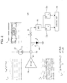
- FIG. 2 is a block diagram illustrating the entire configuration of a device for judging a state of a semiconductor laser according to a first embodiment
- FIG. 3 is a flow chart illustrating an example of a procedure of judging a state of a semiconductor laser
- FIG. 4 is a diagram illustrating an AC signal to be superimposed on a driving signal
- FIG. 5 is a diagram illustrating voltages corresponding to respective frequency components.
- FIG. 6 is a block diagram illustrating the entire configuration of a device for judging a state of a semiconductor laser according to a second embodiment.
- FIG. 1 is a diagram illustrating a variation in differential resistance of a semiconductor laser.
- the horizontal axis of a graph represents an operational electric current to be provided to a semiconductor laser; and the vertical axis of the graph represents a differential resistance of the semiconductor laser.
- the term “differential resistance” means a value obtained through differentiation on a resistance of a semiconductor laser.
- the solid line represents a differential resistance of a semiconductor laser in a normal state while the broken line represents a differential resistance of a semiconductor laser in an abnormal state (e.g., due to deterioration).
- the operational electric current provided to the semiconductor laser in a normal state comes to be the oscillation threshold I th (the oscillation threshold of a normal semiconductor laser)
- the differential resistance drastically declines so that light is emitted to generate laser oscillation.
- the differential resistance scarcely lowers. Accordingly, in a range of an electric current (the range of operation of the semiconductor laser) exceeding the oscillation threshold I th , the difference ⁇ Rd of the differential resistance against the operational electric current at the Low side from that at the High side is small.
- the semiconductor laser when the difference ⁇ Rd of the differential resistance exceeds a predetermined reference value ⁇ Rd ref , the semiconductor laser can be judged to be in an abnormal state. Conversely, when difference ⁇ Rd of the differential resistance does not exceed the predetermined reference value ⁇ Rd ref , the semiconductor laser can be judged to be in a normal state because the oscillation threshold is not larger than a predetermined value. Namely, the state of a semiconductor laser can be judged on the basis of the difference ⁇ Rd of the differential resistance.
- the state of a semiconductor laser can be determined on the basis of the ratio of a differential resistance at the Low side to a differential resistance at the High side. Specifically, when a ratio of the differential resistance at the Low side to the differential resistance at the High side is a predetermined value or more, the differential resistance at the Low side is relatively large to that of the High side. Accordingly, when the above ratio is larger than a predetermined value, the semiconductor laser can be judged to be in an abnormal state.
- a state of a semiconductor laser can be judged through the use of a parameter capable of judging whether or not the differential resistance at the Low side is relatively large to the differential resistance at the High side.
- FIG. 2 is a block diagram illustrating the entire configuration of the device 100 of the first embodiment.
- the device 100 includes a driver circuit 10 , a bias electric source 20 , an adder 30 , a semiconductor laser 40 , a resistor 50 , an ADC (Analog-to-Digital Convertor) 60 , digital filters 70 a and 70 b , and a judging unit 80 .
- the judging unit 80 may be a circuit, a FPGA (Field-Programmable Gate Array), or a processor.
- the driver circuit 10 generates and outputs a modulated electric current I mod , which varies with an input digital signal.
- the driver circuit 10 is direct-current coupled to the semiconductor laser 40 .
- the bias electric source 20 generates a bias electric current I bias that is to supply a bias electric current to the semiconductor laser 40 .
- the adder 30 adds the modulated electric current I mod and the bias electric current I bias to generate and output a driving electric current I LD to activate the semiconductor laser 40 .
- the semiconductor laser 40 has an oscillation threshold, and is exemplified by a direct-modulation Vertical Cavity Surface Emitting Laser (VCSEL).
- VCSEL Direct-modulation Vertical Cavity Surface Emitting Laser
- the resistor 50 has a predetermined resistance value.
- the ADC 60 converts an analog signal input via the resistor 50 into a digital signal, and outputs the digital signal to the digital filters 70 a and 70 b .
- the digital filters 70 a and 70 b function as a voltmeter that detects the voltage applied to the semiconductor laser 40 , and detect respective predetermined frequency components and output the components to the judging unit 80 .
- the judging unit 80 calculates a difference ⁇ Rd of a differential resistance at the Low side from a differential resistance at the High side of the semiconductor laser 40 on the basis of the frequency components input from the digital filters 70 a and 70 b.
- FIG. 3 is a flow diagram illustrating an example of a procedure of judging a state of the semiconductor laser 40 .
- the driver circuit 10 activates the semiconductor laser 40 in response to a digital signal input into the driver circuit 10 (step S 1 ).
- the first embodiment uses the driving electric current I LD on which an AC signal having a first frequency f L is superimposed for the Low side and an AC signal having a second frequency f H different from the first frequency f L is superimposed for the High side.
- the bias electric current I bias is exemplarily set as Formula (1) below.
- the modulated electric current I mod is exemplarily set as Formulae (2) and (3) below.
- “ ⁇ L ” represents an angular frequency corresponding to a first frequency f L
- ⁇ H represents an angular frequency corresponding to a second frequency f H .
- I bias I L sin ⁇ L t (1)
- I mod (at High) I H sin ⁇ H t ⁇ I L sin ⁇ L t (2)
- I mod (at Low) 0 (3)
- the driving electric current I LD has predetermined amplitudes at both High and Low sides.
- the voltage to be applied to the semiconductor laser 40 varies with the Low side and the High side of the driving electric current I LD .
- a variation in of the driving electric current I LD at the High side is presented by ⁇ I High ; and a variation in the driving electric current I LD at the Low side is presented by ⁇ I Low .
- the difference in voltage of the driving electric current I LD at the High side is represented by ⁇ V High ; and the difference in voltage of the driving electric current I LD that at the Low side is represented by ⁇ V Low .
- the differential resistance Rd Low obtained from the Low side of the driving electric current I LD is expressed by following Formula (4) while the differential resistance Rd High of the High side of the driving electric current I LD is expressed by following formula (5).
- Rd Low ⁇ V Low / ⁇ I Low
- Rd High ⁇ V High / ⁇ I High (5)
- the digital filter 70 a of the first embodiment is configured to extract the frequency component of the first frequency f L through spectral resolution; and the digital filter 70 b is configured to extract the frequency component of the second frequency f H through spectral resolution. Accordingly, the digital filters 70 a and 70 b detect voltages corresponding to the respective frequency components (step S 2 ) as illustrated in FIG. 5 . On the basis of the detected voltages V L and V H, and the amplitudes set for AC components of the High side and the Low side, the judging unit 80 calculates a differential resistance Rd Low at the Low side and a differential resistance RD High at the High side. The voltage V L represents one at the Low side and the voltage V H represents one at the High side.
- a predetermined threshold reference value ⁇ Rd ref
- the judging unit 80 judges the semiconductor laser 40 to be in an abnormal state (step S 4 ).
- the judging unit 80 judges the semiconductor laser 40 to be in a normal state (step S 5 ).
- the first embodiment calculates the difference of the differential resistances, it is possible to mitigate influence caused by inaccuracy in measuring the differential resistances.
- comparing the differential resistance of the semiconductor laser 40 in a normal state and the differential resistance of the semiconductor laser 40 when the measuring it is possible to mitigate variation in the differential resistance of each individual semiconductor laser. The above can improve the accuracy of judging the state of a semiconductor laser.
- the first embodiment can obtain the differential resistance while the semiconductor laser is operating, eliminating the requirement for stopping the operation of the semiconductor laser to judge the state thereof.
- the first frequency f L and the second frequency f H are preferably smaller than the frequency f signal of the digital signal of the driving electric current I LD .
- the AC signals of the first frequency f L and the second frequency f H preferably have amplitudes smaller than the modulation amplitude of the driving electric current I LD . These are because the influence of the AC signals of the first frequency f L and the second frequency f H can be suppressed on the driving electric current I LD .
- the Low side of the driving electric current I LD is preferably set to exceed the oscillation threshold I th of the semiconductor laser 40 in the normal state and to be less than an oscillation threshold of the semiconductor laser 40 being deteriorated.
- the oscillation threshold of the semiconductor laser 40 being deteriorated can be set beforehand.
- the High side of the driving electric current I LD is preferably set to exceed the above oscillation threshold of the semiconductor laser 40 being deteriorated.
- FIG. 6 is a block diagram illustrating the entire configuration of a device 100 a for judging a state of a semiconductor laser according to the second embodiment.
- the device 100 a is different from the device 100 of the first embodiment in the points that a capacitor 90 is disposed between the driver circuit 10 and the adder 30 and that the driver circuit 10 is alternating-current coupled to the semiconductor laser 40 .
- the bias electric current I bias is set to be constant, and an AC signal can be superimposed onto both Low side and High side of the modulation signal I mod in the driver circuit 10 .
- the driver circuit 10 and the bias electric source 20 functions as a driving electric current providing unit.
- the digital filter 70 a functions as a first filter that extracts the first frequency components while the digital filter 70 b functions as a second filter that extracts the second frequency components.
- the judging unit 80 functions as a judging unit that judges the state of the semiconductor laser.
- the judging unit 80 may be a circuit, a FPGA (Field-Programmable Gate Array), or a processor.
- a device for judging a state of a semiconductor laser and a method for judging a state of a semiconductor laser disclosed in the specification can improve the accuracy in judging a state of a semiconductor laser.
Landscapes
- Physics & Mathematics (AREA)
- Condensed Matter Physics & Semiconductors (AREA)
- General Physics & Mathematics (AREA)
- Electromagnetism (AREA)
- Optics & Photonics (AREA)
- Semiconductor Lasers (AREA)
- Testing Of Individual Semiconductor Devices (AREA)
Abstract
Description
- Patent Literature 1: Japanese Laid-open Patent Publication No. 2009-26889
I bias =I L sin ωL t (1)
I mod (at High)=I H sin ωH t−I L sin ωL t (2)
I mod (at Low)=0 (3)
Rd Low =ΔV Low /ΔI Low (4)
Rd High =ΔV High /ΔI High (5)
Claims (8)
Applications Claiming Priority (2)
| Application Number | Priority Date | Filing Date | Title |
|---|---|---|---|
| JP2010155265A JP5510135B2 (en) | 2010-07-07 | 2010-07-07 | Semiconductor laser determination apparatus and semiconductor laser determination method |
| JP2010-155265 | 2010-07-07 |
Publications (2)
| Publication Number | Publication Date |
|---|---|
| US20120008656A1 US20120008656A1 (en) | 2012-01-12 |
| US8503496B2 true US8503496B2 (en) | 2013-08-06 |
Family
ID=45438561
Family Applications (1)
| Application Number | Title | Priority Date | Filing Date |
|---|---|---|---|
| US13/094,968 Expired - Fee Related US8503496B2 (en) | 2010-07-07 | 2011-04-27 | Device for judging state of semiconductor laser and method for judging state of semiconductor laser |
Country Status (2)
| Country | Link |
|---|---|
| US (1) | US8503496B2 (en) |
| JP (1) | JP5510135B2 (en) |
Families Citing this family (1)
| Publication number | Priority date | Publication date | Assignee | Title |
|---|---|---|---|---|
| US10075257B2 (en) * | 2016-01-11 | 2018-09-11 | Nokia Of America Corporation | Optical spatial division multiplexing usable at short reach |
Citations (5)
| Publication number | Priority date | Publication date | Assignee | Title |
|---|---|---|---|---|
| JPS57187985A (en) * | 1981-05-15 | 1982-11-18 | Nippon Telegr & Teleph Corp <Ntt> | Gain stabilizing optical amplifier |
| JPH08111554A (en) | 1994-10-06 | 1996-04-30 | Fujitsu Ltd | Semiconductor laser control method and device |
| US5546221A (en) * | 1992-03-06 | 1996-08-13 | Fujitsu Limited | Optical amplifier apparatus |
| JP2009026889A (en) | 2007-07-18 | 2009-02-05 | Mitsubishi Electric Corp | Semiconductor laser device and method for avoiding operation stop of semiconductor laser device |
| US20100103971A1 (en) * | 2008-10-15 | 2010-04-29 | Han Wui Then | Optical bandwidth enhancement of light emitting and lasing transistor devices and circuits |
Family Cites Families (5)
| Publication number | Priority date | Publication date | Assignee | Title |
|---|---|---|---|---|
| JPS5970974A (en) * | 1982-10-15 | 1984-04-21 | Hitachi Ltd | Semiconductor laser deterioration detection device |
| US4680810A (en) * | 1985-06-28 | 1987-07-14 | American Telephone And Telegraph Company, At&T Bell Labs | Means for controlling a semiconductor device and communication system comprising the means |
| JPH10160785A (en) * | 1996-11-29 | 1998-06-19 | Nippon Telegr & Teleph Corp <Ntt> | Semiconductor laser sorting method and apparatus |
| JP3535002B2 (en) * | 1998-02-09 | 2004-06-07 | 日本電信電話株式会社 | Pass / fail judgment method of semiconductor laser |
| JP2005057069A (en) * | 2003-08-05 | 2005-03-03 | Matsushita Electric Ind Co Ltd | Semiconductor laser deterioration detection device, semiconductor laser device including the same, and semiconductor laser module assembly process |
-
2010
- 2010-07-07 JP JP2010155265A patent/JP5510135B2/en not_active Expired - Fee Related
-
2011
- 2011-04-27 US US13/094,968 patent/US8503496B2/en not_active Expired - Fee Related
Patent Citations (5)
| Publication number | Priority date | Publication date | Assignee | Title |
|---|---|---|---|---|
| JPS57187985A (en) * | 1981-05-15 | 1982-11-18 | Nippon Telegr & Teleph Corp <Ntt> | Gain stabilizing optical amplifier |
| US5546221A (en) * | 1992-03-06 | 1996-08-13 | Fujitsu Limited | Optical amplifier apparatus |
| JPH08111554A (en) | 1994-10-06 | 1996-04-30 | Fujitsu Ltd | Semiconductor laser control method and device |
| JP2009026889A (en) | 2007-07-18 | 2009-02-05 | Mitsubishi Electric Corp | Semiconductor laser device and method for avoiding operation stop of semiconductor laser device |
| US20100103971A1 (en) * | 2008-10-15 | 2010-04-29 | Han Wui Then | Optical bandwidth enhancement of light emitting and lasing transistor devices and circuits |
Also Published As
| Publication number | Publication date |
|---|---|
| JP2012018067A (en) | 2012-01-26 |
| JP5510135B2 (en) | 2014-06-04 |
| US20120008656A1 (en) | 2012-01-12 |
Similar Documents
| Publication | Publication Date | Title |
|---|---|---|
| US8275011B2 (en) | Optical transmission module, wavelength monitor, and wavelength drift detection method | |
| KR102132519B1 (en) | Device and method for controlling detection signal of lidar | |
| TWI674426B (en) | Open loop correction for optical proximity detectors | |
| TWI734677B (en) | Precision estimation for optical proximity detectors | |
| US9599651B2 (en) | Systems and methods of detecting ground faults in energy storage and/or generation systems that employ DC/AC power conversion systems | |
| US7427741B2 (en) | Bias control apparatus for avalanche photodiode and optical apparatus utilizing the bias control apparatus | |
| US9222810B1 (en) | In situ calibration of a light source in a sensor device | |
| US10825334B2 (en) | Smoke detector operational integrity verification system and method | |
| JP2013164263A (en) | Photo-receiving device, distance measurement device and shape measurement device | |
| US20170299901A1 (en) | Optical transmitter and optical transceiver | |
| US8503496B2 (en) | Device for judging state of semiconductor laser and method for judging state of semiconductor laser | |
| JP6439467B2 (en) | Optical signal quality monitoring device, optical signal quality monitoring method, and optical repeater | |
| KR101998859B1 (en) | Device and method for controlling detection signal of lidar | |
| US8450676B2 (en) | Optical receiver | |
| KR20160062587A (en) | Error detection apparatus and method of motor current sensor | |
| KR20150108133A (en) | Digital logic signal generating circuit for frequency measurement | |
| US20170288530A1 (en) | Power detection and transmission circuit coupling analog input signal on primary side to secondary side for power information calculation and related power supply apparatus | |
| KR20140058481A (en) | Glass surface pollution level measurement sensor which using reflected light for pollution estimate of pv module | |
| US10234501B2 (en) | Active noise suppression for optical voltage sensor | |
| JP2011096957A (en) | Method and apparatus for detection of fault in vcsel | |
| US9671283B1 (en) | Apparatus and method for modulating a laser beam and sensing the optical power thereof | |
| JP6111534B2 (en) | Optical measuring device and control method | |
| US20140185045A1 (en) | Etalon-based wavelegnth locking apparatus and alignment method | |
| FR3007843A1 (en) | METHOD AND DEVICE FOR DETERMINING THE PHASE OF AN ALTERNATIVE SIGNAL | |
| CN110296957B (en) | Method for operating an optical measuring system for measuring the concentration of a gas component in a measured gas |
Legal Events
| Date | Code | Title | Description |
|---|---|---|---|
| AS | Assignment |
Owner name: FUJITSU LIMITED, JAPAN Free format text: ASSIGNMENT OF ASSIGNORS INTEREST;ASSIGNOR:MATSUI, JUN;REEL/FRAME:026243/0875 Effective date: 20110316 |
|
| STCF | Information on status: patent grant |
Free format text: PATENTED CASE |
|
| FEPP | Fee payment procedure |
Free format text: PAYOR NUMBER ASSIGNED (ORIGINAL EVENT CODE: ASPN); ENTITY STATUS OF PATENT OWNER: LARGE ENTITY |
|
| FPAY | Fee payment |
Year of fee payment: 4 |
|
| FEPP | Fee payment procedure |
Free format text: MAINTENANCE FEE REMINDER MAILED (ORIGINAL EVENT CODE: REM.); ENTITY STATUS OF PATENT OWNER: LARGE ENTITY |
|
| LAPS | Lapse for failure to pay maintenance fees |
Free format text: PATENT EXPIRED FOR FAILURE TO PAY MAINTENANCE FEES (ORIGINAL EVENT CODE: EXP.); ENTITY STATUS OF PATENT OWNER: LARGE ENTITY |
|
| STCH | Information on status: patent discontinuation |
Free format text: PATENT EXPIRED DUE TO NONPAYMENT OF MAINTENANCE FEES UNDER 37 CFR 1.362 |
|
| FP | Lapsed due to failure to pay maintenance fee |
Effective date: 20210806 |