US8468410B2 - Address generation apparatus and method for quadratic permutation polynomial interleaver - Google Patents
Address generation apparatus and method for quadratic permutation polynomial interleaver Download PDFInfo
- Publication number
- US8468410B2 US8468410B2 US12/892,199 US89219910A US8468410B2 US 8468410 B2 US8468410 B2 US 8468410B2 US 89219910 A US89219910 A US 89219910A US 8468410 B2 US8468410 B2 US 8468410B2
- Authority
- US
- United States
- Prior art keywords
- interleaver
- qpp
- mod
- addresses
- unit
- Prior art date
- Legal status (The legal status is an assumption and is not a legal conclusion. Google has not performed a legal analysis and makes no representation as to the accuracy of the status listed.)
- Active, expires
Links
- 238000000034 method Methods 0.000 title claims description 26
- 230000015654 memory Effects 0.000 claims description 72
- 230000003247 decreasing effect Effects 0.000 claims description 67
- 230000006870 function Effects 0.000 claims description 8
- 238000004891 communication Methods 0.000 claims description 2
- 239000011159 matrix material Substances 0.000 claims 1
- 238000013461 design Methods 0.000 description 9
- 238000012545 processing Methods 0.000 description 6
- 238000012986 modification Methods 0.000 description 2
- 230000004048 modification Effects 0.000 description 2
- 230000008569 process Effects 0.000 description 2
- 238000006467 substitution reaction Methods 0.000 description 2
- 238000013459 approach Methods 0.000 description 1
- 230000008859 change Effects 0.000 description 1
- 238000005516 engineering process Methods 0.000 description 1
- 238000010295 mobile communication Methods 0.000 description 1
- 230000008685 targeting Effects 0.000 description 1
- 230000001960 triggered effect Effects 0.000 description 1
Images


Classifications
-
- H—ELECTRICITY
- H03—ELECTRONIC CIRCUITRY
- H03M—CODING; DECODING; CODE CONVERSION IN GENERAL
- H03M13/00—Coding, decoding or code conversion, for error detection or error correction; Coding theory basic assumptions; Coding bounds; Error probability evaluation methods; Channel models; Simulation or testing of codes
- H03M13/27—Coding, decoding or code conversion, for error detection or error correction; Coding theory basic assumptions; Coding bounds; Error probability evaluation methods; Channel models; Simulation or testing of codes using interleaving techniques
- H03M13/2739—Permutation polynomial interleaver, e.g. quadratic permutation polynomial [QPP] interleaver and quadratic congruence interleaver
-
- H—ELECTRICITY
- H03—ELECTRONIC CIRCUITRY
- H03M—CODING; DECODING; CODE CONVERSION IN GENERAL
- H03M13/00—Coding, decoding or code conversion, for error detection or error correction; Coding theory basic assumptions; Coding bounds; Error probability evaluation methods; Channel models; Simulation or testing of codes
- H03M13/27—Coding, decoding or code conversion, for error detection or error correction; Coding theory basic assumptions; Coding bounds; Error probability evaluation methods; Channel models; Simulation or testing of codes using interleaving techniques
- H03M13/276—Interleaving address generation
- H03M13/2764—Circuits therefore
-
- H—ELECTRICITY
- H03—ELECTRONIC CIRCUITRY
- H03M—CODING; DECODING; CODE CONVERSION IN GENERAL
- H03M13/00—Coding, decoding or code conversion, for error detection or error correction; Coding theory basic assumptions; Coding bounds; Error probability evaluation methods; Channel models; Simulation or testing of codes
- H03M13/27—Coding, decoding or code conversion, for error detection or error correction; Coding theory basic assumptions; Coding bounds; Error probability evaluation methods; Channel models; Simulation or testing of codes using interleaving techniques
- H03M13/2771—Internal interleaver for turbo codes
- H03M13/2775—Contention or collision free turbo code internal interleaver
Definitions
- the disclosure generally relates to an address generation apparatus and method for quadrate permutation polynomial (QPP) interleaver, capable for generating increasing or decreasing interleaver addresses.
- QPP quadrate permutation polynomial
- the design of the popular turbo code interleaver is usually achieved by storing a pre-calculated interleaver addresses in a memory or an address look-up table. When an interleaver address is needed, the address may be read from the memory or the address look-up table. This approach consumes both a large circuitry area and much power. Take LTE turbo code as example.
- the decoding length may range from 40 to 6144 bits.
- the memory is required to store 188 sets of interleaver addresses of length between 40 and 6144 bits.
- U.S. Publication No. US2008/0115034 disclosed a QPP interleaver, applicable to a coder/decoder for turbo code.
- the prior art describes the algorithm for serially generating interleaver addresses.
- control unit 106 uses a modulo-counter 108 to provide an input index n to an address generator 104 and generates a control signal 108 a for inputting to address generator 104 and an interleaver memory 102 respectively to indicate whether the operation is a read operation or a write operation.
- the values of ⁇ (n) calculated by address generator 104 are stored in interleaver memory 102 .
- interleaver address ⁇ (n) is needed, the address is read from interleaver memory 102 serially.
- the calculated interleaver addresses are contention-free.
- U.S. Publication No. US2002/0159423 disclosed a technique to efficiently generate memory addresses for a turbo code interleaver using a number of look-up tables.
- U.S. Pat. No. 6,845,482 disclosed a technique to automatically generate interleaver addresses.
- the turbo code interleaver uses an element for generating prime-number index information and five look-up tables to generate memory addresses of the turbo code interleaver.
- the above techniques describe the theory of the algorithm, architecture and process for serially generating interleaver addresses.
- Most of the parallel operation techniques emphasize more on improving the performance of the parallel processing of log-Maximum a Posteriori (MAP) processor, and less on the efficient design for executing the parallel interleaving of the output from the parallel computing and storing to a memory.
- MAP log-Maximum a Posteriori
- the parallel address generator may improve the output rate of the decoder.
- U.S. patent application Ser. No. 12/647,394 (filed by the applicant on Dec. 25, 2009) disclosed an address generating apparatus for QPP interleaver.
- each sequentially inputted data may be written to a corresponding memory address via a data multiplexer.
- the exemplary embodiments may provide an address generation apparatus and method for QPP interleaver.
- the disclosed relates to an address generation apparatus for QPP interleaver addresses.
- the apparatus comprises L QPP units, represented as QPP unit 1 to QPP unit L, L ⁇ 2.
- the apparatus uses the L QPP units to compute and output a plurality of interleaver addresses, where ⁇ (i) is an i th interleaving address generated by the apparatus and each QPP unit j, 1 ⁇ j ⁇ L, is a parallel computation unit and outputs in parallel a corresponding group of interleaver addresses.
- the disclosed relates to an address generation method for QPP interleaver addresses, applicable to a coder/decoder of a communication system.
- FIG. 1 shows an exemplary schematic view of a prior-art QPP interleaver.
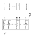
- FIG. 2 shows an exemplary schematic view of a QPP interleaver, consistent with certain disclosed embodiments.
- FIG. 3 shows an exemplary address generation apparatus for QPP interleaver, consistent with certain disclosed embodiments.
- FIG. 4 shows an exemplary schematic view of a corresponding group of increasing interleaver addresses or decreasing interleaver addresses generated by each QPP unit of the QPP interleaver address generation apparatus, consistent with certain disclosed embodiments.
- FIGS. 5A-5B show exemplary schematic views of hardware structure and control signal timing respectively of QPP unit 1 of FIG. 4 , consistent with certain disclosed embodiments.
- FIG. 6 shows an exemplary schematic view of hardware structure of QPP unit j of FIG. 4 , j ⁇ 2, consistent with certain disclosed embodiments.
- FIG. 7B shows an exemplary schematic view of the control signal timing sequence of the QPP unit 1 of FIG. 7A , consistent with certain disclosed embodiments.
- FIG. 9 shows an exemplary schematic view illustrating how QPP interleaver address generation apparatus may enable a plurality of MAP processors to output in parallel a plurality of data to memory, consistent with certain disclosed embodiments.
- FIG. 10 shows a working example illustrating how QPP interleaver address generation apparatus may enable the 40 data outputted in parallel by five MAP processors to be stored to memory, consistent with certain disclosed embodiments.
- FIG. 11 shows the usage of the bits of the interleaver address computed by each QPP unit in QPP interleaver address generation apparatus, consistent with certain disclosed embodiments.
- FIG. 13 shows an exemplary schematic view illustrating how QPP interleaver address generation apparatus generates corresponding increasing or decreasing interleaver addresses to correspond to the increasing or decreasing metric computation of MAP processor, consistent with certain disclosed embodiments.
- FIG. 14 shows an exemplary flowchart of an address generation method for QPP interleaver, consistent with certain disclosed embodiments.
- the exemplary embodiments of the present disclosure provide an address generation apparatus and method for QPP interleaver.
- the QPP address generation technology uses the design of a plurality of parallel computation circuits to compute the increasing or decreasing interleaver addresses, and is able to output the computation results in parallel.
- the QPP interleaver address generation apparatus may also be used as interleaver or de-interleaver address generator. When used as de-interleaver address generator, the output interleaver address is treated as reading a memory address.
- a QPP interleaver 200 utilizes a plurality of parallel computation circuits, such as, parallel computation circuits 1 to parallel computation circuit L, to output the address computation results in parallel, consistent with certain disclosed embodiments.
- the above design is attractive because targeting at different radix of MAP processor, the corresponding QPP interleaver addresses that QPP interleaver 200 directly computes in parallel and generates, may include increasing interleaver address or decreasing interleaver address to correspond to the increasing or decreasing metrics computation of the MAP processor.
- FIG. 3 shows an exemplary address generation apparatus for QPP interleaver, consistent with certain disclosed embodiments.
- QPP interleaver address generation apparatus 300 comprises L QPP units, represented as QPP unit 1 to QPP unit L, L ⁇ 2.
- a group of interleaver addresses outputted in parallel by each QPP unit j may be a group of increasing interleaver addresses 31 j or a group of decreasing interleaver addresses 32 j .
- the group of increasing interleaver addresses 31 j or decreasing interleaver addresses 32 j may be applied to a parallel decoder architecture of MAP processor of different radix architecture to correspond to the increasing or decreasing metrics computation of MAP processor.
- QPP unit j receives the computation result from the previous QPP unit j ⁇ 1 respectively, and simultaneously computes in parallel a corresponding group of increasing interleaver addresses 31 j or decreasing interleaver addresses 32 j .
- the group of increasing interleaver addresses 31 j and the group of decreasing interleaver addresses 32 j may be expressed as following, respectively: ⁇ ( i +( j ⁇ 1) M ), ⁇ ( i+ ( j ⁇ 1) M+ 1), . . . , ⁇ ( i+ ( j ⁇ 1) M+ ( r ⁇ 1)), and ⁇ ( jM ⁇ i ⁇ 1), ⁇ ( jM ⁇ i ⁇ 2), . . . ; ⁇ ( jM ⁇ i ⁇ r ), where M is the width of the sliding window of the outputted information of the inputted sequence.
- QPP unit 1 may compute in parallel the increasing interleaver addresses ⁇ (i), ⁇ (i+1), . . .
- QPP unit j may compute in parallel the increasing interleaver addresses ⁇ (i+(j ⁇ 1)M), ⁇ (i+(j ⁇ 1)M+1), . . . , ⁇ (i+(j ⁇ 1), M+(r ⁇ 1)); similarly, for 2 ⁇ j ⁇ L, QPP unit j may compute in parallel the decreasing interleaver addresses ⁇ (jM ⁇ i ⁇ 1), ⁇ (jM ⁇ i ⁇ 2), . . . , ⁇ (jM ⁇ i ⁇ r).
- M may be the memory length for the MAP processor to write to or read from.
- the original interleaving length k may be configured to the k/M interleaving lengths of M without the need to change the original decoder or processor circuit or structure.
- FIG. 4 shows an exemplary schematic view of a corresponding group of increasing interleaver addresses or decreasing interleaver addresses generated by each QPP unit of the QPP interleaver address generation apparatus, consistent with certain disclosed embodiments.
- QPP interleaver address generation apparatus 300 may input several configurable parameters, marked as 410 , such as parameters of k, (f 1 +f 2 ) mod k or f 2 ⁇ f 1 ⁇ 2(M ⁇ 1)f 2 mod k, 2f 2 mod k, f 1 M mod k, ⁇ (0) or ⁇ (M ⁇ 1), and uses the L QPP units to compute and output in parallel the interleaver addresses.
- Each QPP unit, 1 ⁇ j ⁇ L may follow the aforementioned equations to output in parallel a corresponding group (r) increasing interleaver addresses or a corresponding group (r) of decreasing interleaver addresses.
- FIG. 5A and FIG. 5B show respectively the exemplary schematic views of the hardware structure and control signal timing of QPP unit 1 of FIG. 4 , consistent with certain disclosed embodiments.
- the radix used by MAP processor is equal to 2 r
- r+1 multiplexers 510 - 51 r r registers 521 - 52 r and 2r 2-input-add-mod circuits, marked as 531 - 53 r and 541 - 54 r , may be used in combination with a control signal init 1 to realize QPP unit 1 .
- 2-input-add-mod circuit is a common remainder circuit, such as, two addition operands A and B, after addition, the remainder of divider K, i.e., (A+B) mod K, and may be realized by two adders and a multiplexer.
- FIG. 5B shows the control signal init 1 timing sequence. The following description refers to FIG. 5A and FIG. 5B to explain the operation among the components of QPP unit 1 .
- multiplexer 511 also outputs increasing parameter f 2 +f 1 +2f 2 ⁇ 2 or decreasing parameter f 2 ⁇ f 1 ⁇ 2(M ⁇ 3)f 2 to 2-input-add-mod circuit 541 ;
- multiplexer 512 outputs increasing parameter 0 or decreasing parameter ⁇ 2(M ⁇ 1)f 2 to 2-input-add-mod circuit 542 ;
- multiplexer 51 r outputs increasing parameter (2r ⁇ 4)f 2 or decreasing parameter ⁇ 2(M ⁇ r+1)f 2 to 2-input-add-mod circuit 54 r .
- the parameter is also outputted to 2-input-add-mod circuit 532 .
- the other input to 2-input-add-mod circuit 511 is increasing parameter 2(r ⁇ 1)f 2 or decreasing parameter ⁇ 2(M ⁇ r)f 2 .
- the generated modulus result R 1 is outputted to multiplexer 511 and 2-input-add-mod 531 and 542 - 54 r , respectively.
- the generated modulus result is outputted to multiplexer 513 and 2-input-add-mod 532 , respectively.
- the generated modulus result is outputted to register 522 and 2-input-add-mod 533 (not shown), respectively.
- 2-input-add-mod circuit 54 r computes, the generated modulus result is outputted to register 52 r.
- the r increasing interleaver addresses ⁇ (0) ⁇ (r ⁇ 1), or the r decreasing interleaver addresses ⁇ (M ⁇ 1) ⁇ (M ⁇ r) computed in parallel by the embodiment 500 of QPP unit 1 are stored into r registers 521 - 52 r respectively.
- the value stored in register 52 r i.e., ⁇ (r ⁇ 1) or ⁇ (M ⁇ r)
- the value is also outputted to 2-input-add-mod circuit 531 .
- QPP unit 1 in the embodiment 500 outputs the r interleaver addresses in registers 521 - 52 r , i.e., ⁇ (0)- ⁇ (r ⁇ 1) or ⁇ (M ⁇ 1) ⁇ (M ⁇ r). Because control signal init 1 is LOW, multiplexer 510 outputs the computation result of 2-input-add-mod circuit 531 , i.e., ⁇ (r) or ⁇ (M ⁇ r ⁇ 1), to register 521 . The computation result is also outputted to 2-input-add-mod circuit 532 .
- the generated modulus result of 2-input-add-mod circuit 511 is the modulus result of the previous modulus result R 1 and increasing parameter 2(r ⁇ 1)f 2 or decreasing parameter ⁇ 2(M ⁇ r)f 2 , and the new R 1 result is outputted to multiplexer 511 and 2-input-add-mod 531 and 542 - 54 r , respectively.
- Multiplexer 512 outputs parameter 2f 2 to 2-input-add-mod circuit 542 .
- the generated modulus result is outputted to multiplexer 513 and 2-input-add-mod 532 , respectively.
- the generated modulus result i.e., ⁇ (r+1) ⁇ (M ⁇ r ⁇ 2) is outputted to register 522 and 2-input-add-mod 533 , respectively.
- Multiplexer 51 r outputs parameter (2r ⁇ 2)f 2 to 2-input-add-mod circuit 54 r .
- the generated modulus result is outputted to 2-input-add-mod circuit 53 r .
- the generated modulus result i.e., ⁇ (2r ⁇ 1) ⁇ (M ⁇ 2r) is outputted to register 52 r .
- QPP unit 1 of embodiment 500 outputs the r interleaver addresses, i.e., ⁇ (r) ⁇ (2r ⁇ 1) or ⁇ (M ⁇ r ⁇ 1) ⁇ (M ⁇ 2r), stored in r registers 521 - 52 r .
- the value stored in register 52 r i.e., ⁇ (2r ⁇ 1) or ⁇ (M ⁇ 2r)
- the value is also outputted to 2-input-add-mod circuit 531 .
- QPP unit 1 of embodiment 500 may output in parallel the increasing interleaver addresses ⁇ (0)- ⁇ (r ⁇ 1) or decreasing interleaver addresses ⁇ (M ⁇ 1) ⁇ (M ⁇ r) first time; and for second time, QPP unit 1 of embodiment 500 may output in parallel the increasing interleaver addresses ⁇ (r) ⁇ (2r ⁇ 1) or decreasing interleaver addresses ⁇ (M ⁇ r ⁇ 1) ⁇ (M ⁇ 2r); and so on.
- the modulus operation by K must be performed on all negative numbers to transform the original values into positive numbers between 0 and K ⁇ 1, i.e., all the input signals must be positive numbers.
- FIG. 6 shows an exemplary schematic view of hardware structure of QPP unit j of FIG. 4 , j ⁇ 2, consistent with certain disclosed embodiments.
- the hardware structure of QPP unit j may be realized by r registers 621 - 62 r and r 2-input-add-mod circuits 631 - 63 r , with input parameter f 1 M.
- QPP unit j receives the computation result of previous QPP unit j ⁇ 1, and computes and outputs in parallel r increasing interleaver addresses ⁇ (x+(j ⁇ 1)M), ⁇ (x+(j ⁇ 1)M+1), . . .
- these increasing or decreasing interleaver addresses will also be outputted to the next QPP unit j+1.
- the hardware structure of QPP unit 1 may be designed according to the input increasing or decreasing parameter, in combination with different control signals, and outputs in parallel the corresponding group of increasing interleaver addresses 311 or decreasing interleaver addresses 321 , as described by the following two working examples.
- QPP unit 1 of working example 700 in FIG. 7A may be realized with six multiplexers 711 - 716 , three registers 721 - 723 , and six 2-input-add-mod circuits 701 - 706 , in combination with a control signal init 1 .
- multiplexer 711 outputs increasing parameter ⁇ (0) or decreasing parameter ⁇ (M ⁇ 1) to register 721 ; at this point, multiplexer 712 also outputs increasing parameter f 2 +f 1 +2f 2 ⁇ 2 or decreasing parameter f 2 ⁇ f 1 ⁇ 2(M ⁇ 3)f 2 to 2-input-add-mod circuit 702 ; multiplexer 713 also outputs increasing parameter f 2 +f 1 or decreasing parameter f 2 ⁇ f 1 ⁇ 2(M ⁇ 1)f 2 to 2-input-add-mod circuit 703 ; multiplexer 714 also outputs increasing parameter f 2 +f 1 +2f 2 or decreasing parameter f 2 ⁇ f 1 ⁇ 2(M ⁇ 2)f 2 to 2-input-add-mod circuit 704 .
- the parameter i.e., increasing parameter ⁇ (0) or decreasing parameter ⁇ (M ⁇ 1), is also output
- the other inputs to 2-input-add-mod circuits 702 - 704 are all parameter 2f 2 ⁇ 3.
- the generated modulus result R 1 is outputted to multiplexer 712 and 2-input-add-mod 701 , respectively.
- the generated modulus result R 2 is outputted to multiplexer 713 and multiplexer 715 , respectively.
- the generated modulus result R 2 is outputted to multiplexer 713 and multiplexer 715 , respectively.
- the generated modulus result R 3 is outputted to multiplexer 714 and multiplexer 716 , respectively.
- the generated modulus result i.e., ⁇ (1) or ⁇ (M ⁇ 2)
- the generated modulus result i.e., ⁇ (2) or ⁇ (M ⁇ 3)
- the generated modulus result i.e., ⁇ (2) or ⁇ (M ⁇ 3)
- the three increasing interleaver addresses ⁇ (0) ⁇ (2), or the three decreasing interleaver addresses ⁇ (M ⁇ 1) ⁇ (M ⁇ 3) computed in parallel by the QPP unit 1 of working example 700 are stored into three registers 721 - 723 , respectively.
- multiplexer 711 outputs the modulus result generated by 2-input-add-mod circuit 701 to register 721 , where one input of 2-input-add-mod circuit 701 is increasing parameter ⁇ (2) or decreasing parameter ⁇ (M ⁇ 3), and the other input of 2-input-add-mod circuit 701 is the modulus result generated by 2-input-add-mod circuit 702 .
- the modulus result generated by 2-input-add-mod circuit 702 is the modulus result of the previous modulus result R 1 and input parameter 2f 2 ⁇ 3.
- the generated modulus result i.e., increasing parameter ⁇ (3) or decreasing parameter ⁇ (M ⁇ 4), is outputted to 2-input-add-mod circuit 705 as well as register 721 .
- the modulus result generated by 2-input-add-mod circuit 703 is the modulus result of the previous modulus result R 2 and input parameter 2f 2 ⁇ 3, and is outputted by multiplexer 715 to 2-input-add-mod circuit 705 ;
- the modulus result generated by 2-input-add-mod circuit 704 is the modulus result of the previous modulus result R 3 and input parameter 2f 2 ⁇ 3, and is outputted by multiplexer 716 to 2-input-add-mod circuit 706 .
- the generated modulus result i.e., ⁇ (4) or decreasing parameter ⁇ (M ⁇ 5)
- the generated modulus result i.e., ⁇ (5) or decreasing parameter ⁇ (M ⁇ 6)
- the generated modulus result is outputted to register 723 and 2-input-add-mod circuit 701 , respectively.
- registers 721 - 723 store either increasing interleaver addresses ⁇ (0), ⁇ (1), ⁇ (2) or decreasing interleaver addresses ⁇ (M ⁇ 1), ⁇ (M ⁇ 2), ⁇ (M ⁇ 3); and for the second time, registers 721 - 723 store either increasing interleaver addresses ⁇ (3), ⁇ (4), ⁇ (5) or decreasing interleaver addresses ⁇ (M ⁇ 4), ⁇ (M ⁇ 5), ⁇ (M ⁇ 6); and so on.
- QPP unit 1 of working example 700 may output in parallel the increasing interleaver addresses ⁇ (0), ⁇ (1), ⁇ (2) or decreasing interleaver addresses ⁇ (M ⁇ 1), ⁇ (M ⁇ 2), ⁇ (M ⁇ 3) for the first time; and for second time, QPP unit 1 of working example 700 may output in parallel the increasing interleaver addresses ⁇ (3), ⁇ (4), ⁇ (5) or decreasing interleaver addresses ⁇ (M ⁇ 4), ⁇ (M ⁇ 5), ⁇ (M ⁇ 6); and so on.
- QPP unit 1 of working example 800 may be realized with six multiplexers 811 - 816 , two registers 821 - 822 , and three 2-input-add-mod circuits 801 - 803 , a 2-input-sub-mod circuit 804 , in combination with two control signals init 1 , init 2 .
- Registers 821 - 822 are controlled by the timing sequence of control signals init 1 , init 2 .
- registers 821 - 822 After the triggering edge of control signal mitt becomes LOW and triggers control signal init 2 , for the first time, registers 821 - 822 store either increasing interleaver addresses ⁇ (0), ⁇ (1) or decreasing interleaver addresses ⁇ (M ⁇ 1), ⁇ (M ⁇ 2)); and for the second time, registers 821 - 822 store either increasing interleaver addresses ⁇ (2), ⁇ (3) or decreasing interleaver addresses ⁇ (M ⁇ 3), ⁇ (M ⁇ 4); and so on.
- QPP unit 1 of working example 800 is different in the increasing parameter and the decreasing parameter input, in combination with the two control signals, and 2-input-add-mod circuits and 2-input-sub-mod circuits to realize the hardware structure of QPP unit 1 , wherein control signal init 1 is triggered first to set the output of multiplexers 811 - 815 ; when the triggering edge of control signal init 1 becomes LOW, multiplexers 816 is set by triggering control signal init 2 to output the modulus result generated by 2-input-sub-mod circuit 804 to multiplexer 815 .
- the hardware structure design of QPP unit 1 in FIG. 5A is the most compact design for MAP processors using the same radix ( 2 r ), where the hardware structure design of FIG. 5A uses less multiplexers and only one control signal.
- FIG. 9 shows an exemplary schematic view illustrating how QPP interleaver address generation apparatus may allow a plurality of MAP processors to output in parallel a plurality of data to memory, consistent with certain disclosed embodiments.
- QPP interleaver address generation apparatus 300 generates interleaver addresses ⁇ (i), ⁇ (i+M), ⁇ (i+2M), . . . , ⁇ (i+(L ⁇ 1)M), and outputs memory selection information 920 to a data multiplexer 910 .
- Memory selection information is information on partial bits of ⁇ (i), ⁇ (i+M), ⁇ (i+2M), . . . , ⁇ (i+(L ⁇ 1)M), such as, information on the n most significant bits (MSB) of ⁇ (i), ⁇ (i+M), ⁇ (i+2M), . . . , ⁇ (i+(L ⁇ 1)M).
- LSB least significant bits
- FIG. 10 shows an exemplary schematic view of how QPP interleaver address generation apparatus 300 enables five MAP processors, such as, MAP processor 1 - MAP processor 5 , to store 40 data into the memory addresses generated by QPP interleaver address generation apparatus 300 .
- QPP interleaver address generation apparatus 300 computes in parallel interleaver addresses ⁇ (i), ⁇ (i+8), ⁇ (i+16), ⁇ (i+24), ⁇ (i+32)
- QPP interleaver address generation apparatus 300 also outputs information 1020 on the MSB 3 bits of ⁇ (i), ⁇ (i+8), ⁇ (i+16), ⁇ (i+24), ⁇ (i+32) to data multiplexer 1010 at the same time.
- the five memories are determined by information 1020 on the MSB 3 bits of ⁇ (i), ⁇ (i+8), ⁇ (i+16), ⁇ (i+24), ⁇ (i+32), and the memory addresses to be written into are determined by information 1050 on the LSB 3 bits of ⁇ (i), ⁇ (i+8), ⁇ (i+16), ⁇ (i+24), ⁇ (i+32).
- the five data are outputted in parallel to five different memories and the five memories use the same memory address to store the data respectively.
- MAP processor 1 - MAP processor 5 output 40 data in parallel totally, and the data are stored into the memory addresses of the five different memories.
- n may be seen as the number of bits of the address buses of the memory. In other words, each memory has 2 n memory addresses.
- the MSB n bits of the interleaver addresses computed by L QPP units i.e., ⁇ (i), ⁇ (i+M), . . . , ⁇ (i+(L ⁇ 1)M), may be mapped to L MAP processors to select the memory for the processed data to write into.
- FIG. 12 shows an exemplary table of how QPP interleaver address generation apparatus computes interleaver addresses and determines memory addresses, consistent with certain disclosed embodiments.
- the MSB 3 bits of ⁇ (0), ⁇ (8), ⁇ (16), ⁇ (24), ⁇ (32) are 000, 011, 001, 100, 010, respectively, and the LSB 3 bits of ⁇ (0) is 000, therefore, for the first time, the five data (i.e., data 0 , data 8 , data 16 , data 24 , data 32 ) outputted in parallel by five MAP processors (MAP processor 1 - MAP processor 5 ) are written to the address 0 of memory 0 , address 0 of memory 3 , address 0 of memory 1 , address 0 of memory 4 and address 0 of memory 2 , respectively.
- the MSB 3 bits of ⁇ (1), ⁇ (9), ⁇ (17), ⁇ (25), ⁇ (33) are 001, 100, 010, 000, 011, respectively, and the LSB 3 bits of ⁇ (1) is 101, therefore, for the second time, the five data (i.e., data 1 , data 9 , data 17 , data 25 , data 33 ) outputted in parallel by five MAP processors (MAP processor 1 to MAP processor 5 ) are written to the address 5 of memory 1 , address 5 of memory 4 , address 5 of memory 2 , address 5 of memory 0 and address 5 of memory 3 , respectively; and so on.
- each memory includes 8 addresses, i.e., address 0 to address 7 , so that 8 data outputted by each of Map processors may be written into the 8 addresses of a corresponding memory.
- the computation does not need complicated circuit, such as, multiplier, and the five data outputted in parallel by MAP processor 1 to MAP processor 5 are written to the same address of memory 0 to memory 4 .
- the LSB n bits of the interleaver addresses computed by QPP unit 1 may be used as the memory address to write into.
- QPP interleaver address generation apparatus 300 may generate corresponding increasing or decreasing interleaver addresses to correspond to the increasing or decreasing metric computation of the MAP processor, as shown in the example of FIG. 13 .
- a MAP of soft-input and soft-output (SISO) unit 1310 reads the increasing input signal or decreasing input signal L e (Z k,1 ), I a (x k ) and L e (x k )
- QPP interleaver address generation apparatus 300 will generate increasing interleaver addresses or decreasing interleaver addresses ⁇ (i) for different memories to read corresponding L e (Z k,1 ), I a (x k ) and L e (x k ) used as input signal of the MAP.
- QPP interleaver address generation apparatus 300 may also generate corresponding interleaver address to provide the MAP to write computation result into a memory 1320 , where
- FIG. 14 shows an exemplary flowchart of an address generation method for QPP interleaver, consistent with certain disclosed embodiments.
- step 1420 it computes and outputs a plurality of interleaver addresses by using L QPP units, wherein each QPP unit j, 1 ⁇ j ⁇ L, is a parallel computation unit and outputs in parallel a corresponding group of interleaver addresses, where ⁇ (i) is an i th interleaving address generated by the method, f 1 and f 2 are QPP coefficients, k is information block length of an input sequence. So that, the input sequence of information is stored into the plurality of corresponding memory addresses, 0 ⁇ i ⁇ k ⁇ 1, 1 ⁇ j ⁇ L. The input sequence of information may be outputted in parallel through L sliding windows, and M is the width of each of the L sliding windows.
- the group of interleaver addresses outputted by each QPP unit j in parallel may be either a group of increasing interleaver addresses or a group of decreasing interleaver addresses.
- each QPP unit j may compute a corresponding group of increasing interleaver addresses or a group of decreasing interleaver addresses in parallel according to the aforementioned equations (1)-(5), and the description is omitted here.
- the LSB n bits of interleaver address ⁇ (i) computed by QPP unit 1 may be used as the memory address, and the MSB n bits of interleaver address ⁇ (i+(j ⁇ 1)M) computed by each QPP unit j, 1 ⁇ j ⁇ L, may be provided to a data multiplexer to select a memory from a plurality of memories.
- Each data of the input sequence may be written to a corresponding memory address based on the memory selected through the MSB n bits and the address designated by LSB n bits.
- the disclosed exemplary embodiments provide an address generation apparatus and method for QPP interleaver.
- a plurality of QPP units may directly compute increasing interleaver addresses or decreasing interleaver address.
- Each QPP unit may compute and output a corresponding group of interleaver addresses or decreasing interleaver addresses in parallel.
- each original parallel output of interleaver address may be expanded to r parallel interleaver addresses for output.
- the corresponding increasing interleaver address or decreasing address may be generated to correspond to the increasing or decreasing metric computation of the MAP processor.
- the QPP interleaver address generation apparatus of the disclosed exemplary embodiments may configure the original interleaver length K into KIM interleaver lengths of M without changing the original circuit.
- the disclosed exemplary embodiments use low complexity circuits, and need no memory space to store interleaver addresses, so that the hardware area is greatly reduced and the computation speed for interleaver address is improved.
- the disclosed exemplary embodiments may be applicable to mobile communication systems, such as, 3GPPLTE and LTE-A.
Landscapes
- Physics & Mathematics (AREA)
- Probability & Statistics with Applications (AREA)
- Engineering & Computer Science (AREA)
- Theoretical Computer Science (AREA)
- Mathematical Physics (AREA)
- Error Detection And Correction (AREA)
Abstract
Description
Π(n)=(f 1 n+f 2 n 2)mod k, n=0, 1, . . . , k−1,
where Π(n) is the n-th interleaved output position, f1 and f2 are QPP coefficients, k is the information block length of the input sequence and mod is the modulus operation.
Π(i+(j−1)M), Π(i+(j−1)M+1), . . . , Π(i+(j−1)M+(r−1)), and
Π(jM−i−1), Π(jM−i−2), . . . ; Π(jM−i−r),
where M is the width of the sliding window of the outputted information of the inputted sequence.
Π(i+1)=(f 1(i+1)+f 2(i+1)2)mod k=(Π(i)+f 2 +f 1+2f 2 i)mod k, i=0, 1, . . . , k−1 (1),
and a group of decreasing interleaver addresses 321 corresponding to
Π(i−1)=(f 1(i−1)+f 2(i−1)2)mod k=(Π(i)+f 2 −f 1−2f 2 i)mod k, i=0, 1, . . . , k−1 (2)
In this manner,
Π(i+(j−1)M)=(Π(i+(j−2)M)+f 1 M+(2j−3)f 2 M 2+2f 2 Mi)mod k (3),
Π(i+(j−1)M+1)=(Π(i+(j−2)M+1)+f 1 M+(2j−3)f 2 M 2+2f 2 M(i+1))mod k (4),
Π(i+(j−1)M+(r−1))=(Π(i+(j−2)M+(r−1)+f 1 M+(2j−3)f 2 M 2+2f 2 M(i+(r−1))mod k (5)
Π(0)=0=(000000)2,Π(8)=24=(011000)2,
Π(16)=8=(001000)2,Π(24)=32=(100000)2,
Π(32)=16=(010000)2.
Π(1)=13=(001101)2,Π(9)=37=(100101)2,
Π(17)=21=(010101)2,Π(25)=5=(000101)2,
Π(33)=29=(011101)2.
Claims (16)
Applications Claiming Priority (3)
| Application Number | Priority Date | Filing Date | Title |
|---|---|---|---|
| TW99127734A | 2010-08-19 | ||
| TW099127734 | 2010-08-19 | ||
| TW099127734A TW201209711A (en) | 2010-08-19 | 2010-08-19 | Address generation apparatus and method for quadratic permutation polynomial interleaver |
Publications (2)
| Publication Number | Publication Date |
|---|---|
| US20120047414A1 US20120047414A1 (en) | 2012-02-23 |
| US8468410B2 true US8468410B2 (en) | 2013-06-18 |
Family
ID=45595026
Family Applications (1)
| Application Number | Title | Priority Date | Filing Date |
|---|---|---|---|
| US12/892,199 Active 2031-09-22 US8468410B2 (en) | 2010-08-19 | 2010-09-28 | Address generation apparatus and method for quadratic permutation polynomial interleaver |
Country Status (2)
| Country | Link |
|---|---|
| US (1) | US8468410B2 (en) |
| TW (1) | TW201209711A (en) |
Cited By (2)
| Publication number | Priority date | Publication date | Assignee | Title |
|---|---|---|---|---|
| CN104077414A (en) * | 2014-07-16 | 2014-10-01 | 武汉虹信通信技术有限责任公司 | Decoding device and decoding method applied to LTE network signals |
| CN109061296A (en) * | 2018-07-17 | 2018-12-21 | 南京恒电电子有限公司 | A kind of high-precision carrier frequency estimation method of RF pulse signal |
Families Citing this family (2)
| Publication number | Priority date | Publication date | Assignee | Title |
|---|---|---|---|---|
| US8429510B2 (en) * | 2010-10-26 | 2013-04-23 | Lsi Corporation | Simplified parallel address-generation for interleaver |
| CN112751572B (en) * | 2021-01-07 | 2023-03-14 | 西安电子科技大学 | Four-path parallel LTE-based 4Turbo interleaving address generation method |
Citations (8)
| Publication number | Priority date | Publication date | Assignee | Title |
|---|---|---|---|---|
| US20020159423A1 (en) | 2001-02-28 | 2002-10-31 | Iwen Yao | Interleaver for turbo decoder |
| US20080115034A1 (en) * | 2006-11-10 | 2008-05-15 | Telefonaktiebolaget Lm Ericsson (Publ) | QPP Interleaver/De-Interleaver for Turbo Codes |
| US20080172590A1 (en) | 2007-01-17 | 2008-07-17 | Broadcom Corporation, A California Corporation | Quadratic polynomial permutation (QPP) interleaver providing hardware savings and flexible granularity adaptable to any possible turbo code block size |
| US20080172591A1 (en) | 2007-01-17 | 2008-07-17 | Broadcom Corporation, A California Corporation | Formulaic flexible collision-free memory accessing for parallel turbo decoding with quadratic polynomial permutation (QPP) interleave |
| US20090249024A1 (en) * | 2008-03-31 | 2009-10-01 | Jones Ben J | Address generation for quadratic permutation polynomial interleaving |
| US20100005221A1 (en) * | 2008-07-03 | 2010-01-07 | Nokia Corporation | Address generation for multiple access of memory |
| US20100070737A1 (en) * | 2008-09-18 | 2010-03-18 | Xilinx, Inc. | Address generation |
| CN101777923A (en) | 2009-01-09 | 2010-07-14 | 华为技术有限公司 | CTC (Convolutional Turbo Code) encoder, internal code interleaver, as well as internal code interleaving method and encoding processing method |
-
2010
- 2010-08-19 TW TW099127734A patent/TW201209711A/en unknown
- 2010-09-28 US US12/892,199 patent/US8468410B2/en active Active
Patent Citations (8)
| Publication number | Priority date | Publication date | Assignee | Title |
|---|---|---|---|---|
| US20020159423A1 (en) | 2001-02-28 | 2002-10-31 | Iwen Yao | Interleaver for turbo decoder |
| US20080115034A1 (en) * | 2006-11-10 | 2008-05-15 | Telefonaktiebolaget Lm Ericsson (Publ) | QPP Interleaver/De-Interleaver for Turbo Codes |
| US20080172590A1 (en) | 2007-01-17 | 2008-07-17 | Broadcom Corporation, A California Corporation | Quadratic polynomial permutation (QPP) interleaver providing hardware savings and flexible granularity adaptable to any possible turbo code block size |
| US20080172591A1 (en) | 2007-01-17 | 2008-07-17 | Broadcom Corporation, A California Corporation | Formulaic flexible collision-free memory accessing for parallel turbo decoding with quadratic polynomial permutation (QPP) interleave |
| US20090249024A1 (en) * | 2008-03-31 | 2009-10-01 | Jones Ben J | Address generation for quadratic permutation polynomial interleaving |
| US20100005221A1 (en) * | 2008-07-03 | 2010-01-07 | Nokia Corporation | Address generation for multiple access of memory |
| US20100070737A1 (en) * | 2008-09-18 | 2010-03-18 | Xilinx, Inc. | Address generation |
| CN101777923A (en) | 2009-01-09 | 2010-07-14 | 华为技术有限公司 | CTC (Convolutional Turbo Code) encoder, internal code interleaver, as well as internal code interleaving method and encoding processing method |
Non-Patent Citations (8)
| Title |
|---|
| A. Nimbalker, Daniel J. Costello, "Contention-Free Interleavers for High-Throughput Turbo decoding", IEEE Trans. on Communications, Aug. 8, 2008, p. 1258-p. 1267. |
| A. Nimbalker, Y. Blankenship, B. Classon, T. Keith Blankenship, "ARP and QPP interleavers forLTE Turbo coding", IEEE WCNC , Mar. 31, 2008, p. 1032-p. 1037. |
| J. Sun and O. Y. Takeshita, "Interleavers for turbo codes using permutation polynomials over integer rings," IEEE Trans. on Inform. Theory, vol. 51, No. 1, pp. 101-119, Jan. 2005. |
| L. Zhang, Y. Xu, X. Ma, H. Luo, and X. Gan, "Study on Interleaver Design for Turbo codes using Permutation Polynomials over integer rings", IEEE VTC, Sep. 25, 2006, p. 1-p. 5. |
| Maurizio Martina, Mario Nicola, and Guido Masera, "A Flexible UMTS-WiMax Turbo Decoder Architecture", IEEE Transactions on Circuits and Systems-II: Express Briefs, vol. 55, No. 4, Apr. 2008. |
| Oscar Y. Takeshita et al., "New Deterministic Interleaver Designs for Turbo Codes", IEEE Tran. on Information Theory, Sep. 6, 2000, p. 1988-p. 2006. |
| R. Dobkin, M. Peleg, and R. Ginosar, "Parallel interleaver design and VLSI architecture for low-latency MAP turbo decoders," IEEE Trans. on VLSI Systems, vol. 13, No. 4, pp. 427-438, Apr. 2005. |
| U.S. Appl. No. 12/647,394, filed Dec. 25, 2009. |
Cited By (4)
| Publication number | Priority date | Publication date | Assignee | Title |
|---|---|---|---|---|
| CN104077414A (en) * | 2014-07-16 | 2014-10-01 | 武汉虹信通信技术有限责任公司 | Decoding device and decoding method applied to LTE network signals |
| CN104077414B (en) * | 2014-07-16 | 2017-07-25 | 武汉虹信通信技术有限责任公司 | A kind of decoding apparatus and its coding/decoding method applied to LTE network signal |
| CN109061296A (en) * | 2018-07-17 | 2018-12-21 | 南京恒电电子有限公司 | A kind of high-precision carrier frequency estimation method of RF pulse signal |
| CN109061296B (en) * | 2018-07-17 | 2020-11-27 | 南京恒电电子有限公司 | High-precision carrier frequency estimation method for radio frequency pulse signal |
Also Published As
| Publication number | Publication date |
|---|---|
| TW201209711A (en) | 2012-03-01 |
| US20120047414A1 (en) | 2012-02-23 |
Similar Documents
| Publication | Publication Date | Title |
|---|---|---|
| JP5499368B2 (en) | Data interleaving circuit and method for vectorized turbo decoder | |
| US8332701B2 (en) | Address generation apparatus and method for quadratic permutation polynomial interleaver de-interleaver | |
| Wang et al. | Parallel interleaver design for a high throughput HSPA+/LTE multi-standard turbo decoder | |
| US9048877B2 (en) | Turbo code parallel interleaver and parallel interleaving method thereof | |
| Sun et al. | Configurable and scalable high throughput turbo decoder architecture for multiple 4G wireless standards | |
| US8806290B2 (en) | Systems and methods for parallel dual-mode turbo decoders | |
| JP6022085B2 (en) | Method and apparatus for realizing multimode decoder | |
| JP2007068155A (en) | Method and system of interleaving in parallel turbo decoder | |
| CN104092470B (en) | A kind of Turbo code code translator and method | |
| US8468410B2 (en) | Address generation apparatus and method for quadratic permutation polynomial interleaver | |
| WO2012083714A1 (en) | Method for turbo codes data interleaving and interleaver for interleaving turbo codes data | |
| CN101707490A (en) | Parallel Turbo code interleaving method | |
| Prescher et al. | A parametrizable low-power high-throughput turbo-decoder | |
| US7278088B2 (en) | Configurable architecture and its implementation of viterbi decorder | |
| US20110087949A1 (en) | Reconfigurable turbo interleavers for multiple standards | |
| CN102130696A (en) | Interleaving/de-interleaving method, soft-in/soft-out decoding method and error correction code encoder and decoder utilizing the same | |
| EP1739843B1 (en) | Power efficient Viterbi decoder | |
| JP2009246474A (en) | Turbo decoder | |
| Yoo et al. | Reverse rate matching for low-power LTE-advanced turbo decoders | |
| CN110022158B (en) | Decoding method and device | |
| Murugappa et al. | Parameterized area-efficient multi-standard turbo decoder | |
| CN104184536B (en) | Sub-block intertexture control method, device and equipment based on LTE Turbo decodings | |
| US20140223267A1 (en) | Radix-4 viterbi forward error correction decoding | |
| US8627022B2 (en) | Contention free parallel access system and a method for contention free parallel access to a group of memory banks | |
| CN102025380B (en) | Quadratic permutation polynomial interleaver address generation device and method |
Legal Events
| Date | Code | Title | Description |
|---|---|---|---|
| AS | Assignment |
Owner name: NATIONAL CHIAO TUNG UNIVERSITY, TAIWAN Free format text: ASSIGNMENT OF ASSIGNORS INTEREST;ASSIGNORS:LEE, SHUENN-GI;WANG, CHUNG HSUAN;SHEEN, WERN-HO;REEL/FRAME:025053/0709 Effective date: 20100914 Owner name: INDUSTRIAL TECHNOLOGY RESEARCH INSTITUTE, TAIWAN Free format text: ASSIGNMENT OF ASSIGNORS INTEREST;ASSIGNORS:LEE, SHUENN-GI;WANG, CHUNG HSUAN;SHEEN, WERN-HO;REEL/FRAME:025053/0709 Effective date: 20100914 |
|
| STCF | Information on status: patent grant |
Free format text: PATENTED CASE |
|
| FPAY | Fee payment |
Year of fee payment: 4 |
|
| MAFP | Maintenance fee payment |
Free format text: PAYMENT OF MAINTENANCE FEE, 8TH YEAR, LARGE ENTITY (ORIGINAL EVENT CODE: M1552); ENTITY STATUS OF PATENT OWNER: LARGE ENTITY Year of fee payment: 8 |