US8456594B2 - Cholesteric liquid crystal display devices and methods of manufacturing the same - Google Patents
Cholesteric liquid crystal display devices and methods of manufacturing the same Download PDFInfo
- Publication number
- US8456594B2 US8456594B2 US12/659,558 US65955810A US8456594B2 US 8456594 B2 US8456594 B2 US 8456594B2 US 65955810 A US65955810 A US 65955810A US 8456594 B2 US8456594 B2 US 8456594B2
- Authority
- US
- United States
- Prior art keywords
- liquid crystal
- subpixel
- chiral dopant
- cholesteric
- subpixel unit
- Prior art date
- Legal status (The legal status is an assumption and is not a legal conclusion. Google has not performed a legal analysis and makes no representation as to the accuracy of the status listed.)
- Expired - Fee Related, expires
Links
Images


Classifications
-
- G—PHYSICS
- G02—OPTICS
- G02F—OPTICAL DEVICES OR ARRANGEMENTS FOR THE CONTROL OF LIGHT BY MODIFICATION OF THE OPTICAL PROPERTIES OF THE MEDIA OF THE ELEMENTS INVOLVED THEREIN; NON-LINEAR OPTICS; FREQUENCY-CHANGING OF LIGHT; OPTICAL LOGIC ELEMENTS; OPTICAL ANALOGUE/DIGITAL CONVERTERS
- G02F1/00—Devices or arrangements for the control of the intensity, colour, phase, polarisation or direction of light arriving from an independent light source, e.g. switching, gating or modulating; Non-linear optics
- G02F1/01—Devices or arrangements for the control of the intensity, colour, phase, polarisation or direction of light arriving from an independent light source, e.g. switching, gating or modulating; Non-linear optics for the control of the intensity, phase, polarisation or colour
- G02F1/13—Devices or arrangements for the control of the intensity, colour, phase, polarisation or direction of light arriving from an independent light source, e.g. switching, gating or modulating; Non-linear optics for the control of the intensity, phase, polarisation or colour based on liquid crystals, e.g. single liquid crystal display cells
- G02F1/137—Devices or arrangements for the control of the intensity, colour, phase, polarisation or direction of light arriving from an independent light source, e.g. switching, gating or modulating; Non-linear optics for the control of the intensity, phase, polarisation or colour based on liquid crystals, e.g. single liquid crystal display cells characterised by the electro-optical or magneto-optical effect, e.g. field-induced phase transition, orientation effect, guest-host interaction or dynamic scattering
-
- C—CHEMISTRY; METALLURGY
- C09—DYES; PAINTS; POLISHES; NATURAL RESINS; ADHESIVES; COMPOSITIONS NOT OTHERWISE PROVIDED FOR; APPLICATIONS OF MATERIALS NOT OTHERWISE PROVIDED FOR
- C09K—MATERIALS FOR MISCELLANEOUS APPLICATIONS, NOT PROVIDED FOR ELSEWHERE
- C09K19/00—Liquid crystal materials
- C09K19/52—Liquid crystal materials characterised by components which are not liquid crystals, e.g. additives with special physical aspect: solvents, solid particles
- C09K19/54—Additives having no specific mesophase characterised by their chemical composition
- C09K19/542—Macromolecular compounds
- C09K19/544—Macromolecular compounds as dispersing or encapsulating medium around the liquid crystal
-
- C—CHEMISTRY; METALLURGY
- C09—DYES; PAINTS; POLISHES; NATURAL RESINS; ADHESIVES; COMPOSITIONS NOT OTHERWISE PROVIDED FOR; APPLICATIONS OF MATERIALS NOT OTHERWISE PROVIDED FOR
- C09K—MATERIALS FOR MISCELLANEOUS APPLICATIONS, NOT PROVIDED FOR ELSEWHERE
- C09K19/00—Liquid crystal materials
- C09K19/52—Liquid crystal materials characterised by components which are not liquid crystals, e.g. additives with special physical aspect: solvents, solid particles
- C09K19/58—Dopants or charge transfer agents
- C09K19/586—Optically active dopants; chiral dopants
-
- G—PHYSICS
- G02—OPTICS
- G02F—OPTICAL DEVICES OR ARRANGEMENTS FOR THE CONTROL OF LIGHT BY MODIFICATION OF THE OPTICAL PROPERTIES OF THE MEDIA OF THE ELEMENTS INVOLVED THEREIN; NON-LINEAR OPTICS; FREQUENCY-CHANGING OF LIGHT; OPTICAL LOGIC ELEMENTS; OPTICAL ANALOGUE/DIGITAL CONVERTERS
- G02F1/00—Devices or arrangements for the control of the intensity, colour, phase, polarisation or direction of light arriving from an independent light source, e.g. switching, gating or modulating; Non-linear optics
- G02F1/01—Devices or arrangements for the control of the intensity, colour, phase, polarisation or direction of light arriving from an independent light source, e.g. switching, gating or modulating; Non-linear optics for the control of the intensity, phase, polarisation or colour
- G02F1/13—Devices or arrangements for the control of the intensity, colour, phase, polarisation or direction of light arriving from an independent light source, e.g. switching, gating or modulating; Non-linear optics for the control of the intensity, phase, polarisation or colour based on liquid crystals, e.g. single liquid crystal display cells
- G02F1/137—Devices or arrangements for the control of the intensity, colour, phase, polarisation or direction of light arriving from an independent light source, e.g. switching, gating or modulating; Non-linear optics for the control of the intensity, phase, polarisation or colour based on liquid crystals, e.g. single liquid crystal display cells characterised by the electro-optical or magneto-optical effect, e.g. field-induced phase transition, orientation effect, guest-host interaction or dynamic scattering
- G02F1/13718—Devices or arrangements for the control of the intensity, colour, phase, polarisation or direction of light arriving from an independent light source, e.g. switching, gating or modulating; Non-linear optics for the control of the intensity, phase, polarisation or colour based on liquid crystals, e.g. single liquid crystal display cells characterised by the electro-optical or magneto-optical effect, e.g. field-induced phase transition, orientation effect, guest-host interaction or dynamic scattering based on a change of the texture state of a cholesteric liquid crystal
-
- G—PHYSICS
- G02—OPTICS
- G02F—OPTICAL DEVICES OR ARRANGEMENTS FOR THE CONTROL OF LIGHT BY MODIFICATION OF THE OPTICAL PROPERTIES OF THE MEDIA OF THE ELEMENTS INVOLVED THEREIN; NON-LINEAR OPTICS; FREQUENCY-CHANGING OF LIGHT; OPTICAL LOGIC ELEMENTS; OPTICAL ANALOGUE/DIGITAL CONVERTERS
- G02F1/00—Devices or arrangements for the control of the intensity, colour, phase, polarisation or direction of light arriving from an independent light source, e.g. switching, gating or modulating; Non-linear optics
- G02F1/01—Devices or arrangements for the control of the intensity, colour, phase, polarisation or direction of light arriving from an independent light source, e.g. switching, gating or modulating; Non-linear optics for the control of the intensity, phase, polarisation or colour
- G02F1/17—Devices or arrangements for the control of the intensity, colour, phase, polarisation or direction of light arriving from an independent light source, e.g. switching, gating or modulating; Non-linear optics for the control of the intensity, phase, polarisation or colour based on variable-absorption elements not provided for in groups G02F1/015 - G02F1/169
-
- G—PHYSICS
- G02—OPTICS
- G02F—OPTICAL DEVICES OR ARRANGEMENTS FOR THE CONTROL OF LIGHT BY MODIFICATION OF THE OPTICAL PROPERTIES OF THE MEDIA OF THE ELEMENTS INVOLVED THEREIN; NON-LINEAR OPTICS; FREQUENCY-CHANGING OF LIGHT; OPTICAL LOGIC ELEMENTS; OPTICAL ANALOGUE/DIGITAL CONVERTERS
- G02F1/00—Devices or arrangements for the control of the intensity, colour, phase, polarisation or direction of light arriving from an independent light source, e.g. switching, gating or modulating; Non-linear optics
- G02F1/01—Devices or arrangements for the control of the intensity, colour, phase, polarisation or direction of light arriving from an independent light source, e.g. switching, gating or modulating; Non-linear optics for the control of the intensity, phase, polarisation or colour
- G02F1/13—Devices or arrangements for the control of the intensity, colour, phase, polarisation or direction of light arriving from an independent light source, e.g. switching, gating or modulating; Non-linear optics for the control of the intensity, phase, polarisation or colour based on liquid crystals, e.g. single liquid crystal display cells
- G02F1/133—Constructional arrangements; Operation of liquid crystal cells; Circuit arrangements
- G02F1/1333—Constructional arrangements; Manufacturing methods
- G02F1/133377—Cells with plural compartments or having plurality of liquid crystal microcells partitioned by walls, e.g. one microcell per pixel
-
- G—PHYSICS
- G02—OPTICS
- G02F—OPTICAL DEVICES OR ARRANGEMENTS FOR THE CONTROL OF LIGHT BY MODIFICATION OF THE OPTICAL PROPERTIES OF THE MEDIA OF THE ELEMENTS INVOLVED THEREIN; NON-LINEAR OPTICS; FREQUENCY-CHANGING OF LIGHT; OPTICAL LOGIC ELEMENTS; OPTICAL ANALOGUE/DIGITAL CONVERTERS
- G02F1/00—Devices or arrangements for the control of the intensity, colour, phase, polarisation or direction of light arriving from an independent light source, e.g. switching, gating or modulating; Non-linear optics
- G02F1/01—Devices or arrangements for the control of the intensity, colour, phase, polarisation or direction of light arriving from an independent light source, e.g. switching, gating or modulating; Non-linear optics for the control of the intensity, phase, polarisation or colour
- G02F1/13—Devices or arrangements for the control of the intensity, colour, phase, polarisation or direction of light arriving from an independent light source, e.g. switching, gating or modulating; Non-linear optics for the control of the intensity, phase, polarisation or colour based on liquid crystals, e.g. single liquid crystal display cells
- G02F1/137—Devices or arrangements for the control of the intensity, colour, phase, polarisation or direction of light arriving from an independent light source, e.g. switching, gating or modulating; Non-linear optics for the control of the intensity, phase, polarisation or colour based on liquid crystals, e.g. single liquid crystal display cells characterised by the electro-optical or magneto-optical effect, e.g. field-induced phase transition, orientation effect, guest-host interaction or dynamic scattering
- G02F1/13775—Polymer-stabilized liquid crystal layers
-
- G—PHYSICS
- G02—OPTICS
- G02F—OPTICAL DEVICES OR ARRANGEMENTS FOR THE CONTROL OF LIGHT BY MODIFICATION OF THE OPTICAL PROPERTIES OF THE MEDIA OF THE ELEMENTS INVOLVED THEREIN; NON-LINEAR OPTICS; FREQUENCY-CHANGING OF LIGHT; OPTICAL LOGIC ELEMENTS; OPTICAL ANALOGUE/DIGITAL CONVERTERS
- G02F2203/00—Function characteristic
- G02F2203/34—Colour display without the use of colour mosaic filters
Definitions
- Example embodiments relate to cholesteric liquid crystal display devices having a single-layered structure and methods of manufacturing the same.
- a cholesteric liquid crystal is a liquid crystal composition formed by twisting a nematic liquid crystal into a helix structure.
- a cholesteric liquid crystal has a light reflection property, which varies according to a helix pitch. More specifically, light having a given, desired or predetermined wavelength range is selectively reflected according to a helix pitch of a liquid crystal molecule. Thus, a full-color image is produced by controlling a reflection wavelength range by using pixels having different helix pitches.
- a cholesteric liquid crystal having these display characteristics has relatively clear color display characteristics, relatively high contrast characteristics, and relatively high resolution characteristics.
- a display device using cholesteric liquid crystals shows relatively high performance.
- a method of producing a full-color image using cholesteric liquid crystals is performed in a multilayer manner or a single layer manner.
- a red (R) pixel, a green (G) pixel, and a blue (B) pixel are stacked on each other.
- the red (R) pixel has a helix pitch that is controlled such that light having a red wavelength range is selectively reflected.
- the green (G) pixel has a helix pitch that is controlled such that light having a green wavelength range is selectively reflected.
- the blue (B) pixel has a helix pitch that is controlled such that light having a blue wavelength range is selectively reflected.
- the respective pixels are controlled to be in a wavelength selection reflection mode or transmission mode, according to the application of a voltage, and a color corresponding to a pixel being in the wavelength selection reflection mode is displayed.
- the multilayer manner is relatively complicated and expensive at least because a multi-layer substrate is used.
- the multilayer manner also provides relatively low color purity due to a scattering phenomenon that may occur in a pixel that is in the transmission mode.
- Example embodiments provide cholesteric liquid crystal display devices having improved color image quality and methods of manufacturing the same.
- the display device includes: a plurality of pixel units.
- Each of the pixel units includes a cholesteric liquid crystal layer.
- the cholesteric liquid crystal layer is interposed between two transparent substrates.
- the cholesteric liquid crystal layer includes: a liquid crystal molecule; a chiral dopant; and an optically polymerizable polymer.
- the chiral dopant is mixed with the liquid crystal molecule to form a cholesteric phase.
- the solubility of the chiral dopant with respect to the liquid crystal molecule varies according to temperature.
- the optically polymerizable polymer is cured to fix a helix pitch of the cholesteric phase.
- the pixel units are arranged two-dimensionally and the cholesteric liquid crystal layer of each of the pixel units has a single-layered structure.
- each of the pixel units may include a plurality of subpixel units.
- Each of the plurality of subpixel units may have different helix pitches of the cholesteric phase.
- each of the pixel units may include a red subpixel unit, a green subpixel unit, and a blue subpixel unit.
- each of the pixel units may include a magenta subpixel unit, a yellow subpixel unit, and a cyan subpixel unit.
- Barrier ribs for defining the subpixel units may be further formed between the two transparent substrates.
- a light absorption layer may be formed on a surface of any one of the transparent substrates.
- At least one other example embodiment provides a method of setting a reflection wavelength range of a cholesteric liquid crystal.
- a cholesteric phase is formed by dissolving a chiral dopant in a mixed solution containing an optically polymerizable polymer and a liquid crystal molecule.
- a helix pitch of the cholesteric phase is changed by changing the temperature of the resultant solution.
- the optically polymerizable polymer is then cured.
- the solubility of the chiral dopant with respect to the liquid crystal molecule increases as temperature increases.
- the temperature of the resultant solution may be increased so that the reflection wavelength range may be lowered, or the temperature of the resultant solution may be lowered so that the reflection wavelength range increases.
- At least one other example embodiment provides a method of manufacturing a display device.
- a liquid crystal composition is formed between two transparent substrates by dissolving a chiral dopant in a mixed solution containing an optically polymerizable polymer and a liquid crystal molecule.
- the optically polymerizable polymer contained in a portion of the liquid crystal composition corresponding to a first subpixel unit is cured, and the temperature of the liquid crystal composition is changed to vary the solubility of the chiral dopant.
- the optically polymerizable polymer contained in a portion of the liquid crystal composition corresponding to a second subpixel unit is then cured.
- the temperature of the liquid crystal composition is changed to vary the solubility of the chiral dopant and curing the optically polymerizable polymer contained in a portion of the liquid crystal composition corresponding to a third subpixel unit.
- the mixed solution may be supersaturated with the chiral dopant.
- the amount of dissolved chiral dopant may be adjusted to set a reflection wavelength range to be a red wavelength range. In this case, in the curing of the optically polymerizable polymer, the temperature of the liquid crystal composition is increased.
- the amount of dissolved chiral dopant may be adjusted to set a reflection wavelength range to be a blue wavelength range. In this case, in curing of the optically polymerizable polymer, the temperature of the liquid crystal composition is lowered.
- FIG. 1 is a schematic view of a cholesteric liquid crystal display device according to an example embodiment
- FIG. 2 is a conceptual view to explain an example structure and operation of a cholesteric liquid crystal polymer
- FIGS. 3A through 3H are views to explain a method of manufacturing a display device according to an example embodiment.
- FIGS. 4A through 4G are views to explain a method of manufacturing a display device according to another example embodiment.
- first, second, etc. may be used herein to describe various elements, these elements should not be limited by these terms. These terms are only used to distinguish one element from another. For example, a first element could be termed a second element, and, similarly, a second element could be termed a first element, without departing from the scope of example embodiments.
- the term “and/or,” includes any and all combinations of one or more of the associated listed items.
- FIG. 1 is a schematic view of a cholesteric liquid crystal display device according to an example embodiment.
- FIG. 2 is a conceptual view to explain example structure and operation of a cholesteric liquid crystal polymer of the cholesteric liquid crystal layer 140 of the cholesteric liquid crystal display device 100 of FIG. 1 .
- the cholesteric liquid crystal display device 100 a cholesteric liquid crystal layer 140 interposed between transparent substrates 120 and 160 .
- the cholesteric liquid crystal layer 140 includes: a liquid crystal molecule; a chiral dopant; and an optically polymerizable polymer.
- the chiral dopant is mixed with the liquid crystal molecule to form a cholesteric phase, and the solubility of the chiral dopant with respect to the liquid crystal molecule varies according to temperature.
- the optically polymerizable polymer is cured to fix a helix pitch of the cholesteric phase.
- a cholesteric liquid crystal polymer having a cholesteric phase which is twisted into a helix structure, is formed.
- the cholesteric liquid crystal polymer is periodically twisted.
- a repetition length is referred to as a pitch p.
- Incident light is selectively reflected according to the repeated structure.
- a reflection wavelength range depends on the pitch p.
- the pitch p depends on the amount of chiral dopant. In general, the higher the amount of chiral dopant, the shorter the pitch p, and thus, the lower the reflection wavelength range.
- the cholesteric liquid crystal layer 140 includes a plurality of subpixel units.
- the subpixel units include cholesteric liquid crystal polymers having different helix pitches to produce different colors.
- the cholesteric liquid crystal layer 140 includes: a first subpixel unit 143 ; a second subpixel unit 145 ; and a third subpixel unit 147 .
- the first through third subpixel units 143 , 145 , and 147 make up a pixel unit.
- the cholesteric liquid crystal display device 100 has a plurality of pixel units arranged on a two-dimensional plane.
- the cholesteric liquid crystal layer 140 is formed as a single layer and is two-dimensionally divided to form a plurality of pixel regions.
- FIG. 1 illustrates only a single pixel unit.
- the first subpixel unit 143 is a red subpixel unit that has a wavelength range of red light R
- the second subpixel unit 145 is a green subpixel unit that has a wavelength range of green light G
- the third subpixel unit 147 is a blue subpixel unit that has a wavelength range of blue light B.
- the first through third subpixel units 143 , 145 , and 147 are examples.
- the first through third subpixel units 143 , 145 , and 147 may be a magenta subpixel unit, a yellow subpixel unit, and a cyan subpixel unit, respectively.
- Barrier ribs 141 for defining the first through third subpixel units 143 , 145 , and 147 may be disposed between the transparent substrates 120 and 160 . Due to the formation of the barrier ribs 141 , a liquid crystal orientation and a cell gap (e.g., a thickness of the cholesteric liquid crystal layer 140 ) may be less affected by external elements.
- the transparent substrates 120 and 160 may be formed of glass or a transparent plastic material.
- An outer surface of the transparent substrate 160 may be an image display surface 160 a.
- a thin film transistor (TFT) layer 130 may be formed on an inner surface of the transparent substrate 120 .
- the TFT layer 130 may include transistors (not shown) for switching individual pixels.
- a common electrode 150 for generating an electric field in the cholesteric liquid crystal layer 140 together with an output voltage of the transistors may be formed on an inner surface of the transparent substrate 160 .
- a light absorption layer 110 is formed on a surface (e.g., lower surface) of the transparent substrate 120 .
- light that penetrates the cholesteric liquid crystal layer 140 e.g., light other than light in the reflection wavelength range
- the light absorption layer 110 in FIG. 1 is formed on the outer surface of the transparent substrate 120
- example embodiments are not limited thereto.
- the light absorption layer 110 may be formed on the inner surface of the transparent substrate 120 .
- the TFT layer 130 performs a switching operation to control the first through third subpixel units 143 , 145 , and 147 to be in a wavelength selection reflection mode or transmission mode.
- the subpixel When a subpixel is controlled to be in the wavelength selection reflection mode, the subpixel is turned on. If light is incident on the subpixel, only light having a given, desired or predetermined wavelength range is reflected and the remaining light penetrates the subpixel. Thus, the corresponding color is displayed on the image display surface 160 a . The light that has penetrated the subpixel is absorbed by the light absorption layer 110 formed on the transparent substrate 120 . When a subpixel is controlled to be in the transmission mode, the subpixel is turned off. In this case, the subpixel does not have a reflection property, and thus, incident light penetrates the subpixel and is absorbed by the light absorption layer 110 formed on the transparent substrate 120 . In this case, no color is displayed on the image display surface 160 a .
- the image display surface 160 a displays an image corresponding to a combination of pixels.
- Subpixels are driven in the wavelength selection reflection mode or transmission mode by adjusting the intensity of an electric field formed in the respective subpixels.
- an electric field is applied such that the helix axis of the cholesteric liquid crystal polymer is perpendicular to the transparent substrates 120 and 160 .
- an electric field is applied such that the helix axis of the cholesteric liquid crystal polymer is parallel to the transparent substrates 120 and 160 .
- the cholesteric liquid crystal display device 100 produces a full-color image by using the cholesteric liquid crystal layer 140 having a single-layered structure.
- the cholesteric liquid crystal display device 100 has a relatively simple structure and produces relatively high color purity.
- due to barrier ribs for defining pixels a liquid crystal orientation or cell gap is not affected by external elements.
- light that is not used to form an image is absorbed by the absorption layer 110 formed on the transparent substrate 120 , rather than being reflected towards the image display surface 160 a , relatively high color purity is obtained.
- the reflection wavelength range of a cholesteric liquid crystal is determined according to the following principle.
- a chiral dopant is dissolved in a mixed solution containing an optically polymerizable polymer and a liquid crystal molecule to form a cholesteric phase.
- the mixed solution may be supersaturated with the chiral dopant.
- the temperature of the resultant solution is controlled to change a helix pitch of the cholesteric phase, and the changed helix pitch is fixed by curing the optically polymerizable polymer.
- the temperature is adjusted to obtain a desired reflection wavelength range.
- the solubility of the chiral dopant increases as the temperature is raised. If more chiral dopant is dissolved due to an increase in temperature, the helix pitch of the cholesteric phase is reduced, and thus, the reflection wavelength range is lowered. On the other hand, if the temperature is lowered and some of the dissolved chiral dopant is precipitated, the amount of dissolved chiral dopant is reduced, the helix pitch of the cholesteric phase is increased, and thus, the reflection wavelength range is raised.
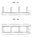
- FIGS. 3A through 3H are views to explain a method of manufacturing a display device according to an example embodiment.
- a transparent substrate 120 is prepared.
- Barrier ribs 141 for defining pixels are formed on the transparent substrate 120 .
- the transparent substrate 120 may be formed of glass or a transparent plastic material, and a TFT layer 130 including transistors for driving pixels may be formed on the transparent substrate 120 .
- a light absorption layer for absorbing light that is not used to form an image may be formed on a surface (e.g., a lower surface) of the transparent substrate 120 .
- a transparent substrate 160 is attached to the barrier ribs 141 .
- an adhesive (not shown) is coated on the barrier ribs 141 by micro contact printing, and the transparent substrate 160 is attached to the barrier ribs 141 via the adhesive.
- a liquid crystal composition 140 ′ is injected into a cell gap.
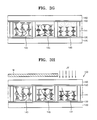
- the liquid crystal composition 140 ′ is prepared by dissolving a chiral dopant in a mixed solution containing an optically polymerizable polymer and a liquid crystal molecule.
- the optically polymerizable polymer may be an ultraviolet (UV) ray curable polymer such as an acrylate-based polymer, but is not limited thereto.
- the chiral dopant may be a generally known chiral compound that is mirror symmetric.
- the chiral dopant is dissolved until the mixed solution is supersaturated with the chiral dopant, and the amount of chiral dopant may be controlled such that the helix pitch of a cholesteric phase formed from the liquid crystal composition 140 ′ corresponds to red light. Because the solubility of the chiral dopant varies according to temperature, the temperature is controlled such that the amount of dissolved chiral dopant corresponds to the helix pitch of a cholesteric phase formed from the liquid crystal composition 140 ′ corresponding to the red light, while the supersaturation state of the chiral dopant is maintained in the liquid crystal composition 140 ′.
- the optically polymerizable polymer included in a portion of the liquid crystal composition 140 ′ corresponding to a first subpixel unit 143 is cured.
- the temperature set with reference to FIG. 3C is maintained constant or substantially constant.
- the first subpixel unit 143 is formed using a mask M that exposes only the portion of the liquid crystal composition 140 ′ corresponding to the first subpixel unit 143 to irradiation of ultraviolet (UV) rays.
- UV ultraviolet
- the temperature of the liquid crystal composition 140 ′ is raised to change the solubility of the chiral dopant. Because the solubility of the chiral dopant increases as the temperature is raised, the chiral dopant which is not dissolved due to the supersaturation is further dissolved. In general, when the amount of chiral dopant in the liquid crystal composition 140 ′ is increased, the helix pitch of the cholesteric phase is reduced. Thus, the temperature is controlled such that the amount of chiral dopant is adjusted to obtain a helix pitch that corresponds to a reflection wavelength range corresponding to green light. In this case, the temperature change does not affect the helix pitch of the first subpixel unit 143 that has been fixed by curing the optically polymerizable polymer.
- UV rays are irradiated through a mask M that exposes only a portion of the liquid crystal composition 140 ′ corresponding to a second subpixel unit 145 .
- the temperature used in the operation described with reference to FIG. 3E is maintained constant or substantially constant. In some cases, this operation may be performed together (e.g., concurrently or simultaneously) with the operation described with reference to FIG. 3E .
- the optically polymerizable polymer in the UV-exposed region is cured and a helix pitch is fixed, thereby forming the second subpixel unit 145 having the reflection wavelength range corresponding to green light.
- the mask M exposes only the portion of the liquid crystal composition 140 ′ corresponding to the second subpixel unit 145 , the mask M may also expose the first subpixel unit 143 because the reflection wavelength range of the first subpixel unit 143 that has been formed by curing with UV rays is not affected by additional irradiation of UV rays.
- the temperature of the liquid crystal composition 140 ′ is further raised to dissolve additional chiral dopant.
- the temperature is controlled such that the amount of chiral dopant is adjusted to obtain a helix pitch having a reflection wavelength range corresponding to blue light.
- the temperature change does not affect the helix pitches of the first subpixel unit 143 and second subpixel unit 145 , which have been fixed by curing the optically polymerizable polymer.
- UV rays are irradiated through a mask M that exposes only a portion of the liquid crystal composition 140 ′ corresponding to a third subpixel unit 147 .
- the temperature used in the operation described with reference to FIG. 3G is maintained constant or substantially constant. In some cases, this operation may be performed together with the operation described with reference to FIG. 3G .
- the optically polymerizable polymer in the UV-exposed region is cured and a helix pitch is fixed, thereby forming the third subpixel unit 147 having the reflection wavelength range corresponding to blue light.
- This operation may be performed without the mask M because the reflection wavelength ranges of the first subpixel unit 143 and second subpixel unit 145 , which have been formed by curing with UV rays, are not affected by additional irradiation of UV rays.
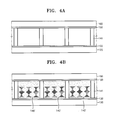
- FIGS. 4A through 4G are views to explain a method of manufacturing a display device according to another example embodiment.
- a light absorption layer for absorbing light may be formed on a surface of the transparent substrate 120 .
- the liquid crystal composition 140 ′ is injected into a cell gap.
- the liquid crystal composition 140 ′ is prepared by dissolving a chiral dopant in a mixed solution containing an optically polymerizable polymer and a liquid crystal molecule.
- the amount of dissolved chiral dopant may be controlled such that a helix pitch of a cholesteric phase formed from the liquid crystal composition 140 ′ corresponds to blue light.
- the optically polymerizable polymer contained in the portion of the liquid crystal composition 140 ′ corresponding to the third subpixel unit 147 is cured.
- the temperature is maintained constant or substantially constant.
- the third subpixel unit 147 is formed by irradiating UV rays through a mask M that exposes only the portion of the liquid crystal composition 140 ′ corresponding to the third subpixel unit 147 . Due to the irradiation of UV rays, the optically polymerizable polymer contained in the UV-exposed region is cured, and a helix pitch is fixed such that the reflection wavelength range corresponds to blue light.
- the temperature of the liquid crystal composition 140 ′ is lowered to change the solubility of the chiral dopant.
- the solubility of the chiral dopant is decreased as the temperature is lowered, and thus, some of the chiral dopant that has been dissolved is precipitated.
- a decrease in the amount of chiral dopant contained in the liquid crystal composition 140 ′ leads to a longer helix pitch of the cholesteric phase.
- the temperature is controlled such that the amount of chiral dopant is adjusted to obtain a helix pitch having a reflection wavelength range corresponding to the green light. In this case, lowering the temperature does not affect the helix pitch of the third subpixel unit 147 that has been fixed by curing the optically polymerizable polymer.
- UV rays are irradiated through a mask M that exposes only the portion of the liquid crystal composition 140 ′ corresponding to the second subpixel unit 145 .
- the temperature used in the operation described with reference to FIG. 4D is maintained constant or substantially constant. In some cases, this operation may be performed together (e.g., concurrently or simultaneously) with the operation described with reference to FIG. 4D .
- the optically polymerizable polymer in the UV-exposed region is cured and a helix pitch is fixed, thereby forming the second subpixel unit 145 having the reflection wavelength range corresponding to green light.
- the mask M exposes only the portion of the liquid crystal composition 140 ′ corresponding to the second subpixel unit 145 , the mask M may also expose the third subpixel unit 147 because the reflection wavelength range of the third subpixel unit 147 that has been formed by curing with UV rays is not affected by additional irradiation of UV rays.
- the temperature of the liquid crystal composition 140 ′ is further lowered to further precipitate the dissolved chiral dopant.
- the temperature is controlled such that the amount of chiral dopant is adjusted to obtain a helix pitch having a reflection wavelength range corresponding to red light.
- the temperature change does not affect the helix pitches of the second subpixel unit 145 and the third subpixel unit 147 , which have been fixed by curing the optically polymerizable polymer.
- UV rays are irradiated through a mask M that exposes only the portion of the liquid crystal composition 140 ′ corresponding to the first subpixel unit 143 .
- the temperature used in the operation described with reference to FIG. 4F is maintained constant or substantially constant. In some cases, this operation may be performed together (e.g., concurrently or simultaneously) with the operation described with reference to FIG. 4F .
- the optically polymerizable polymer in the UV-exposed region is cured and a helix pitch is fixed, thereby forming the first subpixel unit 143 having the reflection wavelength range corresponding to red light.
- This operation may be performed without the mask M because the second subpixel unit 145 and the third subpixel unit 147 , which have been formed by curing with UV rays, are not affected by the additional irradiation of UV rays.
- cholesteric liquid crystal display devices including a plurality of subpixel units having different reflection wavelength ranges is manufactured.
- the cholesteric liquid crystal display devices may include a single-layered liquid crystal layer. Due to the single-layered structure, manufacturing costs are relatively low and improved color purity is obtained.
- the operation of curing an optically polymerizable polymer contained in a cholesteric liquid crystal layer at different temperatures to form pixels for producing a full-color image is suitable for simplifying a structure process and mass production.
- a liquid crystal composition is processed to form a helix pitch corresponding to red light or blue light.
- the temperature is then raised or lowered (e.g., gradually raised or lowered).
- the embodiments described herein are examples only.
- the liquid crystal composition may also be processed to obtain a helix pitch corresponding to light of other colors, and the temperature may be raised or lowered according to operation requirements.
Landscapes
- Chemical & Material Sciences (AREA)
- Physics & Mathematics (AREA)
- Nonlinear Science (AREA)
- Crystallography & Structural Chemistry (AREA)
- Engineering & Computer Science (AREA)
- Materials Engineering (AREA)
- Organic Chemistry (AREA)
- General Physics & Mathematics (AREA)
- Optics & Photonics (AREA)
- Liquid Crystal (AREA)
- Liquid Crystal Substances (AREA)
Abstract
Description
Claims (5)
Applications Claiming Priority (2)
| Application Number | Priority Date | Filing Date | Title |
|---|---|---|---|
| KR1020090067011A KR101644582B1 (en) | 2009-07-22 | 2009-07-22 | Cholesteric liquid crystal display device and method of manufacturing the same |
| KR10-2009-0067011 | 2009-07-22 |
Publications (2)
| Publication Number | Publication Date |
|---|---|
| US20110019132A1 US20110019132A1 (en) | 2011-01-27 |
| US8456594B2 true US8456594B2 (en) | 2013-06-04 |
Family
ID=43497031
Family Applications (1)
| Application Number | Title | Priority Date | Filing Date |
|---|---|---|---|
| US12/659,558 Expired - Fee Related US8456594B2 (en) | 2009-07-22 | 2010-03-12 | Cholesteric liquid crystal display devices and methods of manufacturing the same |
Country Status (2)
| Country | Link |
|---|---|
| US (1) | US8456594B2 (en) |
| KR (1) | KR101644582B1 (en) |
Cited By (1)
| Publication number | Priority date | Publication date | Assignee | Title |
|---|---|---|---|---|
| US20120274883A1 (en) * | 2009-12-21 | 2012-11-01 | Ndis Corporation | Liquid crystal display device and manufacturing method thereof |
Families Citing this family (17)
| Publication number | Priority date | Publication date | Assignee | Title |
|---|---|---|---|---|
| JP2012133105A (en) * | 2010-12-21 | 2012-07-12 | Fujitsu Ltd | Method for manufacturing liquid crystal display element and liquid crystal display element |
| CN103176301A (en) * | 2011-12-21 | 2013-06-26 | 东莞万士达液晶显示器有限公司 | Reflective liquid crystal display device and manufacturing method thereof |
| CN102707481B (en) * | 2012-03-15 | 2016-01-13 | 京东方科技集团股份有限公司 | Display panels and preparation method thereof, liquid crystal display |
| CN102981323B (en) * | 2012-12-03 | 2015-02-04 | 京东方科技集团股份有限公司 | Display panel, manufacturing method thereof and display device |
| EP2963488A1 (en) * | 2014-06-30 | 2016-01-06 | LG Display Co., Ltd. | Light controlling apparatus and transparent display including the same |
| KR101624633B1 (en) | 2014-07-14 | 2016-05-26 | 부산대학교 산학협력단 | Bistable Cholesteric Liquid Crystal Display Device with Fast Response Time |
| KR20160022495A (en) * | 2014-08-20 | 2016-03-02 | 삼성전자주식회사 | Display apparatus and method for fabricating of the same |
| US20160098416A1 (en) * | 2014-10-03 | 2016-04-07 | Yahoo! Inc. | Auto complete search box based on the user's context to reduce user's input |
| KR20170000444U (en) | 2015-07-23 | 2017-02-02 | 대우조선해양 주식회사 | Anti-Impact device by the door opens for vessel |
| CN106997116B (en) * | 2017-04-28 | 2018-02-23 | 深圳市唯酷光电有限公司 | The preparation method and preparation facilities of the hand-written film of liquid crystal, the hand-written film of liquid crystal |
| KR20220124474A (en) * | 2021-03-03 | 2022-09-14 | 한양대학교 산학협력단 | Selective light reflection display and manufacturing method thereof |
| CN113589578A (en) * | 2021-07-23 | 2021-11-02 | Tcl华星光电技术有限公司 | Liquid crystal display device and method for manufacturing the same |
| CN114740651B (en) * | 2022-04-29 | 2024-05-28 | 南京大学 | A transmissive optical device and a method for preparing the same |
| CN115542598B (en) * | 2022-09-28 | 2023-09-19 | 惠科股份有限公司 | Electronic paper display and preparation method thereof |
| CN115586675B (en) * | 2022-09-28 | 2023-09-19 | 惠科股份有限公司 | Electronic paper display and preparation method thereof |
| KR20250033458A (en) | 2023-08-30 | 2025-03-10 | 이미지팹 주식회사 | Switching window panels using the driving characteristics of multiple reflective and transmissive panels |
| CN119322421B (en) * | 2024-10-23 | 2025-10-24 | Tcl华星光电技术有限公司 | Display panel and display device |
Citations (9)
| Publication number | Priority date | Publication date | Assignee | Title |
|---|---|---|---|---|
| US5798808A (en) * | 1994-08-23 | 1998-08-25 | U.S. Philips Corporation | Liquid crystal display device having a cholesteric order with a pitch of helix less than 0.25 microns and a retardation foil |
| US6143379A (en) * | 1997-04-17 | 2000-11-07 | Clariant Gmbh | Polymer laminates having increased hiding power |
| KR20020062188A (en) | 2001-01-18 | 2002-07-25 | 후지 샤신 필름 가부시기가이샤 | Method of producing a cholesteric liquid crystal color filter |
| KR20030010498A (en) | 2001-07-05 | 2003-02-05 | 다이니폰 인사츠 가부시키가이샤 | Process of producing multicolor optical element |
| KR20030017381A (en) | 2001-08-22 | 2003-03-03 | 후지 샤신 필름 가부시기가이샤 | Cholesteric liquid crystal color filter and method of producing the same |
| US6636291B2 (en) | 2000-06-06 | 2003-10-21 | Koninklijke Philips Electronics N.V. | Liquid crystal display device with patterned layer having fixed cholesteric order and method of manufacturing the same |
| US6735009B2 (en) * | 2002-07-16 | 2004-05-11 | Motorola, Inc. | Electroptic device |
| KR20040080322A (en) | 2001-11-12 | 2004-09-18 | 다이니폰 인사츠 가부시키가이샤 | Method for making circularly-polarized light control optical device |
| KR20080014094A (en) | 2007-12-28 | 2008-02-13 | 후지쯔 가부시끼가이샤 | Liquid crystal composition, liquid crystal display element using the same, and electronic paper having same |
Family Cites Families (3)
| Publication number | Priority date | Publication date | Assignee | Title |
|---|---|---|---|---|
| JP3118351B2 (en) * | 1993-10-19 | 2000-12-18 | シャープ株式会社 | Super twisted nematic liquid crystal display device and method of manufacturing the same |
| JP2000328051A (en) * | 1999-05-18 | 2000-11-28 | Dainippon Ink & Chem Inc | Liquid crystal optical element and optical switching method |
| KR20070002774A (en) * | 2005-06-30 | 2007-01-05 | 엘지.필립스 엘시디 주식회사 | LCD using cholesteric liquid crystal |
-
2009
- 2009-07-22 KR KR1020090067011A patent/KR101644582B1/en not_active Expired - Fee Related
-
2010
- 2010-03-12 US US12/659,558 patent/US8456594B2/en not_active Expired - Fee Related
Patent Citations (9)
| Publication number | Priority date | Publication date | Assignee | Title |
|---|---|---|---|---|
| US5798808A (en) * | 1994-08-23 | 1998-08-25 | U.S. Philips Corporation | Liquid crystal display device having a cholesteric order with a pitch of helix less than 0.25 microns and a retardation foil |
| US6143379A (en) * | 1997-04-17 | 2000-11-07 | Clariant Gmbh | Polymer laminates having increased hiding power |
| US6636291B2 (en) | 2000-06-06 | 2003-10-21 | Koninklijke Philips Electronics N.V. | Liquid crystal display device with patterned layer having fixed cholesteric order and method of manufacturing the same |
| KR20020062188A (en) | 2001-01-18 | 2002-07-25 | 후지 샤신 필름 가부시기가이샤 | Method of producing a cholesteric liquid crystal color filter |
| KR20030010498A (en) | 2001-07-05 | 2003-02-05 | 다이니폰 인사츠 가부시키가이샤 | Process of producing multicolor optical element |
| KR20030017381A (en) | 2001-08-22 | 2003-03-03 | 후지 샤신 필름 가부시기가이샤 | Cholesteric liquid crystal color filter and method of producing the same |
| KR20040080322A (en) | 2001-11-12 | 2004-09-18 | 다이니폰 인사츠 가부시키가이샤 | Method for making circularly-polarized light control optical device |
| US6735009B2 (en) * | 2002-07-16 | 2004-05-11 | Motorola, Inc. | Electroptic device |
| KR20080014094A (en) | 2007-12-28 | 2008-02-13 | 후지쯔 가부시끼가이샤 | Liquid crystal composition, liquid crystal display element using the same, and electronic paper having same |
Cited By (2)
| Publication number | Priority date | Publication date | Assignee | Title |
|---|---|---|---|---|
| US20120274883A1 (en) * | 2009-12-21 | 2012-11-01 | Ndis Corporation | Liquid crystal display device and manufacturing method thereof |
| US9019446B2 (en) * | 2009-12-21 | 2015-04-28 | Ndis Corporation | Liquid crystal display device and manufacturing method thereof |
Also Published As
| Publication number | Publication date |
|---|---|
| US20110019132A1 (en) | 2011-01-27 |
| KR101644582B1 (en) | 2016-08-02 |
| KR20110009557A (en) | 2011-01-28 |
Similar Documents
| Publication | Publication Date | Title |
|---|---|---|
| US8456594B2 (en) | Cholesteric liquid crystal display devices and methods of manufacturing the same | |
| US8749743B2 (en) | Cholesteric liquid crystal display devices and methods of manufacturing the same | |
| US8264637B2 (en) | Photonic crystal optical filter, reflective color filter, display apparatus using the reflective color filter, and method of manufacturing the reflective color filter | |
| US8363185B2 (en) | Photonic crystal optical filter, transmissive color filter, transflective color filter, and display apparatus using the color filters | |
| KR101636052B1 (en) | Color filter and display device employing the same | |
| US8264660B2 (en) | Polymer dispersed liquid crystal display with lateral light source and method of fabricating the same | |
| US20170108726A1 (en) | Liquid crystal display device | |
| US20170123267A1 (en) | Liquid crystal display device | |
| US11719983B2 (en) | Display panel, manufacturing method thereof and display device | |
| CN117215114A (en) | LCD device | |
| CN102099735A (en) | A stacked display with a bended substrate, an electronic apparatus and a method for manufacturing the same | |
| JP6856336B2 (en) | Liquid crystal display device and its manufacturing method | |
| CN103472515A (en) | Optical filter and manufacturing method and display device thereof | |
| KR20120063680A (en) | Reflective liquid crystal display device and method for manufacturing the same | |
| TWI280439B (en) | Liquid crystal display device | |
| CN117492283A (en) | a display panel | |
| TWI412792B (en) | Liquid crystal display device | |
| US20100091218A1 (en) | Color display | |
| US9019446B2 (en) | Liquid crystal display device and manufacturing method thereof | |
| US20060250566A1 (en) | Liquid crystal display | |
| JP5075326B2 (en) | Liquid crystal panel using cholesteric mixture | |
| TW201319706A (en) | Pixel structure | |
| KR20110094669A (en) | Liquid Crystal Display and Manufacturing Method Thereof | |
| JP2010039038A (en) | Display device | |
| JP2002023145A (en) | Liquid crystal display device |
Legal Events
| Date | Code | Title | Description |
|---|---|---|---|
| AS | Assignment |
Owner name: SAMSUNG ELECTRONICS CO., LTD., KOREA, REPUBLIC OF Free format text: ASSIGNMENT OF ASSIGNORS INTEREST;ASSIGNORS:JANG, JAE-EUN;JUNG, JAE-EUN;HWANG, KYU-YOUNG;AND OTHERS;REEL/FRAME:024121/0402 Effective date: 20100310 |
|
| AS | Assignment |
Owner name: SAMSUNG ELECTRONICS CO., LTD., KOREA, REPUBLIC OF Free format text: TO CORRECT ASSIGNEES LISTED AT REEL/FRAME NUMBER 024121/0402;ASSIGNORS:JANG, JAE-EUN;JUNG, JAE-EUN;HWANG, KYU-YOUNG;AND OTHERS;REEL/FRAME:024307/0466 Effective date: 20100310 Owner name: INDUSTRY-UNIVERSITY COOPERATION FOUNDATION HANYANG Free format text: TO CORRECT ASSIGNEES LISTED AT REEL/FRAME NUMBER 024121/0402;ASSIGNORS:JANG, JAE-EUN;JUNG, JAE-EUN;HWANG, KYU-YOUNG;AND OTHERS;REEL/FRAME:024307/0466 Effective date: 20100310 |
|
| STCF | Information on status: patent grant |
Free format text: PATENTED CASE |
|
| CC | Certificate of correction | ||
| FEPP | Fee payment procedure |
Free format text: PAYOR NUMBER ASSIGNED (ORIGINAL EVENT CODE: ASPN); ENTITY STATUS OF PATENT OWNER: LARGE ENTITY |
|
| FPAY | Fee payment |
Year of fee payment: 4 |
|
| MAFP | Maintenance fee payment |
Free format text: PAYMENT OF MAINTENANCE FEE, 8TH YEAR, LARGE ENTITY (ORIGINAL EVENT CODE: M1552); ENTITY STATUS OF PATENT OWNER: LARGE ENTITY Year of fee payment: 8 |
|
| FEPP | Fee payment procedure |
Free format text: MAINTENANCE FEE REMINDER MAILED (ORIGINAL EVENT CODE: REM.); ENTITY STATUS OF PATENT OWNER: LARGE ENTITY |
|
| LAPS | Lapse for failure to pay maintenance fees |
Free format text: PATENT EXPIRED FOR FAILURE TO PAY MAINTENANCE FEES (ORIGINAL EVENT CODE: EXP.); ENTITY STATUS OF PATENT OWNER: LARGE ENTITY |
|
| STCH | Information on status: patent discontinuation |
Free format text: PATENT EXPIRED DUE TO NONPAYMENT OF MAINTENANCE FEES UNDER 37 CFR 1.362 |
|
| FP | Lapsed due to failure to pay maintenance fee |
Effective date: 20250604 |