US8433932B2 - Power circuit, information processing apparatus, and power control method based on fixed frequency characteristic of control signal - Google Patents
Power circuit, information processing apparatus, and power control method based on fixed frequency characteristic of control signal Download PDFInfo
- Publication number
- US8433932B2 US8433932B2 US12/618,294 US61829409A US8433932B2 US 8433932 B2 US8433932 B2 US 8433932B2 US 61829409 A US61829409 A US 61829409A US 8433932 B2 US8433932 B2 US 8433932B2
- Authority
- US
- United States
- Prior art keywords
- power source
- frequency characteristic
- time
- power
- fixed frequency
- Prior art date
- Legal status (The legal status is an assumption and is not a legal conclusion. Google has not performed a legal analysis and makes no representation as to the accuracy of the status listed.)
- Expired - Fee Related, expires
Links
Images


Classifications
-
- G—PHYSICS
- G06—COMPUTING OR CALCULATING; COUNTING
- G06F—ELECTRIC DIGITAL DATA PROCESSING
- G06F1/00—Details not covered by groups G06F3/00 - G06F13/00 and G06F21/00
- G06F1/26—Power supply means, e.g. regulation thereof
-
- G—PHYSICS
- G06—COMPUTING OR CALCULATING; COUNTING
- G06F—ELECTRIC DIGITAL DATA PROCESSING
- G06F1/00—Details not covered by groups G06F3/00 - G06F13/00 and G06F21/00
- G06F1/26—Power supply means, e.g. regulation thereof
- G06F1/30—Means for acting in the event of power-supply failure or interruption, e.g. power-supply fluctuations
Definitions
- PCs personal computers
- CPUs central processing units
- the power consumption and the heating value of the CPUs have also been increasing in recent years causing a problem of how to keep the performances, the power consumption, and the heating value of the CPUs within predetermined bounds.
- control system arranged to reduce the power consumption by decreasing the voltage of a power source provided for the CPU has become commonplace.
- the control system may be used to increase the battery retaining time.
- the PC 10 is provided as a mobile PC, and includes a CPU 101 , a peripheral large scale integration (LSI) circuit 102 including a chip set or the like, a hard disk device (HDD), various input/output devices 103 including a hard disk device (HDD), a keyboard, etc., a universal serial bus (USB) connector 104 a , a local area network (LAN) connector 104 b , an external monitor output connector 104 c , an external power input unit 105 , a charging circuit 106 , various power sources 107 , and a CPU core power source 110 .
- LSI peripheral large scale integration
- the CPU 101 executes various calculation processings.
- the peripheral LSI circuit 102 controls information exchanged between the internal various input/output devices 103 based on instructions of the CPU 101 . Further, the peripheral LSI circuit 102 controls information exchanged between the PC 10 and various USB devices 23 , various communication devices 24 , and an external monitor 25 via the individual USB connector 104 a , LAN connector 104 b , and external monitor output connector 104 c.
- the external power input unit 105 distributes power supplied from an alternating current (AC) adapter 21 and/or an internal and/or external battery 22 to the charging circuit 106 , the various power sources 107 , and the CPU core power source 110 .
- the charging circuit 106 controls charging of the battery 22 .
- Each of the various power sources 107 supplies power to each of the components except the CPU 101 , so as to drive each of the components except the CPU 101 .
- the CPU core power source 110 includes a power control unit 111 , an oscillation circuit 118 , and a smoothing circuit 119 , and supplies power used to drive the CPU 101 .
- the oscillation circuit 118 includes an input capacitor and/or a field effect transistor (FET), and generates a clock pulse signal.
- the smoothing circuit 119 includes a coil and/or an output capacitor, smoothes the clock pulse signal, and supplies the smoothed clock pulse signal to the CPU 101 as power.
- the power control unit 111 includes a control signal input unit 112 , a digital-to-analog (D/A) converter 113 , a reference voltage generating unit 114 , an error amplifier unit 115 , a pulse width modulation (PWM) generating unit 116 , and a driver unit 117 , and controls the oscillation circuit 118 .
- D/A digital-to-analog
- PWM pulse width modulation
- the control signal input unit 112 receives a power voltage control signal transmitted from the CPU 101 .
- the D/A converter 113 converts the power voltage control signal into an analog signal
- the reference voltage generating unit 114 generates a reference voltage based on the power voltage control signal converted into the analog signal.
- the error amplifier unit 115 compares the reference voltage to a voltage transmitted from the smoothing circuit 119 , and transmits data of the difference between the above-described voltages.
- the PWM generating unit 116 transmits an oscillation control signal subjected to PWM modulation performed based on the magnitude of the data transmitted from the error amplifier unit 115 .
- the driver unit 117 drives the oscillation circuit 118 based on the oscillation control signal.
- interrupt processing may be periodically performed by recovering a voltage so as to control the various devices, for example, even though the voltage of the power source provided for the CPU 101 is reduced to some extent. Since the output capacitor may be provided with many electric charges so as to recover the voltage, a large current periodically occurs in the CPU core power source 110 .
- the print substrate is periodically vibrated. Then, if the period is an audible frequency, the print substrate functions as a speaker, and the sound of the frequency corresponding to the period is generated from the entire print substrate.
- the loudness of the above-described sound (hereinafter referred to as a “ringing sound”) generated due to the vibration of the print substrate is so high that a person can perceive the ringing sound, which is often offensive to the person.
- the ringing sound can be reduced to some extent by providing a specifically designed capacitor and/or a specifically designed coil as the above-described capacitor and coil.
- the reduction effect is often definitive and the parts used for the specifically designed capacitor and coil are often expensive.
- the reduction effect may be definitive. Further, being affected by other parts and/or wiring, the know-how to achieve the ringing sound reduction often becomes significantly difficult.
- a power circuit that includes a determining unit configured to determine whether a control signal provided to control a power source has a fixed frequency characteristic and an adjusting unit configured to randomly change time when a voltage transmitted to the power source is changed within a prescribed range when the determining unit determines that the control signal has the fixed frequency characteristic.
- FIG. 1 illustrates a PC
- FIG. 2 illustrates a power control method
- FIG. 3 illustrates a power control method according to a first embodiment.
- FIG. 4 illustrates an outer appearance of a PC according to the first embodiment.
- FIG. 5 illustrates a PC according to the first embodiment.
- FIG. 6 illustrates processing procedures performed through a frequency characteristic detecting unit.
- FIG. 7 illustrates an exemplary effect of a power control method.
- FIG. 8 illustrates an exemplary power control method.
- FIG. 9 illustrates an exemplary power control method.
- FIG. 10 illustrates an exemplary power control method according to a second embodiment.
- FIG. 11 illustrates an exemplary PC according to a second embodiment.
- FIG. 12 illustrates processing procedures performed through another frequency characteristic detecting unit.
- FIG. 13 illustrates an exemplary PC according to a second embodiment.
- FIG. 14 illustrates a PC
- FIG. 15 illustrates a power control method
- a PC may be used as an exemplary information processing apparatus executing an exemplary power control method.
- the power control method can be used for various information processing apparatuses including, for example, a mobile terminal such as a mobile phone and/or a communication device such as a router device.
- An above-described power control method allows for perceiving the periodicity of a power voltage control signal transmitted from a CPU. If the power voltage control signal has the periodicity, the time when the transmission of the power voltage control signal is started is moved up by as much as a random time.
- the control achieved by changing the period where a voltage transmitted to the CPU is changed is effective to reduce the ringing sound.
- the system may not be provided with a sufficient power under heavy load conditions so that the operations of the system become unstable. Since the power control method moves up the time when the transmission of the power voltage control signal is started, a sufficient amount of power is supplied when the CPU is in the active state so that the system can operate with stability.
- the moved-up time may be within a relatively narrow range.
- a method of using a random number generating function of the CPU, a method of detecting the temperature of a predetermined part and using fluctuations of the detected temperature, etc. can be considered as the method of determining the random moved-up time.
- a PC 40 executing the power control method is disclosed. Similar parts are designated by the same reference numerals so as to eliminate a repetition of the descriptions.
- FIG. 4 illustrates an outer appearance of PC 40 including a first unit 400 and a second unit 500 .
- the first unit 400 and the second unit 500 may be coupled to each other through a biaxial coupling unit 45 so that the second unit 500 can be freely opened and closed in a direction indicated by an arrow A-A with reference to the first unit 400 and freely rotated in a direction indicated by an arrow B-B (about a vertical rotation axis).
- FIG. 4 illustrates that the second unit 500 is opened to the first unit 400 (open state).
- the front face of the first unit 400 may be covered with an upper cover 93 on which a keyboard 421 , a track pad 422 , a left-click button 423 , a right-click button 424 , and a locking unit 425 are provided, where the locking unit 425 locks the second unit 500 when the second unit 500 is closed.
- the locking unit 425 includes a locking hole 451 into which a catch of the second unit 500 enters and a lock releasing button 452 provided to release the locking of the catch which had entered the locking hole 451 .
- the outer side face of the first unit 400 includes an open/close lid 461 of an optical disk drive 460 where an optical disk including a compact disk (CD), a digital versatile disk (DVD), and so forth is inserted into the optical disk drive 460 so that the optical disk drive 460 drives and accesses the optical disk.
- An eject button 462 may be provided on the open/close lid 461 , where the open/close lid 461 is opened by pressing the eject button 462 .
- the CPU 101 may be under the upper cover 93 of the first unit 400 .
- a cover 530 having a display window 531 may be provided on the front face of the second unit 500 of the PC 40 .
- An internal display panel 540 spreads over the display window 531 .
- a plurality of press buttons 532 may be provided under the display panel 540
- a catch unit 550 is provided at a part defined on the display panel 540 , where the catch unit 550 includes a catch which locks the locking unit 425 of the first unit 400 when the second unit 500 is closed.
- the catch unit 550 includes two catches and any one of the two catches, that is, a catch 552 a which sticks out from an opening 551 a provided on the display screen side.
- the PC 40 includes the CPU 101 , the peripheral LSI circuit 102 , the various input/output devices 103 , the USB connector 104 a , the LAN connector 104 b , the external monitor output connector 104 c , the external power input unit 105 , the charging circuit 106 , the various power sources 107 , and the CPU core power source 410 .
- the CPU core power source 410 includes a power control unit 411 , an oscillation circuit 118 , and the smoothing circuit 119 , and supplies power used to drive the CPU 101 .
- the power control unit 411 includes the control signal input unit 112 , a frequency characteristic detecting unit 412 , a buffer circuit 413 , a D/A converter 113 , the reference voltage generating unit 114 , the error amplifier unit 115 , the PWM generating unit 116 , and the driver unit 117 , and controls the oscillation circuit 118 .
- the frequency characteristic detecting unit 412 perceives the periodicity of a power voltage control signal transmitted to the control signal input unit 112 . If the power voltage control signal has the periodicity, the frequency characteristic detecting unit 412 moves up the time when the transmission of the power voltage control signal is started by as much as a random time.
- the buffer circuit 413 temporarily stores information used to detect the periodicity of the power voltage control signal.
- FIG. 6 illustrates processing procedures performed through the frequency characteristic detecting unit 412 illustrated in FIG. 5 .
- the maximum value of the moved-up time is determined to be 10% of the period.
- the frequency characteristic detecting unit 412 waits for the reception of an output control signal in a thread 1 at operation S 101 . Upon receiving the output control signal (Yes at operation S 101 ), the frequency characteristic detecting unit 412 starts a thread 2 , stops a timer, and notifies the thread 2 of the timer value as a counter value. The frequency characteristic detecting unit 412 transmits the output control signal and starts output voltage changing processing at operation S 102 . The frequency characteristic detecting unit 412 restarts the timer at operation S 103 and restarts the processing procedures from operation S 101 .
- the frequency characteristic detecting unit 412 compares the counter value acquired from the notification provided through the thread 1 and a counter value of which data had been stored in the buffer circuit 413 at operation S 201 . If the above-described counter values are not approximately equal to each other (No at operation S 201 ), it is considered that the power voltage control signal has no periodicity. Therefore, the frequency characteristic detecting unit 412 stores data of the counter value acquired from the notification provided through the thread 1 in the buffer circuit 413 at operation S 202 , and terminates the thread 2 without performing the moving-up processing at operation S 203 .
- the value “a” may represent a random number of which value is from 0 to 1
- the value “bt” may represent a counter value of which data had been stored in the buffer circuit 413 .
- the time attained by waiting by as much as the time T calculated through Equation (1) may be the time attained by moving up the time when the power voltage control signal is changed next time by as much as 0 to 10% of the counter value bt.
- the frequency characteristic detecting unit 412 determines whether a power voltage control signal of the next period is transmitted and processing for changing an output voltage is started at operation S 205 . If the power voltage control signal of the next period is transmitted (Yes at operation S 205 ), the periodicity had already been lost. Therefore, the frequency characteristic detecting unit 412 terminates the thread 2 without performing the moving-up processing at operation S 203 .
- the frequency characteristic detecting unit 412 performs the moving-up processing, transmits an output control signal, and starts the output voltage changing processing at operation S 206 . After that, the frequency characteristic detecting unit 412 terminates the thread 2 at operation S 203 .
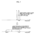
- FIG. 7 illustrates an effect obtained by using the power control method of the above-described embodiment, where the moved-up time is determined to be 100 ⁇ sec at the maximum, for an apparatus where the ringing sound corresponding to a frequency of 1 kHz or around is generated.
- the peak height of the frequency is proportional to the loudness of the ringing sound, and a loud ringing sound occurs before using the power control method of the above-described embodiment.
- the peak height is suppressed to less than 1/50 thereof so that the ringing sound is significantly reduced.
- the time when the power voltage control signal is transmitted is moved up so that the time when the output voltage is increased is randomly changed. Consequently, the loudness of the ringing sound can be reduced.
- the time when the power voltage control signal is transmitted may be moved up so that the time when the output voltage is increased is randomly changed.
- the time may be randomly delayed time when the transmission of the power voltage control signal is terminated so that the time when the output voltage is decreased is randomly delayed.
- the above-described exemplary configuration may be used in the case where a single periodicity is provided. However, if a plurality of periodicities is provided, an increased number of the buffer circuits 413 may be used so as to retain the counter value over a plurality of generations, and an increased number of patterns of the comparison performed at operation S 201 executed in the thread 2 may be provided.
- a high frequency of periodicity may be detected by analyzing the periodicities of the generations through discrete Fourier transform (DFT) and/or fast Fourier transform (FFT), where data of the periodicities is stored in the buffer circuit 413 .
- DFT discrete Fourier transform
- FFT fast Fourier transform
- a method of suppressing the amount of the large generated current by gently decreasing a through rate at which the output voltage is changed by as much as the moved-up time is also effective to decrease the loudness of the ringing sound, as illustrated in FIGS. 6 and 7 .
- the reason why the above-described method is effective is that the level of a current occurring when the voltage is recovered can be lowered by gently decreasing the through rate.
- FIG. 14 illustrates a PC 30 , which includes the switching power source.
- the PC 30 includes the CPU 101 , the peripheral LSI circuit 102 , the various input/output devices 103 , the USB connector 104 a , the LAN connector 104 b , the external monitor output connector 104 c , the external power input unit 105 , the charging circuit 106 , the various power sources 107 , and a power circuit 310 .
- the power circuit 310 corresponds to the switching power source, and includes a power control unit 311 , the oscillation circuit 118 , and the smoothing circuit 119 .
- the power control unit 311 includes a reference voltage generating unit 312 , an error amplifier unit 313 , a PWM generating unit 314 , and a driver unit 315 , and controls the oscillation circuit 118 .
- the reference voltage generating unit 312 generates a reference voltage.
- the error amplifier unit 313 compares the reference voltage to a voltage transmitted from the smoothing circuit 119 , and transmits data of the difference between the above-described voltages.
- the PWM generating unit 314 transmits an oscillation control signal subjected to PWM modulation performed based on the magnitude of the data transmitted from the error amplifier unit 313 .
- the oscillation control signal includes oscillation-ON information and oscillation-OFF information.
- the driver unit 315 drives the oscillation circuit 118 based on the oscillation control signal.
- the oscillation period of the switching power source illustrated in FIG. 14 is often changed due to a change in external factors, as illustrated in FIG. 15 . However, as long as the external factors are constant, the oscillation period is often kept constant. If the oscillation period is constant, a ringing sound may be generated because of the constant oscillation period.
- FIG. 10 is a diagram illustrating an exemplary a power control method. As illustrated in FIG. 10 , the loudness of the ringing sound can be decreased by changing the oscillation period.
- FIG. 11 illustrates PC 50 .
- the PC 50 includes the CPU 101 , the peripheral LSI circuit 102 , the various input/output devices 103 , the USB connector 104 a , the LAN connector 104 b , the external monitor output connector 104 c , the external power input unit 105 , the charging circuit 106 , the various power sources 107 , and a power circuit 510 .
- the power circuit 510 corresponds to the switching power source, and includes a power control unit 511 , the oscillation circuit 118 , and the smoothing circuit 119 .
- the power control unit 511 includes the reference voltage generating unit 312 , the error amplifier unit 313 , the PWM generating unit 314 , the driver unit 315 , a frequency characteristic detecting unit 512 , and a buffer circuit 513 , and controls the oscillation circuit 118 .
- the frequency characteristic detecting unit 512 perceives the periodicity of oscillation-ON information included in an oscillation control signal generated through the PWM generation unit 314 . If the oscillation-ON information has the periodicity, the frequency characteristic detecting unit 512 moves up and/or down the time when the oscillation-ON information is transmitted by as much as a random time.
- the buffer circuit 513 temporarily stores information used to detect the periodicity of the oscillation-ON information.
- FIG. 12 illustrates processing procedures performed through the frequency characteristic detecting unit 512 illustrated in FIG. 11 .
- the time when the oscillation-ON information is transmitted is moved up by as much as 10% of the period at the maximum.
- the frequency characteristic detecting unit 512 waits for the reception of the oscillation-ON information in a thread 1 at operation S 301 . Upon receiving the oscillation-ON information (Yes at operation S 301 ), the frequency characteristic detecting unit 512 starts a thread 2 , stops a timer, and notifies the thread 2 of the timer value as a counter value. The frequency characteristic detecting unit 512 transmits the oscillation-ON information to be adjusted, as it is, as adjusted oscillation-ON information at operation S 302 . Next, the frequency characteristic detecting unit 512 restarts the timer at operation S 303 and restarts the processing procedures from operation 8301 .
- the frequency characteristic detecting unit 512 compares the counter value acquired from the notification provided through the thread 1 and a counter value of which data had been stored in the buffer circuit 513 at operation S 401 . If the above-described counter values are not approximately equal to each other (No at operation S 401 ), it is considered that the oscillation-ON information has no periodicity. Therefore, the frequency characteristic detecting unit 512 stores data of the counter value acquired from the notification provided through the thread 1 in the buffer circuit 513 at operation S 402 , and terminates the thread 2 without performing the moving-up processing at operation S 403 .
- the frequency characteristic detecting unit 512 waits by as much as the time T calculated through Equation (1) described above at operation S 404 .
- the frequency characteristic detecting unit 512 determines whether oscillation-ON information of the next period is transmitted and processing for changing an output voltage is started at operation S 405 . If the oscillation-ON information of the next period is transmitted (Yes at operation S 405 ), the periodicity had already been lost. Therefore, the frequency characteristic detecting unit 512 terminates the thread 2 without performing the moving-up processing at operation S 403 .
- the frequency characteristic detecting unit 512 performs the moving-up processing and transmits the oscillation-ON information at operation S 406 , and terminates the thread 2 at operation S 403 .
- the time when the oscillation-ON information is transmitted is adjusted so that the time when the output voltage is increased is randomly changed. Consequently, the loudness of the ringing sound can be reduced.
- the power control method can be used for a PC 51 illustrated in FIG. 13 , where the unadjusted oscillation-ON information of the PC 51 is supplied from a pulse generator 524 provided outside the power circuit 520 .
- the frequency characteristic detecting unit 522 corresponding to the frequency characteristic detecting unit 512 illustrated in FIG. 11 detects the periodicity of the oscillation-ON information supplied from the pulse generator 524 through the buffer circuit 523 , and adjusts the periodicity so that the time when the oscillation-ON information is transmitted becomes random.
- An exemplary power control method may be used in analog-form power circuit and/or in a digital-form power circuit.
- the embodiments can be implemented in computing hardware (computing apparatus) and/or software, such as (in a non-limiting example) any computer that can store, retrieve, process and/or output data and/or communicate with other computers.
- the results produced can be displayed on a display of the computing hardware.
- a program/software implementing the embodiments may be recorded on computer-readable media comprising computer-readable recording media.
- the program/software implementing the embodiments may also be transmitted over transmission communication media.
- Examples of the computer-readable recording media include a magnetic recording apparatus, an optical disk, a magneto-optical disk, and/or a semiconductor memory (for example, RAM, ROM, etc.).
- Examples of the magnetic recording apparatus include a hard disk device (HDD), a flexible disk (FD), and a magnetic tape (MT).
- optical disk examples include a DVD (Digital Versatile Disc), a DVD-RAM, a CD-ROM (Compact Disc-Read Only Memory), and a CD-R (Recordable)/RW.
- communication media includes a carrier-wave signal.
Landscapes
- Engineering & Computer Science (AREA)
- Theoretical Computer Science (AREA)
- Physics & Mathematics (AREA)
- General Engineering & Computer Science (AREA)
- General Physics & Mathematics (AREA)
- Power Sources (AREA)
- Dc-Dc Converters (AREA)
Abstract
Description
T=bt×(1−10/100×a) Equation (1)
Claims (17)
Applications Claiming Priority (2)
| Application Number | Priority Date | Filing Date | Title |
|---|---|---|---|
| JP2008-318683 | 2008-12-15 | ||
| JP2008318683A JP5088311B2 (en) | 2008-12-15 | 2008-12-15 | Power supply circuit, information processing apparatus, and power supply control method |
Publications (2)
| Publication Number | Publication Date |
|---|---|
| US20100153753A1 US20100153753A1 (en) | 2010-06-17 |
| US8433932B2 true US8433932B2 (en) | 2013-04-30 |
Family
ID=42242013
Family Applications (1)
| Application Number | Title | Priority Date | Filing Date |
|---|---|---|---|
| US12/618,294 Expired - Fee Related US8433932B2 (en) | 2008-12-15 | 2009-11-13 | Power circuit, information processing apparatus, and power control method based on fixed frequency characteristic of control signal |
Country Status (2)
| Country | Link |
|---|---|
| US (1) | US8433932B2 (en) |
| JP (1) | JP5088311B2 (en) |
Cited By (1)
| Publication number | Priority date | Publication date | Assignee | Title |
|---|---|---|---|---|
| US10409207B2 (en) * | 2016-03-10 | 2019-09-10 | Ricoh Company, Ltd. | Transmission control apparatus and image forming apparatus with transmission control apparatus |
Families Citing this family (3)
| Publication number | Priority date | Publication date | Assignee | Title |
|---|---|---|---|---|
| JP5039215B2 (en) * | 2011-02-23 | 2012-10-03 | 株式会社東芝 | Noise reduction circuit, electronic device, noise reduction method |
| JP6490879B2 (en) * | 2016-12-06 | 2019-03-27 | パナソニック インテレクチュアル プロパティ コーポレーション オブ アメリカPanasonic Intellectual Property Corporation of America | Information processing apparatus and information processing method |
| JP6677891B2 (en) * | 2017-07-24 | 2020-04-08 | 富士通クライアントコンピューティング株式会社 | Information processing apparatus and voltage control method |
Citations (6)
| Publication number | Priority date | Publication date | Assignee | Title |
|---|---|---|---|---|
| JP2001125691A (en) | 1999-10-28 | 2001-05-11 | Toshiba Corp | Computer and CPU intermittent operation control method |
| US6510068B1 (en) * | 2001-07-17 | 2003-01-21 | Douglas A. Bors | Pulse width modulation utilizing a shifted control signal |
| JP2006023645A (en) | 2004-07-09 | 2006-01-26 | Sharp Corp | Display device and driving method thereof |
| JP2006288104A (en) | 2005-04-01 | 2006-10-19 | Denso Corp | Switching apparatus |
| US7684462B2 (en) * | 2005-03-30 | 2010-03-23 | On-Bright Electronics (Shanghai) Co., Ltd. | System and method for controlling variations of switching frequency |
| US7948187B2 (en) * | 2007-05-22 | 2011-05-24 | Apple Inc. | Electronically controlling acoustic energy from piezoelectric transformers |
Family Cites Families (9)
| Publication number | Priority date | Publication date | Assignee | Title |
|---|---|---|---|---|
| JP3229019B2 (en) * | 1992-06-23 | 2001-11-12 | 東洋電機製造株式会社 | PWM inverter device |
| JPH07245942A (en) * | 1994-03-08 | 1995-09-19 | Yokogawa Electric Corp | Random switching power supply |
| JP3061049B1 (en) * | 1999-04-09 | 2000-07-10 | 株式会社村田製作所 | Piezoelectric transformer inverter |
| JP2003324944A (en) * | 2002-05-08 | 2003-11-14 | Fuji Electric Co Ltd | Power circuit |
| JP2005168129A (en) * | 2003-12-01 | 2005-06-23 | Toyota Industries Corp | Switching power supply circuit |
| JP2005274742A (en) * | 2004-03-23 | 2005-10-06 | Mitsubishi Electric Corp | Power supply for video display equipment |
| JP4525311B2 (en) * | 2004-11-25 | 2010-08-18 | パナソニック株式会社 | Switching power supply |
| JP4976797B2 (en) * | 2005-09-29 | 2012-07-18 | クラリオン株式会社 | Switching power supply |
| JP2007215317A (en) * | 2006-02-09 | 2007-08-23 | Seiko Instruments Inc | Switching power supply |
-
2008
- 2008-12-15 JP JP2008318683A patent/JP5088311B2/en not_active Expired - Fee Related
-
2009
- 2009-11-13 US US12/618,294 patent/US8433932B2/en not_active Expired - Fee Related
Patent Citations (6)
| Publication number | Priority date | Publication date | Assignee | Title |
|---|---|---|---|---|
| JP2001125691A (en) | 1999-10-28 | 2001-05-11 | Toshiba Corp | Computer and CPU intermittent operation control method |
| US6510068B1 (en) * | 2001-07-17 | 2003-01-21 | Douglas A. Bors | Pulse width modulation utilizing a shifted control signal |
| JP2006023645A (en) | 2004-07-09 | 2006-01-26 | Sharp Corp | Display device and driving method thereof |
| US7684462B2 (en) * | 2005-03-30 | 2010-03-23 | On-Bright Electronics (Shanghai) Co., Ltd. | System and method for controlling variations of switching frequency |
| JP2006288104A (en) | 2005-04-01 | 2006-10-19 | Denso Corp | Switching apparatus |
| US7948187B2 (en) * | 2007-05-22 | 2011-05-24 | Apple Inc. | Electronically controlling acoustic energy from piezoelectric transformers |
Cited By (1)
| Publication number | Priority date | Publication date | Assignee | Title |
|---|---|---|---|---|
| US10409207B2 (en) * | 2016-03-10 | 2019-09-10 | Ricoh Company, Ltd. | Transmission control apparatus and image forming apparatus with transmission control apparatus |
Also Published As
| Publication number | Publication date |
|---|---|
| JP5088311B2 (en) | 2012-12-05 |
| JP2010140421A (en) | 2010-06-24 |
| US20100153753A1 (en) | 2010-06-17 |
Similar Documents
| Publication | Publication Date | Title |
|---|---|---|
| KR101798269B1 (en) | Adaptive audio feedback system and method | |
| US8989406B2 (en) | User profile based audio adjustment techniques | |
| CN101051823B (en) | Portable audio equipment that provides automatic control of audio volume parameters for hearing protection | |
| US8433932B2 (en) | Power circuit, information processing apparatus, and power control method based on fixed frequency characteristic of control signal | |
| US20040109271A1 (en) | ESD protection circuit | |
| US20040264938A1 (en) | Audio event detection recording apparatus and method | |
| JP4078644B2 (en) | Information processing apparatus and method, and program | |
| EP3739429A1 (en) | Method and system for optimizing a core voltage level and operating frequency of individual subcomponents for reducing power consumption within a portable computing device | |
| WO2016074355A1 (en) | Terminal and control method and apparatus therefor, and storage medium | |
| US20200045417A1 (en) | Pop Sound Suppression Method, Audio Output Circuit, and Terminal | |
| US20060075166A1 (en) | Multiple function integrated circuit | |
| US20040208327A1 (en) | Microphone bias circuit | |
| JP3924544B2 (en) | Information processing apparatus, control method, program, and recording medium | |
| US20090161887A1 (en) | Data processing apparatus and method of controlling the same | |
| CN112367099A (en) | Clock signal processing method and device and electronic equipment | |
| JP4388117B2 (en) | Information processing apparatus and power supply control method | |
| JP4469758B2 (en) | Audio processing device | |
| CN115279134A (en) | Device fan speed control method, device, electronic device and readable storage medium | |
| US9385593B2 (en) | Suspend mode in charge pump | |
| US7046530B2 (en) | Method and apparatus for current limiting of an output of a DC-to-DC converter | |
| WO2017206495A1 (en) | Method and controlling apparatus for controlling application of electronic apparatus | |
| CN117130454A (en) | Power consumption adjustment method and electronic device | |
| WO2023038685A1 (en) | Dynamic configuration of spur cancellation | |
| KR20130063374A (en) | Mobile terminal and control method thereof | |
| US7219027B1 (en) | Operation monitor device for hardware component |
Legal Events
| Date | Code | Title | Description |
|---|---|---|---|
| AS | Assignment |
Owner name: FUJITSU LIMITED,JAPAN Free format text: ASSIGNMENT OF ASSIGNORS INTEREST;ASSIGNOR:NAKAZAWA, SHIGEAKI;REEL/FRAME:023533/0284 Effective date: 20091104 Owner name: FUJITSU LIMITED, JAPAN Free format text: ASSIGNMENT OF ASSIGNORS INTEREST;ASSIGNOR:NAKAZAWA, SHIGEAKI;REEL/FRAME:023533/0284 Effective date: 20091104 |
|
| STCF | Information on status: patent grant |
Free format text: PATENTED CASE |
|
| CC | Certificate of correction | ||
| FEPP | Fee payment procedure |
Free format text: PAYOR NUMBER ASSIGNED (ORIGINAL EVENT CODE: ASPN); ENTITY STATUS OF PATENT OWNER: LARGE ENTITY |
|
| FPAY | Fee payment |
Year of fee payment: 4 |
|
| AS | Assignment |
Owner name: FUJITSU CLIENT COMPUTING LIMITED, JAPAN Free format text: ASSIGNMENT OF ASSIGNORS INTEREST;ASSIGNOR:FUJITSU LIMITED;REEL/FRAME:048751/0065 Effective date: 20181128 |
|
| MAFP | Maintenance fee payment |
Free format text: PAYMENT OF MAINTENANCE FEE, 8TH YEAR, LARGE ENTITY (ORIGINAL EVENT CODE: M1552); ENTITY STATUS OF PATENT OWNER: LARGE ENTITY Year of fee payment: 8 |
|
| FEPP | Fee payment procedure |
Free format text: MAINTENANCE FEE REMINDER MAILED (ORIGINAL EVENT CODE: REM.); ENTITY STATUS OF PATENT OWNER: LARGE ENTITY |
|
| LAPS | Lapse for failure to pay maintenance fees |
Free format text: PATENT EXPIRED FOR FAILURE TO PAY MAINTENANCE FEES (ORIGINAL EVENT CODE: EXP.); ENTITY STATUS OF PATENT OWNER: LARGE ENTITY |
|
| STCH | Information on status: patent discontinuation |
Free format text: PATENT EXPIRED DUE TO NONPAYMENT OF MAINTENANCE FEES UNDER 37 CFR 1.362 |
|
| FP | Lapsed due to failure to pay maintenance fee |
Effective date: 20250430 |