US8418357B2 - Printed circuit board layout method - Google Patents
Printed circuit board layout method Download PDFInfo
- Publication number
- US8418357B2 US8418357B2 US12/329,614 US32961408A US8418357B2 US 8418357 B2 US8418357 B2 US 8418357B2 US 32961408 A US32961408 A US 32961408A US 8418357 B2 US8418357 B2 US 8418357B2
- Authority
- US
- United States
- Prior art keywords
- conducting portions
- pair
- portions
- component
- conducting
- Prior art date
- Legal status (The legal status is an assumption and is not a legal conclusion. Google has not performed a legal analysis and makes no representation as to the accuracy of the status listed.)
- Active, expires
Links
- 238000000034 method Methods 0.000 title claims abstract description 12
- 230000008878 coupling Effects 0.000 claims abstract description 17
- 238000010168 coupling process Methods 0.000 claims abstract description 17
- 238000005859 coupling reaction Methods 0.000 claims abstract description 17
- 239000003990 capacitor Substances 0.000 claims description 5
- 230000005540 biological transmission Effects 0.000 description 11
- 229910000679 solder Inorganic materials 0.000 description 1
Images


Classifications
-
- H—ELECTRICITY
- H05—ELECTRIC TECHNIQUES NOT OTHERWISE PROVIDED FOR
- H05K—PRINTED CIRCUITS; CASINGS OR CONSTRUCTIONAL DETAILS OF ELECTRIC APPARATUS; MANUFACTURE OF ASSEMBLAGES OF ELECTRICAL COMPONENTS
- H05K1/00—Printed circuits
- H05K1/02—Details
- H05K1/0286—Programmable, customizable or modifiable circuits
- H05K1/0295—Programmable, customizable or modifiable circuits adapted for choosing between different types or different locations of mounted components
-
- H—ELECTRICITY
- H05—ELECTRIC TECHNIQUES NOT OTHERWISE PROVIDED FOR
- H05K—PRINTED CIRCUITS; CASINGS OR CONSTRUCTIONAL DETAILS OF ELECTRIC APPARATUS; MANUFACTURE OF ASSEMBLAGES OF ELECTRICAL COMPONENTS
- H05K1/00—Printed circuits
- H05K1/02—Details
- H05K1/0213—Electrical arrangements not otherwise provided for
- H05K1/0216—Reduction of cross-talk, noise or electromagnetic interference
- H05K1/023—Reduction of cross-talk, noise or electromagnetic interference using auxiliary mounted passive components or auxiliary substances
- H05K1/0231—Capacitors or dielectric substances
-
- H—ELECTRICITY
- H05—ELECTRIC TECHNIQUES NOT OTHERWISE PROVIDED FOR
- H05K—PRINTED CIRCUITS; CASINGS OR CONSTRUCTIONAL DETAILS OF ELECTRIC APPARATUS; MANUFACTURE OF ASSEMBLAGES OF ELECTRICAL COMPONENTS
- H05K1/00—Printed circuits
- H05K1/02—Details
- H05K1/0213—Electrical arrangements not otherwise provided for
- H05K1/0237—High frequency adaptations
- H05K1/0243—Printed circuits associated with mounted high frequency components
-
- H—ELECTRICITY
- H05—ELECTRIC TECHNIQUES NOT OTHERWISE PROVIDED FOR
- H05K—PRINTED CIRCUITS; CASINGS OR CONSTRUCTIONAL DETAILS OF ELECTRIC APPARATUS; MANUFACTURE OF ASSEMBLAGES OF ELECTRICAL COMPONENTS
- H05K1/00—Printed circuits
- H05K1/02—Details
- H05K1/11—Printed elements for providing electric connections to or between printed circuits
- H05K1/111—Pads for surface mounting, e.g. lay-out
- H05K1/112—Pads for surface mounting, e.g. lay-out directly combined with via connections
- H05K1/113—Via provided in pad; Pad over filled via
-
- H—ELECTRICITY
- H05—ELECTRIC TECHNIQUES NOT OTHERWISE PROVIDED FOR
- H05K—PRINTED CIRCUITS; CASINGS OR CONSTRUCTIONAL DETAILS OF ELECTRIC APPARATUS; MANUFACTURE OF ASSEMBLAGES OF ELECTRICAL COMPONENTS
- H05K2201/00—Indexing scheme relating to printed circuits covered by H05K1/00
- H05K2201/09—Shape and layout
- H05K2201/09209—Shape and layout details of conductors
- H05K2201/09218—Conductive traces
- H05K2201/09236—Parallel layout
-
- H—ELECTRICITY
- H05—ELECTRIC TECHNIQUES NOT OTHERWISE PROVIDED FOR
- H05K—PRINTED CIRCUITS; CASINGS OR CONSTRUCTIONAL DETAILS OF ELECTRIC APPARATUS; MANUFACTURE OF ASSEMBLAGES OF ELECTRICAL COMPONENTS
- H05K2201/00—Indexing scheme relating to printed circuits covered by H05K1/00
- H05K2201/09—Shape and layout
- H05K2201/09818—Shape or layout details not covered by a single group of H05K2201/09009 - H05K2201/09809
- H05K2201/09954—More mounting possibilities, e.g. on same place of PCB, or by using different sets of edge pads
-
- H—ELECTRICITY
- H05—ELECTRIC TECHNIQUES NOT OTHERWISE PROVIDED FOR
- H05K—PRINTED CIRCUITS; CASINGS OR CONSTRUCTIONAL DETAILS OF ELECTRIC APPARATUS; MANUFACTURE OF ASSEMBLAGES OF ELECTRICAL COMPONENTS
- H05K2201/00—Indexing scheme relating to printed circuits covered by H05K1/00
- H05K2201/10—Details of components or other objects attached to or integrated in a printed circuit board
- H05K2201/10431—Details of mounted components
- H05K2201/10507—Involving several components
- H05K2201/10545—Related components mounted on both sides of the PCB
-
- H—ELECTRICITY
- H05—ELECTRIC TECHNIQUES NOT OTHERWISE PROVIDED FOR
- H05K—PRINTED CIRCUITS; CASINGS OR CONSTRUCTIONAL DETAILS OF ELECTRIC APPARATUS; MANUFACTURE OF ASSEMBLAGES OF ELECTRICAL COMPONENTS
- H05K2201/00—Indexing scheme relating to printed circuits covered by H05K1/00
- H05K2201/10—Details of components or other objects attached to or integrated in a printed circuit board
- H05K2201/10613—Details of electrical connections of non-printed components, e.g. special leads
- H05K2201/10621—Components characterised by their electrical contacts
- H05K2201/10636—Leadless chip, e.g. chip capacitor or resistor
-
- H—ELECTRICITY
- H05—ELECTRIC TECHNIQUES NOT OTHERWISE PROVIDED FOR
- H05K—PRINTED CIRCUITS; CASINGS OR CONSTRUCTIONAL DETAILS OF ELECTRIC APPARATUS; MANUFACTURE OF ASSEMBLAGES OF ELECTRICAL COMPONENTS
- H05K2201/00—Indexing scheme relating to printed circuits covered by H05K1/00
- H05K2201/10—Details of components or other objects attached to or integrated in a printed circuit board
- H05K2201/10613—Details of electrical connections of non-printed components, e.g. special leads
- H05K2201/10621—Components characterised by their electrical contacts
- H05K2201/10689—Leaded Integrated Circuit [IC] package, e.g. dual-in-line [DIL]
-
- Y—GENERAL TAGGING OF NEW TECHNOLOGICAL DEVELOPMENTS; GENERAL TAGGING OF CROSS-SECTIONAL TECHNOLOGIES SPANNING OVER SEVERAL SECTIONS OF THE IPC; TECHNICAL SUBJECTS COVERED BY FORMER USPC CROSS-REFERENCE ART COLLECTIONS [XRACs] AND DIGESTS
- Y02—TECHNOLOGIES OR APPLICATIONS FOR MITIGATION OR ADAPTATION AGAINST CLIMATE CHANGE
- Y02P—CLIMATE CHANGE MITIGATION TECHNOLOGIES IN THE PRODUCTION OR PROCESSING OF GOODS
- Y02P70/00—Climate change mitigation technologies in the production process for final industrial or consumer products
- Y02P70/50—Manufacturing or production processes characterised by the final manufactured product
-
- Y—GENERAL TAGGING OF NEW TECHNOLOGICAL DEVELOPMENTS; GENERAL TAGGING OF CROSS-SECTIONAL TECHNOLOGIES SPANNING OVER SEVERAL SECTIONS OF THE IPC; TECHNICAL SUBJECTS COVERED BY FORMER USPC CROSS-REFERENCE ART COLLECTIONS [XRACs] AND DIGESTS
- Y10—TECHNICAL SUBJECTS COVERED BY FORMER USPC
- Y10T—TECHNICAL SUBJECTS COVERED BY FORMER US CLASSIFICATION
- Y10T29/00—Metal working
- Y10T29/49—Method of mechanical manufacture
- Y10T29/49002—Electrical device making
- Y10T29/49117—Conductor or circuit manufacturing
- Y10T29/49124—On flat or curved insulated base, e.g., printed circuit, etc.
- Y10T29/4913—Assembling to base an electrical component, e.g., capacitor, etc.
Definitions
- the invention relates to layout of a circuit board and, more particularly, to a printed circuit board and layout method thereof.
- Printed circuit boards are designed for coupling control chips and electronic devices in two alternative modes to transmit signals such as high-speed differential signals.
- a commonly used printed circuit board 1 includes a pair of first transmission lines 11 A, 11 B, a pair of second transmission lines 12 A, 12 B, and a pair of third transmission lines 13 A, 13 B sequentially arranged thereon.
- a control chip 14 in a first coupling mode, is coupled to the first transmission lines 11 A, 11 B, and a first electronic device 15 is coupled between the second transmission lines 12 A, 12 B, and the first transmission lines 11 A, 11 B.
- the control chip 14 generates a pair of high-speed signals S 1 , S 2 such as high-speed differential signals. However, a circuit stub is thus created. Referring to FIG.
- the control chip 14 in a second coupling mode, is coupled to the first transmission lines 11 A, 11 B, a second electronic device 16 is coupled to ends of the third transmission lines 13 A, 13 B away from the control chip 14 , and a pair of resistors R 1 , R 2 must be added to connect with the second transmission lines 12 A, 12 B and the third transmission lines 13 A, 13 B. Cost of the printed circuit board 1 is increased accordingly.
- FIG. 1 is an exploded, isometric view of a printed circuit board in a first coupling mode, in accordance with an embodiment.
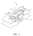
- FIG. 2 is an exploded, isometric view of the printed circuit board of FIG. 1 in a second coupling mode.
- FIGS. 3A , 3 B are flowcharts of a printed circuit board layout method for a printed circuit board in accordance with an embodiment.
- FIG. 4 is a schematic view of a commonly used printed circuit board.
- FIG. 5 is a schematic view of the commonly used printed circuit board of FIG. 4 , showing a first electronic device coupled therewith.
- FIG. 6 is a schematic view of the commonly used printed circuit board of FIG. 4 , showing a second electronic device coupled therewith.
- an embodiment of a printed circuit board 2 comprises an electronic device 4 , a first component 21 , and a second component 22 coupled thereto in two alternate coupling modes.
- the printed circuit board 2 also includes a first layout layer 24 , a second layout layer 23 , an isolating layer (not shown) disposed between the first layout layer 24 and the second layout layer 23 , a pair of connecting portions 29 A, 29 B, and a control chip 3 .
- the printed circuit board 2 can be, for example, a motherboard.
- the first layout layer 24 includes a pair of first parallel conducting portions 25 A, 25 B, such as, a pair of solder pads.
- the second layout layer 23 includes a pair of second parallel conducting portions 26 A, 26 B, a pair of third parallel conducting portions 27 A, 27 B, and a pair of fourth parallel conducting portions 28 A, 28 B, sequentially arranged on the second layout layer 23 in corresponding linear alignments.
- the third conducting portions 27 A, 27 B are coupled with the first conducting portions 25 A, 25 B, respectively, by the connecting portions 29 A, 29 B.
- the connecting portions 29 A, 29 B are a pair of vias or embedded vias.
- the first component 21 and the second component 22 can be capacitors or resistors.
- the first component 21 and the second component 22 are alternating current (AC) coupling capacitors.
- the control chip 3 is coupled with the first conducting portions 25 A, 25 B and generates a pair of high-speed differential signals S 3 , S 4 .
- the high-speed signals S 3 , S 4 are transmitted to the third conducting portions 27 A, 27 B by the first conducting portions 25 A, 25 B via a pair of transmission lines (not labeled).
- the electronic device 4 is coupled with the second conducting portions 26 A, 26 B. Two ends of the first component 21 are coupled with one of the second conducting portions 26 A and one of the third conducting portions 27 A. Two ends of the second component 22 are coupled with the other second conducting portion 26 B and the other third conducting portion 27 B.
- the high-speed signals S 3 , S 4 are transmitted to the electronic device 4 , sequentially passing through the first conducting portions 25 A, 25 B, the connecting portions 29 A, 29 B, the third conducting portions 27 A, 27 B, the first component 21 , the second component 22 , and the second conducting portions 26 A, 26 B.
- the electronic device 4 is coupled with the fourth conducting portions 28 A, 28 B.
- Two ends of the first component 21 are coupled with one of the third conducting portions 27 A and one of the fourth conducting portions 28 A.
- Two ends of the second component 22 are coupled with one of the third conducting portions 27 B and one of the fourth conducting portions 28 B.
- the control chip 3 remains coupled with the first conducting portions 25 A, 25 B.
- the high-speed signals S 3 , S 4 are transmitted to the electronic device 4 , sequentially passing through the first conducting portions 25 A, 25 B, the connecting portions 29 A, 29 B, the third conducting portions 27 A, 27 B, the first component 21 , the second component 22 , and the fourth conducting portions 28 A, 28 B.
- the printed circuit board layout method includes, in step S 01 , providing a printed circuit board 2 with a first layout layer 24 , and a second layout layer 23 .
- step S 02 a pair of first conducting portions 25 A, 25 B is disposed on a first layout layer 24 of the printed circuit board 2 to couple with a control chip.
- step S 03 a pair of second conducting portions 26 A, 26 B, third conducting portions 27 A, 27 B, and fourth conducting portions 28 A, 28 B are sequentially disposed on a second layout layer 23 of the printed circuit board 2 in corresponding linear alignments.
- step S 04 a pair of connecting portions 29 A, 29 B is coupled with the third conducting portions 27 A, 27 B and the first conducting portions 25 A, 25 B, respectively.
- step S 05 in a first coupling mode, an electronic device 4 is coupled with the second conducting portions 26 A, 26 B, a first component 21 is coupled with one of the second conducting portions 26 A and one of the third conducting portions 27 A, and a second component 22 is coupled with the other second conducting portion 26 B and the other third conducting portion 27 B.
- step S 06 in a second coupling mode, the electronic device 4 is coupled with the fourth conducting portions 28 A, 28 B, the first component 21 is coupled with one of the third conducting portions 27 A and one of the fourth conducting portions 28 A, and the second component 22 is coupled with the other third conducting portion 27 B and the other fourth conducting portion 28 B.
- the printed circuit board 2 positions the first component 21 and the second component 22 and the electronic device 4 in two different coupling modes. In this way, it is unnecessary for the printed circuit board 2 to bear additional components to satisfy two alternative coupling positions.
Landscapes
- Engineering & Computer Science (AREA)
- Microelectronics & Electronic Packaging (AREA)
- Structure Of Printed Boards (AREA)
- Structures For Mounting Electric Components On Printed Circuit Boards (AREA)
- Combinations Of Printed Boards (AREA)
Abstract
Description
Claims (6)
Priority Applications (1)
| Application Number | Priority Date | Filing Date | Title |
|---|---|---|---|
| US13/596,066 US20120327623A1 (en) | 2008-07-15 | 2012-08-28 | Printed circuit board and layout method thereof |
Applications Claiming Priority (3)
| Application Number | Priority Date | Filing Date | Title |
|---|---|---|---|
| CN200810302746.2 | 2008-07-15 | ||
| CN200810302746 | 2008-07-15 | ||
| CN200810302746A CN101631425B (en) | 2008-07-15 | 2008-07-15 | Circuit board and coexistence wiring method thereof |
Related Child Applications (1)
| Application Number | Title | Priority Date | Filing Date |
|---|---|---|---|
| US13/596,066 Continuation US20120327623A1 (en) | 2008-07-15 | 2012-08-28 | Printed circuit board and layout method thereof |
Publications (2)
| Publication Number | Publication Date |
|---|---|
| US20100012363A1 US20100012363A1 (en) | 2010-01-21 |
| US8418357B2 true US8418357B2 (en) | 2013-04-16 |
Family
ID=41529280
Family Applications (2)
| Application Number | Title | Priority Date | Filing Date |
|---|---|---|---|
| US12/329,614 Active 2031-10-05 US8418357B2 (en) | 2008-07-15 | 2008-12-07 | Printed circuit board layout method |
| US13/596,066 Abandoned US20120327623A1 (en) | 2008-07-15 | 2012-08-28 | Printed circuit board and layout method thereof |
Family Applications After (1)
| Application Number | Title | Priority Date | Filing Date |
|---|---|---|---|
| US13/596,066 Abandoned US20120327623A1 (en) | 2008-07-15 | 2012-08-28 | Printed circuit board and layout method thereof |
Country Status (2)
| Country | Link |
|---|---|
| US (2) | US8418357B2 (en) |
| CN (1) | CN101631425B (en) |
Cited By (1)
| Publication number | Priority date | Publication date | Assignee | Title |
|---|---|---|---|---|
| US9651585B2 (en) | 2013-12-18 | 2017-05-16 | National Instruments Corporation | Via layout techniques for improved low current measurements |
Families Citing this family (11)
| Publication number | Priority date | Publication date | Assignee | Title |
|---|---|---|---|---|
| CN101877935B (en) * | 2009-04-29 | 2012-06-20 | 鸿富锦精密工业(深圳)有限公司 | Mainboard wiring method and mainboard for wiring by using same |
| CN102316672A (en) * | 2010-07-05 | 2012-01-11 | 鸿富锦精密工业(深圳)有限公司 | Printed circuit board |
| CN102348323A (en) * | 2010-08-02 | 2012-02-08 | 鸿富锦精密工业(深圳)有限公司 | Circuit board |
| CN102573270B (en) * | 2010-12-10 | 2016-08-03 | 国网山东省电力公司烟台供电公司 | There is the printed circuit board (PCB) of high-speed differential signal wiring structure |
| CN102933022B (en) * | 2011-08-11 | 2017-04-05 | 诚亿电子(嘉兴)有限公司 | Printed circuit board (PCB) with high-speed differential signal wiring structure |
| JP6452270B2 (en) * | 2012-04-19 | 2019-01-16 | キヤノン株式会社 | Printed circuit boards and electronic equipment |
| EP3030991A1 (en) * | 2013-08-06 | 2016-06-15 | ESS Technology, Inc. | Constrained placement of connected elements |
| TWI565376B (en) * | 2014-07-14 | 2017-01-01 | 緯創資通股份有限公司 | Layout method for printed circuit board, printed circuit board, electronic device |
| CN106341948B (en) * | 2016-09-09 | 2018-11-20 | 郑州云海信息技术有限公司 | A kind of PCB design method and PCB |
| US20250393122A1 (en) * | 2022-11-01 | 2025-12-25 | Harman International Industries, Incorporated | System and method for l-shape differential line routing |
| KR20260039422A (en) * | 2024-09-13 | 2026-03-20 | 삼성전자주식회사 | Home appliance including printed circuit board including signal branching structure |
Citations (14)
| Publication number | Priority date | Publication date | Assignee | Title |
|---|---|---|---|---|
| US3716907A (en) * | 1970-11-20 | 1973-02-20 | Harris Intertype Corp | Method of fabrication of semiconductor device package |
| US5097390A (en) * | 1986-12-10 | 1992-03-17 | Interflex Corporation | Printed circuit and fabrication of same |
| US5346118A (en) * | 1993-09-28 | 1994-09-13 | At&T Bell Laboratories | Surface mount solder assembly of leadless integrated circuit packages to substrates |
| US5453582A (en) * | 1993-03-11 | 1995-09-26 | The Furukawa Electric Co., Ltd. | Circuit board to be precoated with solder layers and solder circuit board |
| US5495089A (en) * | 1993-06-04 | 1996-02-27 | Digital Equipment Corporation | Laser soldering surface mount components of a printed circuit board |
| US5509597A (en) * | 1994-10-17 | 1996-04-23 | Panasonic Technologies, Inc. | Apparatus and method for automatic monitoring and control of a soldering process |
| US5523920A (en) * | 1994-01-03 | 1996-06-04 | Motorola, Inc. | Printed circuit board comprising elevated bond pads |
| US5788143A (en) * | 1992-04-08 | 1998-08-04 | International Business Machines Corporation | Solder particle deposition |
| US6010060A (en) * | 1996-06-12 | 2000-01-04 | International Business Machines Corporation | Lead-free solder process |
| US6048430A (en) * | 1991-08-27 | 2000-04-11 | Johnson & Johnston Associates, Inc. | Component of printed circuit boards |
| US6121553A (en) * | 1997-03-03 | 2000-09-19 | Hitachi Chemical Company, Ltd. | Circuit boards using heat resistant resin for adhesive layers |
| US6545229B1 (en) * | 1996-04-10 | 2003-04-08 | International Business Machines Corporation | Method for producing circuit board assemblies using surface mount components with finely spaced leads |
| US7489154B2 (en) * | 2005-12-16 | 2009-02-10 | Lsi Corporation | Testing high frequency signals on a trace |
| US7790268B2 (en) * | 2007-04-11 | 2010-09-07 | World Properties, Inc. | Circuit materials, multilayer circuits, and methods of manufacture thereof |
Family Cites Families (7)
| Publication number | Priority date | Publication date | Assignee | Title |
|---|---|---|---|---|
| US6377464B1 (en) * | 1999-01-29 | 2002-04-23 | Conexant Systems, Inc. | Multiple chip module with integrated RF capabilities |
| CN100381027C (en) * | 1999-09-02 | 2008-04-09 | 伊比登株式会社 | Printed wiring board and method for manufacturing the same |
| TW586205B (en) * | 2001-06-26 | 2004-05-01 | Intel Corp | Electronic assembly with vertically connected capacitors and manufacturing method |
| JP2005268447A (en) * | 2004-03-17 | 2005-09-29 | Matsushita Electric Ind Co Ltd | Multi-layer circuit board with built-in coil |
| CN1993015A (en) * | 2005-12-27 | 2007-07-04 | 鸿富锦精密工业(深圳)有限公司 | Wiring architecture of printed circuit board |
| US7646091B2 (en) * | 2006-04-06 | 2010-01-12 | Lsi Corporation | Semiconductor package and method using isolated Vss plane to accommodate high speed circuitry ground isolation |
| CN2932744Y (en) * | 2006-08-01 | 2007-08-08 | 富士康(昆山)电脑接插件有限公司 | electrical connector |
-
2008
- 2008-07-15 CN CN200810302746A patent/CN101631425B/en not_active Expired - Fee Related
- 2008-12-07 US US12/329,614 patent/US8418357B2/en active Active
-
2012
- 2012-08-28 US US13/596,066 patent/US20120327623A1/en not_active Abandoned
Patent Citations (14)
| Publication number | Priority date | Publication date | Assignee | Title |
|---|---|---|---|---|
| US3716907A (en) * | 1970-11-20 | 1973-02-20 | Harris Intertype Corp | Method of fabrication of semiconductor device package |
| US5097390A (en) * | 1986-12-10 | 1992-03-17 | Interflex Corporation | Printed circuit and fabrication of same |
| US6048430A (en) * | 1991-08-27 | 2000-04-11 | Johnson & Johnston Associates, Inc. | Component of printed circuit boards |
| US5788143A (en) * | 1992-04-08 | 1998-08-04 | International Business Machines Corporation | Solder particle deposition |
| US5453582A (en) * | 1993-03-11 | 1995-09-26 | The Furukawa Electric Co., Ltd. | Circuit board to be precoated with solder layers and solder circuit board |
| US5495089A (en) * | 1993-06-04 | 1996-02-27 | Digital Equipment Corporation | Laser soldering surface mount components of a printed circuit board |
| US5346118A (en) * | 1993-09-28 | 1994-09-13 | At&T Bell Laboratories | Surface mount solder assembly of leadless integrated circuit packages to substrates |
| US5523920A (en) * | 1994-01-03 | 1996-06-04 | Motorola, Inc. | Printed circuit board comprising elevated bond pads |
| US5509597A (en) * | 1994-10-17 | 1996-04-23 | Panasonic Technologies, Inc. | Apparatus and method for automatic monitoring and control of a soldering process |
| US6545229B1 (en) * | 1996-04-10 | 2003-04-08 | International Business Machines Corporation | Method for producing circuit board assemblies using surface mount components with finely spaced leads |
| US6010060A (en) * | 1996-06-12 | 2000-01-04 | International Business Machines Corporation | Lead-free solder process |
| US6121553A (en) * | 1997-03-03 | 2000-09-19 | Hitachi Chemical Company, Ltd. | Circuit boards using heat resistant resin for adhesive layers |
| US7489154B2 (en) * | 2005-12-16 | 2009-02-10 | Lsi Corporation | Testing high frequency signals on a trace |
| US7790268B2 (en) * | 2007-04-11 | 2010-09-07 | World Properties, Inc. | Circuit materials, multilayer circuits, and methods of manufacture thereof |
Cited By (1)
| Publication number | Priority date | Publication date | Assignee | Title |
|---|---|---|---|---|
| US9651585B2 (en) | 2013-12-18 | 2017-05-16 | National Instruments Corporation | Via layout techniques for improved low current measurements |
Also Published As
| Publication number | Publication date |
|---|---|
| US20100012363A1 (en) | 2010-01-21 |
| CN101631425A (en) | 2010-01-20 |
| US20120327623A1 (en) | 2012-12-27 |
| CN101631425B (en) | 2012-08-29 |
Similar Documents
| Publication | Publication Date | Title |
|---|---|---|
| US8418357B2 (en) | Printed circuit board layout method | |
| US7679168B2 (en) | Printed circuit board with differential pair arrangement | |
| US8184447B2 (en) | Multi-layer electronic part built-in board | |
| JP2005183949A (en) | Printed circuit board of low crosstalk noise and its manufacturing method | |
| DE602004000109T2 (en) | Multi-layer printed circuit board with reduced losses at the contact holes | |
| US7948070B2 (en) | Semiconductor package having impedance matching device | |
| US8253031B2 (en) | Printed circuit board | |
| US8243466B2 (en) | Printed circuit board | |
| JP5337042B2 (en) | Circuit boards and electronic devices | |
| CN101636040B (en) | Printed circuit board | |
| US8536456B2 (en) | Printed circuit board | |
| US7262974B2 (en) | Techniques for alleviating the need for DC blocking capacitors in high-speed differential signal pairs | |
| CN101814471B (en) | Interconnect structure | |
| US20130329393A1 (en) | Printed circuit board with daughterboard | |
| US20240356190A1 (en) | Transmission line | |
| US20070194434A1 (en) | Differential signal transmission structure, wiring board, and chip package | |
| TWI423744B (en) | Printed circuit board and coexisting layout method thereof | |
| US8077477B2 (en) | Electronic component and circuit board | |
| US20070051535A1 (en) | Circuit board assembly and electronic device utilizing the same | |
| US8124884B2 (en) | Printed circuit board | |
| JP7302869B2 (en) | Communication module and communication circuit | |
| CN100579330C (en) | Techniques for incorporating electronic components into a multilayer signal routing device | |
| KR20090083614A (en) | Printed circuit board | |
| KR101153479B1 (en) | Printed circuit board with multi-layered structure | |
| TWI491331B (en) | Printed circuit board |
Legal Events
| Date | Code | Title | Description |
|---|---|---|---|
| AS | Assignment |
Owner name: HON HAI PRECISION INDUSTRY CO., LTD.,TAIWAN Free format text: ASSIGNMENT OF ASSIGNORS INTEREST;ASSIGNORS:CHEN, YUNG-CHIEH;LI, CHENG-SHIEN;HSU, SHOU-KUO;REEL/FRAME:021934/0595 Effective date: 20081121 Owner name: HON HAI PRECISION INDUSTRY CO., LTD., TAIWAN Free format text: ASSIGNMENT OF ASSIGNORS INTEREST;ASSIGNORS:CHEN, YUNG-CHIEH;LI, CHENG-SHIEN;HSU, SHOU-KUO;REEL/FRAME:021934/0595 Effective date: 20081121 |
|
| STCF | Information on status: patent grant |
Free format text: PATENTED CASE |
|
| FPAY | Fee payment |
Year of fee payment: 4 |
|
| AS | Assignment |
Owner name: CLOUD NETWORK TECHNOLOGY SINGAPORE PTE. LTD., SINGAPORE Free format text: ASSIGNMENT OF ASSIGNORS INTEREST;ASSIGNOR:HON HAI PRECISION INDUSTRY CO., LTD.;REEL/FRAME:045281/0269 Effective date: 20180112 Owner name: CLOUD NETWORK TECHNOLOGY SINGAPORE PTE. LTD., SING Free format text: ASSIGNMENT OF ASSIGNORS INTEREST;ASSIGNOR:HON HAI PRECISION INDUSTRY CO., LTD.;REEL/FRAME:045281/0269 Effective date: 20180112 |
|
| MAFP | Maintenance fee payment |
Free format text: PAYMENT OF MAINTENANCE FEE, 8TH YEAR, LARGE ENTITY (ORIGINAL EVENT CODE: M1552); ENTITY STATUS OF PATENT OWNER: LARGE ENTITY Year of fee payment: 8 |
|
| MAFP | Maintenance fee payment |
Free format text: PAYMENT OF MAINTENANCE FEE, 12TH YEAR, LARGE ENTITY (ORIGINAL EVENT CODE: M1553); ENTITY STATUS OF PATENT OWNER: LARGE ENTITY Year of fee payment: 12 |