US8415256B1 - Gap-filling with uniform properties - Google Patents
Gap-filling with uniform properties Download PDFInfo
- Publication number
- US8415256B1 US8415256B1 US12/982,364 US98236410A US8415256B1 US 8415256 B1 US8415256 B1 US 8415256B1 US 98236410 A US98236410 A US 98236410A US 8415256 B1 US8415256 B1 US 8415256B1
- Authority
- US
- United States
- Prior art keywords
- layer
- dielectric
- dielectric material
- depositing
- curing
- Prior art date
- Legal status (The legal status is an assumption and is not a legal conclusion. Google has not performed a legal analysis and makes no representation as to the accuracy of the status listed.)
- Active
Links
- 238000000151 deposition Methods 0.000 claims abstract description 72
- 230000008021 deposition Effects 0.000 claims abstract description 42
- 239000004065 semiconductor Substances 0.000 claims abstract description 20
- 238000004519 manufacturing process Methods 0.000 claims abstract description 18
- 238000010438 heat treatment Methods 0.000 claims abstract description 6
- 230000005855 radiation Effects 0.000 claims abstract description 5
- 239000003989 dielectric material Substances 0.000 claims description 46
- 238000000034 method Methods 0.000 claims description 24
- 229910052814 silicon oxide Inorganic materials 0.000 claims description 12
- VYPSYNLAJGMNEJ-UHFFFAOYSA-N Silicium dioxide Chemical compound O=[Si]=O VYPSYNLAJGMNEJ-UHFFFAOYSA-N 0.000 claims description 11
- 239000000758 substrate Substances 0.000 claims description 9
- ZOXJGFHDIHLPTG-UHFFFAOYSA-N Boron Chemical compound [B] ZOXJGFHDIHLPTG-UHFFFAOYSA-N 0.000 claims description 6
- BOTDANWDWHJENH-UHFFFAOYSA-N Tetraethyl orthosilicate Chemical compound CCO[Si](OCC)(OCC)OCC BOTDANWDWHJENH-UHFFFAOYSA-N 0.000 claims description 6
- 229910052796 boron Inorganic materials 0.000 claims description 6
- BHEPBYXIRTUNPN-UHFFFAOYSA-N hydridophosphorus(.) (triplet) Chemical compound [PH] BHEPBYXIRTUNPN-UHFFFAOYSA-N 0.000 claims description 6
- 125000006850 spacer group Chemical group 0.000 claims description 6
- 150000004767 nitrides Chemical class 0.000 claims description 5
- 238000002955 isolation Methods 0.000 claims description 4
- 239000010410 layer Substances 0.000 description 88
- 239000000463 material Substances 0.000 description 14
- 230000015654 memory Effects 0.000 description 9
- 238000000137 annealing Methods 0.000 description 8
- -1 hydrogen ions Chemical class 0.000 description 7
- 229910052581 Si3N4 Inorganic materials 0.000 description 5
- 150000002500 ions Chemical class 0.000 description 5
- 229910052751 metal Inorganic materials 0.000 description 5
- 239000002184 metal Substances 0.000 description 5
- IJGRMHOSHXDMSA-UHFFFAOYSA-N Atomic nitrogen Chemical compound N#N IJGRMHOSHXDMSA-UHFFFAOYSA-N 0.000 description 4
- 238000005516 engineering process Methods 0.000 description 4
- 239000001257 hydrogen Substances 0.000 description 4
- 229910052739 hydrogen Inorganic materials 0.000 description 4
- 229910021332 silicide Inorganic materials 0.000 description 4
- FVBUAEGBCNSCDD-UHFFFAOYSA-N silicide(4-) Chemical compound [Si-4] FVBUAEGBCNSCDD-UHFFFAOYSA-N 0.000 description 4
- HQVNEWCFYHHQES-UHFFFAOYSA-N silicon nitride Chemical compound N12[Si]34N5[Si]62N3[Si]51N64 HQVNEWCFYHHQES-UHFFFAOYSA-N 0.000 description 4
- 229910052782 aluminium Inorganic materials 0.000 description 3
- XAGFODPZIPBFFR-UHFFFAOYSA-N aluminium Chemical compound [Al] XAGFODPZIPBFFR-UHFFFAOYSA-N 0.000 description 3
- 230000015572 biosynthetic process Effects 0.000 description 3
- 239000000356 contaminant Substances 0.000 description 3
- 230000001747 exhibiting effect Effects 0.000 description 3
- 238000012986 modification Methods 0.000 description 3
- 230000004048 modification Effects 0.000 description 3
- 239000011800 void material Substances 0.000 description 3
- 208000032750 Device leakage Diseases 0.000 description 2
- 230000001413 cellular effect Effects 0.000 description 2
- 229910017052 cobalt Inorganic materials 0.000 description 2
- 239000010941 cobalt Substances 0.000 description 2
- GUTLYIVDDKVIGB-UHFFFAOYSA-N cobalt atom Chemical compound [Co] GUTLYIVDDKVIGB-UHFFFAOYSA-N 0.000 description 2
- 238000011109 contamination Methods 0.000 description 2
- 238000005247 gettering Methods 0.000 description 2
- 239000011229 interlayer Substances 0.000 description 2
- 229910052757 nitrogen Inorganic materials 0.000 description 2
- 238000004151 rapid thermal annealing Methods 0.000 description 2
- 238000010521 absorption reaction Methods 0.000 description 1
- 230000015556 catabolic process Effects 0.000 description 1
- 239000002131 composite material Substances 0.000 description 1
- 238000006731 degradation reaction Methods 0.000 description 1
- 239000007789 gas Substances 0.000 description 1
- 238000000265 homogenisation Methods 0.000 description 1
- 150000002431 hydrogen Chemical class 0.000 description 1
- GPRLSGONYQIRFK-UHFFFAOYSA-N hydron Chemical compound [H+] GPRLSGONYQIRFK-UHFFFAOYSA-N 0.000 description 1
- 230000014759 maintenance of location Effects 0.000 description 1
- 230000006855 networking Effects 0.000 description 1
- 238000006386 neutralization reaction Methods 0.000 description 1
- 229910021334 nickel silicide Inorganic materials 0.000 description 1
- RUFLMLWJRZAWLJ-UHFFFAOYSA-N nickel silicide Chemical compound [Ni]=[Si]=[Ni] RUFLMLWJRZAWLJ-UHFFFAOYSA-N 0.000 description 1
- 230000002093 peripheral effect Effects 0.000 description 1
- 238000005498 polishing Methods 0.000 description 1
- 239000000126 substance Substances 0.000 description 1
Images


Classifications
-
- H—ELECTRICITY
- H01—ELECTRIC ELEMENTS
- H01L—SEMICONDUCTOR DEVICES NOT COVERED BY CLASS H10
- H01L21/00—Processes or apparatus adapted for the manufacture or treatment of semiconductor or solid state devices or of parts thereof
- H01L21/02—Manufacture or treatment of semiconductor devices or of parts thereof
- H01L21/02104—Forming layers
- H01L21/02107—Forming insulating materials on a substrate
- H01L21/02109—Forming insulating materials on a substrate characterised by the type of layer, e.g. type of material, porous/non-porous, pre-cursors, mixtures or laminates
- H01L21/022—Forming insulating materials on a substrate characterised by the type of layer, e.g. type of material, porous/non-porous, pre-cursors, mixtures or laminates the layer being a laminate, i.e. composed of sublayers, e.g. stacks of alternating high-k metal oxides
-
- H—ELECTRICITY
- H01—ELECTRIC ELEMENTS
- H01L—SEMICONDUCTOR DEVICES NOT COVERED BY CLASS H10
- H01L21/00—Processes or apparatus adapted for the manufacture or treatment of semiconductor or solid state devices or of parts thereof
- H01L21/02—Manufacture or treatment of semiconductor devices or of parts thereof
- H01L21/02104—Forming layers
- H01L21/02107—Forming insulating materials on a substrate
- H01L21/02296—Forming insulating materials on a substrate characterised by the treatment performed before or after the formation of the layer
- H01L21/02318—Forming insulating materials on a substrate characterised by the treatment performed before or after the formation of the layer post-treatment
- H01L21/02345—Forming insulating materials on a substrate characterised by the treatment performed before or after the formation of the layer post-treatment treatment by exposure to radiation, e.g. visible light
- H01L21/02348—Forming insulating materials on a substrate characterised by the treatment performed before or after the formation of the layer post-treatment treatment by exposure to radiation, e.g. visible light treatment by exposure to UV light
-
- H—ELECTRICITY
- H01—ELECTRIC ELEMENTS
- H01L—SEMICONDUCTOR DEVICES NOT COVERED BY CLASS H10
- H01L21/00—Processes or apparatus adapted for the manufacture or treatment of semiconductor or solid state devices or of parts thereof
- H01L21/70—Manufacture or treatment of devices consisting of a plurality of solid state components formed in or on a common substrate or of parts thereof; Manufacture of integrated circuit devices or of parts thereof
- H01L21/71—Manufacture of specific parts of devices defined in group H01L21/70
- H01L21/76—Making of isolation regions between components
- H01L21/762—Dielectric regions, e.g. EPIC dielectric isolation, LOCOS; Trench refilling techniques, SOI technology, use of channel stoppers
- H01L21/76224—Dielectric regions, e.g. EPIC dielectric isolation, LOCOS; Trench refilling techniques, SOI technology, use of channel stoppers using trench refilling with dielectric materials
-
- H—ELECTRICITY
- H01—ELECTRIC ELEMENTS
- H01L—SEMICONDUCTOR DEVICES NOT COVERED BY CLASS H10
- H01L21/00—Processes or apparatus adapted for the manufacture or treatment of semiconductor or solid state devices or of parts thereof
- H01L21/70—Manufacture or treatment of devices consisting of a plurality of solid state components formed in or on a common substrate or of parts thereof; Manufacture of integrated circuit devices or of parts thereof
- H01L21/71—Manufacture of specific parts of devices defined in group H01L21/70
- H01L21/768—Applying interconnections to be used for carrying current between separate components within a device comprising conductors and dielectrics
- H01L21/76801—Applying interconnections to be used for carrying current between separate components within a device comprising conductors and dielectrics characterised by the formation and the after-treatment of the dielectrics, e.g. smoothing
- H01L21/76822—Modification of the material of dielectric layers, e.g. grading, after-treatment to improve the stability of the layers, to increase their density etc.
- H01L21/76828—Modification of the material of dielectric layers, e.g. grading, after-treatment to improve the stability of the layers, to increase their density etc. thermal treatment
-
- H—ELECTRICITY
- H01—ELECTRIC ELEMENTS
- H01L—SEMICONDUCTOR DEVICES NOT COVERED BY CLASS H10
- H01L21/00—Processes or apparatus adapted for the manufacture or treatment of semiconductor or solid state devices or of parts thereof
- H01L21/70—Manufacture or treatment of devices consisting of a plurality of solid state components formed in or on a common substrate or of parts thereof; Manufacture of integrated circuit devices or of parts thereof
- H01L21/71—Manufacture of specific parts of devices defined in group H01L21/70
- H01L21/768—Applying interconnections to be used for carrying current between separate components within a device comprising conductors and dielectrics
- H01L21/76801—Applying interconnections to be used for carrying current between separate components within a device comprising conductors and dielectrics characterised by the formation and the after-treatment of the dielectrics, e.g. smoothing
- H01L21/76829—Applying interconnections to be used for carrying current between separate components within a device comprising conductors and dielectrics characterised by the formation and the after-treatment of the dielectrics, e.g. smoothing characterised by the formation of thin functional dielectric layers, e.g. dielectric etch-stop, barrier, capping or liner layers
-
- H—ELECTRICITY
- H01—ELECTRIC ELEMENTS
- H01L—SEMICONDUCTOR DEVICES NOT COVERED BY CLASS H10
- H01L21/00—Processes or apparatus adapted for the manufacture or treatment of semiconductor or solid state devices or of parts thereof
- H01L21/70—Manufacture or treatment of devices consisting of a plurality of solid state components formed in or on a common substrate or of parts thereof; Manufacture of integrated circuit devices or of parts thereof
- H01L21/71—Manufacture of specific parts of devices defined in group H01L21/70
- H01L21/768—Applying interconnections to be used for carrying current between separate components within a device comprising conductors and dielectrics
- H01L21/76801—Applying interconnections to be used for carrying current between separate components within a device comprising conductors and dielectrics characterised by the formation and the after-treatment of the dielectrics, e.g. smoothing
- H01L21/76837—Filling up the space between adjacent conductive structures; Gap-filling properties of dielectrics
Definitions
- the present invention relates to a method of manufacturing semiconductor devices exhibiting high reliability and uniform gap-filling.
- the present invention enjoys particular applicability in fabricating high density, multi-level, flash memory devices with improved gap-filling.
- Semiconductor memory devices such as erasable, programmable, read-only memories (EPROMs), electrically erasable programmable read-only memories (EEPROMs), and flash erasable programmable read-only memories (FEPROMs) are erasable and reusable, and are employed in various commercial electronic devices, such as computers, cellular telephones and digital cameras.
- EPROMs erasable, programmable, read-only memories
- EEPROMs electrically erasable programmable read-only memories
- FEPROMs flash erasable programmable read-only memories
- FEPROMs flash erasable programmable read-only memories
- mirrorbit devices which do not contain a floating gate electrode.
- the gate electrode is spaced apart from the substrate by an oxide/nitride/oxide (ONO) stack, such as a silicon oxide/silicon nitride/silicon oxide stack.
- ONO oxide/nitride/oxide
- a pre-metal dielectric layer or first interlayer dielectric is typically deposited over gate electrode structures filling the gaps, followed by rapid thermal annealing.
- Conventional practices comprise depositing a boron-phosphorous-silicon oxide derived from tetraethyl orthosilicate (BPTEOS) or a phosphorous doped high density plasma (P-HDP) oxide as the ILD 0 .
- BPTEOS tetraethyl orthosilicate
- P-HDP phosphorous doped high density plasma
- spin-on materials designed to fill high aspect ratio openings include BPTEOS, boron-doped silicon oxide derived from tetraethyl orthosilicate (BTEOS); and phosphorous-doped silicon oxide derived from tetraethyl orthosilicate (PTEOS).
- BTEOS tetraethyl orthosilicate
- PTEOS phosphorous-doped silicon oxide derived from tetraethyl orthosilicate
- Such materials are conventionally deposited and then subject to post deposition annealing in order to increase the density of the deposited material, improve wet etch characteristics and improve moisture resistance.
- the effective deposition of such materials in high aspect ratio openings remains problematic, because the deposited material within the opening, typically at the bottom of the opening, does not exhibit the same properties as the deposited material at the top of the opening or at a distance from the opening.
- the dielectric material proximate the bottom of the filled opening exhibits a wet etch rate significantly greater than the wet etch rate of the dielectric material in other areas, such as at the upper portion of the filled opening or at a distance from the opening. Further, it was found that after curing voids existed in the bottom of the opening. Such nonuniformities and voids lead to various problems, including short circuiting and leakage, as well as low production yields.
- An advantage of the present invention is a method of fabricating a semiconductor with uniform gap-filling and improved reliability.
- a method of manufacturing a semiconductor device comprising: depositing a first layer of dielectric material into an opening of a layer or into a gap between elements; curing the deposited first layer of dielectric material; depositing a second layer of dielectric material on the deposited first layer of dielectric material and into the gap; and curing the deposited second layer of dielectric material.
- Embodiments of the present invention include depositing at least one additional layer of dielectric material into the opening or gap, e.g., a total of three to six layers, and separately curing each additional layer of dielectric material after it is deposited.
- Embodiments include depositing each dielectric material at a thickness of about 10 ⁇ to about 500 ⁇ , e.g., at a thickness of about 250 ⁇ to about 500 ⁇ , and then curing each layer after it is deposited, as by heating at a temperature of about 400° C. to about 1000° C., or by UV radiation.
- Embodiments further include depositing plural layers with intermediate deposition curing in forming a shallow trench isolation structure, filling gaps between closely spaced apart gate electrode structures, including mirrorbit devices, as well as filling gaps between conductive lines, such as aluminum lines and poly bit lines.
- FIG. 1 schematically illustrates a gap-filling problem attendant upon conventional practices.
- FIG. 2 schematically illustrates a problem attendant upon conventional STI implementation.
- FIGS. 3 and 4 schematically illustrate a gap-filling embodiment of the present invention.
- FIGS. 5 and 6 schematically illustrate another gap-filling embodiment of the present invention.
- FIGS. 7 through 9 schematically illustrate an STI embodiment of the present invention.
- FIGS. 10 through 12 schematically illustrate another STI embodiment of the present invention.
- FIGS. 3 through 6 similar features are denoted by similar reference characters.
- FIGS. 7 through 12 similar features are denoted by similar reference characters.
- FIGS. 13 a - 13 d illustrate additional gap-filling embodiments.
- the present invention addresses and solves various reliability problems attendant upon conventional semiconductor fabrication techniques. These problems arise as device dimensions continue to shrink, creating closely spaced apart elements, such as gate electrode stacks or conductive lines, with high aspect ratio gaps or high aspect ratio openings in layers, e.g., STI.
- Conventional semiconductor fabrication techniques comprise depositing various dielectric materials at a relatively low deposition temperature, e.g., at a temperature of about 0° C. to about 600° C., to fill high aspect ratio openings or gaps, such as Aziva Flowfill, HARP, as well as BPTEOS, BTEOS and PTEOS.
- a relatively low deposition temperature e.g., at a temperature of about 0° C. to about 600° C.
- voiding and nonuniformities occur, notably an increase in the wet etch rate at the bottom of a filled opening or gap.
- Each gate electrode structure comprises a gate dielectric layer 11 , a floating gate 12 , and interpoly dielectric, such as a silicon oxide/silicon nitride/silicon oxide (ONO) stack, and a control gate electrode 14 .
- Reference character 15 denotes a metal silicide, such as cobalt silicide.
- Each gate electrode stack typically comprises sidewall spacers, such as a silicon oxide liner 16 and layer of silicon nitride 17 .
- the gap between the gate electrode structures is filled by depositing a pre-metal dielectric or first interlayer dielectric (ILD 0 ) 18 , followed by post deposition curing, as at a temperature of about 400° C. to 1000° C.
- ILD 0 first interlayer dielectric
- post deposition annealing is implemented in order to increase the density of the deposited dielectric layer, improve the wet etch rate and to improve the ability of the deposited layer to resist moisture absorption.
- voiding occurs in the area proximate the bottom of the gap, designated by reference character “X”, voiding occurs.
- the wet etch rate is significantly greater than the wet etch rate at the top of the opening or at a location remote for the opening, as at the location “Y”.
- a shallow trench 21 is formed in substrate 20 and filled with a dielectric material 22 .
- the bottom of the opening designated by reference character “X”, typically exhibits voiding and/or an increased wet etch rate vis-à-vis the material at the upper portion of the filled opening.
- Such voiding and nonuniformities occur throughout semiconductor fabrication when filling a gap or an opening, such as a gap between poly bit lines or aluminum lines.
- the present invention addresses and solves such nonuniform gap-filling problems by strategically depositing the gap-fill material in a plurality of layers and conducting a separate post deposition cure after each layer is deposited. It was found by depositing plural dielectric layers with intervening post deposition curing, each thin layer is completely cured and, hence, exhibits uniform properties, such as a uniformly low wet etch rate, and voiding is prevented.
- Embodiments of the present invention comprise depositing a plurality of thin dielectric layers, as at a thickness of about 10 ⁇ to about 500 ⁇ , e.g., about 250 ⁇ to about 500 ⁇ , with separate post deposition curing of each deposited layer to fill openings and gaps having a high aspect ratio, e.g., an aspect ratio 3:1 or greater.
- Embodiments of the present invention comprise depositing, for example, two to six separate dielectric layers, with post deposition curing after each dielectric layer is deposited, e.g., three to five dielectric layers.
- Curing can be conducted in any conventional manner, as by heating at a temperature of about 400° C. to about 1000° C. Such annealing can be implemented in a furnace or oven, in an atmosphere of nitrogen, steam (H 2 O), or a forming gas containing nitrogen and hydrogen, or by rapid thermal annealing. Post deposition curing can also be implemented by exposure to UV radiation.
- each entire thin layer is fully cured so that the deposited dielectric material exhibits a uniformly low wet etch rate throughout the entire film thickness.
- Embodiments of the present invention enable the fabrication of semiconductor devices having uniform properties while avoiding the generation of voids during gap-filling.
- gap-fill or “gap-filling” is intended to encompass various aspects of semiconductor fabrication in which a dielectric material is deposited into an opening or a gap.
- any of various conventional dielectric gap-fill materials can be employed.
- the first and second dielectric layers can comprise BPTEOS, wherein the first dielectric layer contains a higher concentration of boron than the second dielectric layer but a lower phosphorous content than the second dielectric layer.
- embodiments of the present invention involving memory devices also include depositing a first dielectric layer of BTEOS, post deposition curing, and depositing a second dielectric layer of PTEOS, followed by post deposition curing.
- Mirrorbit technology is fundamentally different and more advanced than conventional floating gate technology, thereby enabling innovative and cost-effective advancements.
- a mirrorbit cell doubles the intrinsic density of a flash memory array by storing two physically distinct bits on opposite sides of a memory cell, typically within the nitride layer of the ONO stack of the gate dielectric layer separating the gate from the substrate.
- Each bit within a cell serves as a binary unit of data, e.g., either 1 or 0, mapped directly to the memory array. Reading or programming one side of a memory cell occurs independently of whatever data is stored on the opposite side of the cell. Consequently, mirrorbit technology delivers exceptional read and write performance for wireless and embedded markets.
- FIGS. 3 and 4 An embodiment of the present invention applied to a flash memory mirrorbit device is schematically illustrated in FIGS. 3 and 4 , wherein similar features are denoted by similar reference characters.
- FIG. 3 spaced apart gate electrode stacks of a mirrorbit device are formed on substrate 110 .
- Each gate electrode stack comprises a gate dielectric layer 111 formed of a composite ONO stack comprising silicon oxide layer 111 A, silicon nitride layer 111 B, and silicon oxide layer 111 C, and a gate electrode 114 formed thereon.
- sidewall spacers are formed on side surfaces of the gate electrode stack, which sidewall spacers can include a silicon oxide liner 116 and silicon nitride spacers 117 .
- a metal silicide layer 115 such as cobalt silicide or nickel silicide, can be formed on the gate electrode 114 .
- a first layer of dielectric material 120 is deposited, as at a thickness of about 10 ⁇ to about 500 ⁇ , e.g., about 250 ⁇ to about 500 ⁇ .
- First dielectric material 120 can be any of various dielectric materials designed for filling high aspect ratio openings.
- first dielectric layer 120 can be BTEOS or BPTEOS with a relatively high boron concentration for improved gap-filling.
- post deposition curing is conducted, as by annealing at a temperature of about 400° C. to about 1000° C.
- first dielectric layer 120 is very thin, uniform properties are achieved upon post deposition annealing, such that dielectric layer 120 exhibits a uniformly low wet etch rate and uniform density across its entire thickness. Further, by depositing plural dielectric layers with intermediate post deposition curing of each deposited layer, voiding at the bottom of the gap between the gate electrode structures is avoided.
- a second dielectric layer 130 is deposited, such as PTEOS or BPTEOS.
- layer 120 which contain a higher boron content than layer 130 and a lower phosphorous content than layer 130 .
- Layer 130 would desirably contain a higher phosphorous content for improved gettering of mobile ion contaminants, such as hydrogen ions.
- post deposition curing is conducted. Post deposition curing of dielectric layer 130 can be implemented in a manner similar to post deposition curing of layer 120 .
- CMP chemical mechanical polishing
- FIGS. 5 and 6 Another embodiment of the present invention applied to a mirrorbit device is schematically illustrated in FIGS. 5 and 6 .
- a first layer of dielectric material 140 is deposited followed by post deposition curing.
- a second layer of dielectric material 150 is deposited followed by post deposition curing.
- a third layer of dielectric material 160 is deposited, followed by post deposition curing.
- CMP is implemented resulting in the structure illustrated in FIG. 6 .
- FIGS. 13 a - 13 d illustrate additional gap-filling embodiments.
- FIG. 13 a illustrates an embodiment including 3 layers of dielectric material, (i.e., layers 140 , 150 and 160 ).
- FIG. 13 b illustrates an embodiment including 4 layers of dielectric material, (i.e., layers 140 , 150 , 160 and 161 ).
- FIG. 13 c illustrates an embodiment including 5 layers of dielectric material, (i.e., layers 140 , 150 , 160 , 161 and 162 ).
- FIG. 13 d illustrates an embodiment including 6 layers of dielectric material, (i.e., layers 140 , 150 , 160 , 161 , 162 and 163 ).
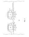
- FIGS. 7 through 9 Another embodiment of the present invention related to STI is schematically illustrated in FIGS. 7 through 9 , wherein similar features bear similar reference characters.
- a shallow trench 210 is formed in semiconductor substrate 200 .
- a thermal oxide liner 220 is formed in the trench in a conventional manner.
- a first layer of dielectric material 230 is deposited followed by post deposition curing.
- each layer of dielectric material can be deposited at a thickness of about 10 ⁇ to about 500 ⁇ , e.g., about 250 ⁇ about 500 ⁇ .
- Post deposition curing of deposited layer 230 can be implemented, as by heating at a temperature of about 400° C. to about 1000° C.
- a second dielectric layer 240 is deposited followed by post deposition curing. Deposited layer 240 can be cured in the same manner as layer 230 . Subsequently, CMP is implemented resulting in this structure illustrated in FIG. 9 .
- FIGS. 10 through 12 Another embodiment of the present invention related to STI is illustrated in FIGS. 10 through 12 wherein similar features bear similar references characters.
- a shallow trench 210 is formed in semiconductor substrate 200 and a thermal oxide liner 220 formed therein.
- a first dielectric layer 250 is deposited followed by post deposition curing to obtain uniform properties and ensure a uniformly high etch rate throughout the thickness of layer 250 .
- second dielectric layer 260 is deposited followed by post deposition curing for homogenization.
- a third dielectric layer 270 is then deposited followed by post deposition curing for homogeneity. Subsequently, as illustrated in FIG. 12 , CMP is implemented to form the completed STI structure.
- the present invention is applicable in various of stages of semiconductor fabrication wherein a dielectric layer is deposited within an opening or a gap.
- Embodiments of the present invention ensure that gap-filling is implemented without generating voids and to ensure that uniform properties are obtained throughout the entire thickness of the dielectric layer, particularly a uniform high etch rate.
- the present invention provides methodology enabling the fabrication of semiconductor devices, particularly flash memory devices, such as mirrorbit devices, exhibiting improved reliability with homogeneous gap-filling.
- semiconductor devices particularly flash memory devices, such as mirrorbit devices, exhibiting improved reliability with homogeneous gap-filling.
- Semiconductor memory devices produced in accordance with the present invention enjoy industrial applicability in various commercial electronic devices, such as computers, mobile phones, cellular handsets, smartphones, set-top boxes, DVD players and recorders, automotive navigation, printers and peripherals, networking and telecom equipment, gaming systems, and digital cameras.
Abstract
Description
Claims (14)
Priority Applications (1)
| Application Number | Priority Date | Filing Date | Title |
|---|---|---|---|
| US12/982,364 US8415256B1 (en) | 2006-04-21 | 2010-12-30 | Gap-filling with uniform properties |
Applications Claiming Priority (2)
| Application Number | Priority Date | Filing Date | Title |
|---|---|---|---|
| US11/408,086 US7884030B1 (en) | 2006-04-21 | 2006-04-21 | Gap-filling with uniform properties |
| US12/982,364 US8415256B1 (en) | 2006-04-21 | 2010-12-30 | Gap-filling with uniform properties |
Related Parent Applications (1)
| Application Number | Title | Priority Date | Filing Date |
|---|---|---|---|
| US11/408,086 Continuation US7884030B1 (en) | 2006-04-21 | 2006-04-21 | Gap-filling with uniform properties |
Publications (1)
| Publication Number | Publication Date |
|---|---|
| US8415256B1 true US8415256B1 (en) | 2013-04-09 |
Family
ID=43531939
Family Applications (2)
| Application Number | Title | Priority Date | Filing Date |
|---|---|---|---|
| US11/408,086 Active 2027-04-07 US7884030B1 (en) | 2006-04-21 | 2006-04-21 | Gap-filling with uniform properties |
| US12/982,364 Active US8415256B1 (en) | 2006-04-21 | 2010-12-30 | Gap-filling with uniform properties |
Family Applications Before (1)
| Application Number | Title | Priority Date | Filing Date |
|---|---|---|---|
| US11/408,086 Active 2027-04-07 US7884030B1 (en) | 2006-04-21 | 2006-04-21 | Gap-filling with uniform properties |
Country Status (1)
| Country | Link |
|---|---|
| US (2) | US7884030B1 (en) |
Cited By (4)
| Publication number | Priority date | Publication date | Assignee | Title |
|---|---|---|---|---|
| US20140191358A1 (en) * | 2013-01-08 | 2014-07-10 | United Microelectronics Corp. | Two-Portion Shallow-Trench Isolation |
| US20150140780A1 (en) * | 2013-11-21 | 2015-05-21 | United Microelectronics Corp. | Method for fabricating shallow trench isolation structure |
| US9379194B2 (en) | 2014-11-09 | 2016-06-28 | Tower Semiconductor Ltd. | Floating gate NVM with low-moisture-content oxide cap layer |
| US9431455B2 (en) | 2014-11-09 | 2016-08-30 | Tower Semiconductor, Ltd. | Back-end processing using low-moisture content oxide cap layer |
Families Citing this family (4)
| Publication number | Priority date | Publication date | Assignee | Title |
|---|---|---|---|---|
| US7884030B1 (en) * | 2006-04-21 | 2011-02-08 | Advanced Micro Devices, Inc. and Spansion LLC | Gap-filling with uniform properties |
| TWI579959B (en) * | 2013-01-07 | 2017-04-21 | 聯華電子股份有限公司 | Shallow trench isolation and method of forming the same |
| US9673194B2 (en) * | 2013-10-31 | 2017-06-06 | Taiwan Semiconductor Manufacturing Company Limited | Semiconductor arrangement and formation thereof |
| GB2577112A (en) * | 2018-09-14 | 2020-03-18 | Flexenable Ltd | Forming dielectric for electronic devices |
Citations (38)
| Publication number | Priority date | Publication date | Assignee | Title |
|---|---|---|---|---|
| US5139971A (en) | 1991-06-07 | 1992-08-18 | Intel Corporation | Anneal to decrease moisture absorbance of intermetal dielectrics |
| US5656861A (en) | 1990-01-12 | 1997-08-12 | Paradigm Technology, Inc. | Self-aligning contact and interconnect structure |
| US5716891A (en) | 1994-06-30 | 1998-02-10 | Nec Corporation | Fabrication process of semiconductor device |
| US5770469A (en) | 1995-12-29 | 1998-06-23 | Lam Research Corporation | Method for forming semiconductor structure using modulation doped silicate glasses |
| US5858876A (en) | 1996-04-01 | 1999-01-12 | Chartered Semiconductor Manufacturing, Ltd. | Simultaneous deposit and etch method for forming a void-free and gap-filling insulator layer upon a patterned substrate layer |
| US5908308A (en) | 1997-11-26 | 1999-06-01 | Advanced Micro Devices, Inc. | Use of borophosphorous tetraethyl orthosilicate (BPTEOS) to improve isolation in a transistor array |
| US5994231A (en) | 1996-12-24 | 1999-11-30 | Sgs-Thomson Microelectronics S.R.L. | Process for depositing a stratified dielectric structure for enhancing the planarity of semiconductor electronic devices |
| US6048475A (en) | 1997-09-30 | 2000-04-11 | Siemens Aktiengesellschaft | Gapfill of semiconductor structure using doped silicate glasses |
| US6140174A (en) | 1998-09-22 | 2000-10-31 | Samsung Electronics Co., Ltd. | Methods of forming wiring layers on integrated circuits including regions of high and low topography |
| US6150238A (en) * | 1999-03-04 | 2000-11-21 | Mosel Vitelic, Inc. | Method for fabricating a trench isolation |
| US6204125B1 (en) | 1999-06-28 | 2001-03-20 | Hyundai Electronics Industries Co., Ltd. | Method of forming a gate in a stack gate flash EEPROM cell |
| US6232235B1 (en) | 1998-06-03 | 2001-05-15 | Motorola, Inc. | Method of forming a semiconductor device |
| US6265281B1 (en) * | 1997-08-18 | 2001-07-24 | Micron Technology, Inc. | Method for forming dielectric within a recess |
| US6319848B1 (en) | 1993-10-12 | 2001-11-20 | Texas Instruments Incorporated | Inhomogenous composite doped film for low temperature reflow |
| US20010050397A1 (en) | 2000-06-08 | 2001-12-13 | Takuji Matsumoto | Semiconductor device and method of manufacturing the same |
| US6362508B1 (en) | 2000-04-03 | 2002-03-26 | Tower Semiconductor Ltd. | Triple layer pre-metal dielectric structure for CMOS memory devices |
| US20020042186A1 (en) | 1999-03-17 | 2002-04-11 | Markus Kirchhoff | Method of filling gaps on a semiconductor wafer |
| US6376303B1 (en) | 1999-08-25 | 2002-04-23 | Samsung Electronics Co., Ltd. | Method of manufacturing a capacitor having oxide layers with different impurities and method of fabricating a semiconductor device comprising the same |
| US20020052119A1 (en) | 1999-03-31 | 2002-05-02 | Patrick A. Van Cleemput | In-situ flowing bpsg gap fill process using hdp |
| US20020115302A1 (en) | 2001-02-19 | 2002-08-22 | Mukai Kevin M. | Aggregate dielectric layer to reduce nitride consumption |
| US6472750B1 (en) | 1996-12-24 | 2002-10-29 | Stmicroelectronics S.R.L. | Process for realizing an intermediate dielectric layer for enhancing the planarity in semiconductor electronic devices |
| US20020173169A1 (en) | 2001-04-10 | 2002-11-21 | Applied Materials, Inc. | Two-step flourinated-borophosophosilicate glass deposition process |
| US6489253B1 (en) | 2001-02-16 | 2002-12-03 | Advanced Micro Devices, Inc. | Method of forming a void-free interlayer dielectric (ILD0) for 0.18-μm flash memory technology and semiconductor device thereby formed |
| US20030036230A1 (en) | 2000-12-07 | 2003-02-20 | Mehta Sunil D. | Combination of bpteos oxide film with cmp and rta to achieve good data retention |
| US20030086679A1 (en) | 2001-11-07 | 2003-05-08 | Photon-X, Inc. | Polymer optical waveguides on polymer substrates |
| US6613657B1 (en) | 2002-08-30 | 2003-09-02 | Advanced Micro Devices, Inc. | BPSG, SA-CVD liner/P-HDP gap fill |
| US6809402B1 (en) | 2002-08-14 | 2004-10-26 | Advanced Micro Devices, Inc. | Reflowable-doped HDP film |
| US20050200026A1 (en) | 2004-03-10 | 2005-09-15 | Taiwan Semiconductor Manufacturing Co. Ltd. | Contact structure for nanometer characteristic dimensions |
| US6955997B1 (en) | 2003-05-16 | 2005-10-18 | Advanced Micro Devices, Inc. | Laser thermal annealing method for forming semiconductor low-k dielectric layer |
| US20050266676A1 (en) | 1998-08-27 | 2005-12-01 | Micron Technology, Inc. | Multi-layer dielectric and method of forming same |
| US20060030165A1 (en) | 2004-08-04 | 2006-02-09 | Applied Materials, Inc. A Delaware Corporation | Multi-step anneal of thin films for film densification and improved gap-fill |
| US20060205112A1 (en) | 2005-03-04 | 2006-09-14 | Martin Standing | Semiconductor package fabrication |
| US7118987B2 (en) | 2004-01-29 | 2006-10-10 | Taiwan Semiconductor Manufacturing Co., Ltd. | Method of achieving improved STI gap fill with reduced stress |
| US20070072387A1 (en) * | 2005-09-28 | 2007-03-29 | Su-Chen Lai | Method of fabricating shallow trench isolation structure |
| US20080138983A1 (en) | 2006-12-06 | 2008-06-12 | Taiwan Semiconductor Manufacturing Co., Ltd. | Method of forming tensile stress films for NFET performance enhancement |
| US20080280441A1 (en) | 2007-05-11 | 2008-11-13 | Hynix Semiconductor Inc. | Method of Forming Isolation Layer of Flash Memory Device |
| US7884030B1 (en) * | 2006-04-21 | 2011-02-08 | Advanced Micro Devices, Inc. and Spansion LLC | Gap-filling with uniform properties |
| US8026151B2 (en) * | 2006-05-26 | 2011-09-27 | Semiconductor Manufacturing International (Shanghai) Corporation | Method with high gapfill capability for semiconductor devices |
Family Cites Families (1)
| Publication number | Priority date | Publication date | Assignee | Title |
|---|---|---|---|---|
| US6649514B1 (en) * | 2002-09-06 | 2003-11-18 | Lattice Semiconductor Corporation | EEPROM device having improved data retention and process for fabricating the device |
-
2006
- 2006-04-21 US US11/408,086 patent/US7884030B1/en active Active
-
2010
- 2010-12-30 US US12/982,364 patent/US8415256B1/en active Active
Patent Citations (39)
| Publication number | Priority date | Publication date | Assignee | Title |
|---|---|---|---|---|
| US5656861A (en) | 1990-01-12 | 1997-08-12 | Paradigm Technology, Inc. | Self-aligning contact and interconnect structure |
| US5139971A (en) | 1991-06-07 | 1992-08-18 | Intel Corporation | Anneal to decrease moisture absorbance of intermetal dielectrics |
| US6319848B1 (en) | 1993-10-12 | 2001-11-20 | Texas Instruments Incorporated | Inhomogenous composite doped film for low temperature reflow |
| US5716891A (en) | 1994-06-30 | 1998-02-10 | Nec Corporation | Fabrication process of semiconductor device |
| US5770469A (en) | 1995-12-29 | 1998-06-23 | Lam Research Corporation | Method for forming semiconductor structure using modulation doped silicate glasses |
| US5858876A (en) | 1996-04-01 | 1999-01-12 | Chartered Semiconductor Manufacturing, Ltd. | Simultaneous deposit and etch method for forming a void-free and gap-filling insulator layer upon a patterned substrate layer |
| US5994231A (en) | 1996-12-24 | 1999-11-30 | Sgs-Thomson Microelectronics S.R.L. | Process for depositing a stratified dielectric structure for enhancing the planarity of semiconductor electronic devices |
| US6472750B1 (en) | 1996-12-24 | 2002-10-29 | Stmicroelectronics S.R.L. | Process for realizing an intermediate dielectric layer for enhancing the planarity in semiconductor electronic devices |
| US6265281B1 (en) * | 1997-08-18 | 2001-07-24 | Micron Technology, Inc. | Method for forming dielectric within a recess |
| US6096654A (en) | 1997-09-30 | 2000-08-01 | Siemens Aktiengesellschaft | Gapfill of semiconductor structure using doped silicate glasses |
| US6048475A (en) | 1997-09-30 | 2000-04-11 | Siemens Aktiengesellschaft | Gapfill of semiconductor structure using doped silicate glasses |
| US5908308A (en) | 1997-11-26 | 1999-06-01 | Advanced Micro Devices, Inc. | Use of borophosphorous tetraethyl orthosilicate (BPTEOS) to improve isolation in a transistor array |
| US6232235B1 (en) | 1998-06-03 | 2001-05-15 | Motorola, Inc. | Method of forming a semiconductor device |
| US20050266676A1 (en) | 1998-08-27 | 2005-12-01 | Micron Technology, Inc. | Multi-layer dielectric and method of forming same |
| US6140174A (en) | 1998-09-22 | 2000-10-31 | Samsung Electronics Co., Ltd. | Methods of forming wiring layers on integrated circuits including regions of high and low topography |
| US6150238A (en) * | 1999-03-04 | 2000-11-21 | Mosel Vitelic, Inc. | Method for fabricating a trench isolation |
| US20020042186A1 (en) | 1999-03-17 | 2002-04-11 | Markus Kirchhoff | Method of filling gaps on a semiconductor wafer |
| US20020052119A1 (en) | 1999-03-31 | 2002-05-02 | Patrick A. Van Cleemput | In-situ flowing bpsg gap fill process using hdp |
| US6204125B1 (en) | 1999-06-28 | 2001-03-20 | Hyundai Electronics Industries Co., Ltd. | Method of forming a gate in a stack gate flash EEPROM cell |
| US6376303B1 (en) | 1999-08-25 | 2002-04-23 | Samsung Electronics Co., Ltd. | Method of manufacturing a capacitor having oxide layers with different impurities and method of fabricating a semiconductor device comprising the same |
| US6362508B1 (en) | 2000-04-03 | 2002-03-26 | Tower Semiconductor Ltd. | Triple layer pre-metal dielectric structure for CMOS memory devices |
| US20010050397A1 (en) | 2000-06-08 | 2001-12-13 | Takuji Matsumoto | Semiconductor device and method of manufacturing the same |
| US20030036230A1 (en) | 2000-12-07 | 2003-02-20 | Mehta Sunil D. | Combination of bpteos oxide film with cmp and rta to achieve good data retention |
| US6489253B1 (en) | 2001-02-16 | 2002-12-03 | Advanced Micro Devices, Inc. | Method of forming a void-free interlayer dielectric (ILD0) for 0.18-μm flash memory technology and semiconductor device thereby formed |
| US20020115302A1 (en) | 2001-02-19 | 2002-08-22 | Mukai Kevin M. | Aggregate dielectric layer to reduce nitride consumption |
| US20020173169A1 (en) | 2001-04-10 | 2002-11-21 | Applied Materials, Inc. | Two-step flourinated-borophosophosilicate glass deposition process |
| US20030086679A1 (en) | 2001-11-07 | 2003-05-08 | Photon-X, Inc. | Polymer optical waveguides on polymer substrates |
| US6809402B1 (en) | 2002-08-14 | 2004-10-26 | Advanced Micro Devices, Inc. | Reflowable-doped HDP film |
| US6613657B1 (en) | 2002-08-30 | 2003-09-02 | Advanced Micro Devices, Inc. | BPSG, SA-CVD liner/P-HDP gap fill |
| US6955997B1 (en) | 2003-05-16 | 2005-10-18 | Advanced Micro Devices, Inc. | Laser thermal annealing method for forming semiconductor low-k dielectric layer |
| US7118987B2 (en) | 2004-01-29 | 2006-10-10 | Taiwan Semiconductor Manufacturing Co., Ltd. | Method of achieving improved STI gap fill with reduced stress |
| US20050200026A1 (en) | 2004-03-10 | 2005-09-15 | Taiwan Semiconductor Manufacturing Co. Ltd. | Contact structure for nanometer characteristic dimensions |
| US20060030165A1 (en) | 2004-08-04 | 2006-02-09 | Applied Materials, Inc. A Delaware Corporation | Multi-step anneal of thin films for film densification and improved gap-fill |
| US20060205112A1 (en) | 2005-03-04 | 2006-09-14 | Martin Standing | Semiconductor package fabrication |
| US20070072387A1 (en) * | 2005-09-28 | 2007-03-29 | Su-Chen Lai | Method of fabricating shallow trench isolation structure |
| US7884030B1 (en) * | 2006-04-21 | 2011-02-08 | Advanced Micro Devices, Inc. and Spansion LLC | Gap-filling with uniform properties |
| US8026151B2 (en) * | 2006-05-26 | 2011-09-27 | Semiconductor Manufacturing International (Shanghai) Corporation | Method with high gapfill capability for semiconductor devices |
| US20080138983A1 (en) | 2006-12-06 | 2008-06-12 | Taiwan Semiconductor Manufacturing Co., Ltd. | Method of forming tensile stress films for NFET performance enhancement |
| US20080280441A1 (en) | 2007-05-11 | 2008-11-13 | Hynix Semiconductor Inc. | Method of Forming Isolation Layer of Flash Memory Device |
Cited By (9)
| Publication number | Priority date | Publication date | Assignee | Title |
|---|---|---|---|---|
| US20140191358A1 (en) * | 2013-01-08 | 2014-07-10 | United Microelectronics Corp. | Two-Portion Shallow-Trench Isolation |
| US8823132B2 (en) * | 2013-01-08 | 2014-09-02 | United Microelectronics Corp. | Two-portion shallow-trench isolation |
| US8912074B2 (en) | 2013-01-08 | 2014-12-16 | United Microelectronics Corp. | Method of forming shallow trench isolations |
| US8928112B2 (en) | 2013-01-08 | 2015-01-06 | United Microelectronics Corp. | Shallow trench isolation |
| US9337260B2 (en) | 2013-01-08 | 2016-05-10 | United Microelectronics Corp. | Shallow trench isolation in bulk substrate |
| US20150140780A1 (en) * | 2013-11-21 | 2015-05-21 | United Microelectronics Corp. | Method for fabricating shallow trench isolation structure |
| US9130014B2 (en) * | 2013-11-21 | 2015-09-08 | United Microelectronics Corp. | Method for fabricating shallow trench isolation structure |
| US9379194B2 (en) | 2014-11-09 | 2016-06-28 | Tower Semiconductor Ltd. | Floating gate NVM with low-moisture-content oxide cap layer |
| US9431455B2 (en) | 2014-11-09 | 2016-08-30 | Tower Semiconductor, Ltd. | Back-end processing using low-moisture content oxide cap layer |
Also Published As
| Publication number | Publication date |
|---|---|
| US7884030B1 (en) | 2011-02-08 |
Similar Documents
| Publication | Publication Date | Title |
|---|---|---|
| US8415256B1 (en) | Gap-filling with uniform properties | |
| US20080096364A1 (en) | Conformal liner for gap-filling | |
| US7564090B2 (en) | Transistor of a semiconductor device | |
| US20040178470A1 (en) | Semiconductor memory device and method of manufacturing the same | |
| KR20100131720A (en) | Method of manufacturing nonvolatile memory device | |
| KR101217260B1 (en) | Method for fabricating a memory cell structure having nitride layer with reduced charge loss | |
| US6969653B2 (en) | Methods of manufacturing and-type flash memory devices | |
| KR100806787B1 (en) | Method of Manufacturing Flash Semiconductor Device | |
| JP4445403B2 (en) | Manufacturing method of semiconductor device | |
| US7829936B2 (en) | Split charge storage node inner spacer process | |
| WO2009136606A1 (en) | Semiconductor device manufacturing method | |
| US9117665B2 (en) | Nonvolatile semiconductor memory device and manufacturing method thereof | |
| US20080160784A1 (en) | Method of manufacturing semiconductor device | |
| US20070275519A1 (en) | Method of manufacturing non-volatile memory device | |
| KR100794085B1 (en) | Method of manufacturing flash memory device | |
| KR100771807B1 (en) | Flash memory device and method for fabricating the same | |
| US7023046B2 (en) | Undoped oxide liner/BPSG for improved data retention | |
| CN108389864B (en) | Method for manufacturing three-dimensional flash memory device | |
| CN1674257A (en) | Fast-flash memory structure and producing method thereof | |
| US7867849B2 (en) | Method of manufacturing a non-volatile semiconductor device | |
| US7038304B2 (en) | Semiconductor memory device and manufacturing method thereof | |
| KR100691946B1 (en) | Method of manufacturing a flash memory device | |
| CN1209811C (en) | Method for reducing random bit failure of flash memory | |
| KR100865037B1 (en) | Method of manufacturing flash memory device | |
| US20040106255A1 (en) | Manufacturing method of flash memory device |
Legal Events
| Date | Code | Title | Description |
|---|---|---|---|
| STCF | Information on status: patent grant |
Free format text: PATENTED CASE |
|
| AS | Assignment |
Owner name: ADVANCED MICRO DEVICES, INC., CALIFORNIA Free format text: ASSIGNMENT OF ASSIGNORS INTEREST;ASSIGNORS:TOKUNO, HIROKAZU;NGO, MINH VAN;PHAM, HIEU;AND OTHERS;SIGNING DATES FROM 20060320 TO 20060322;REEL/FRAME:031354/0670 Owner name: SPANSION LLC, CALIFORNIA Free format text: ASSIGNMENT OF ASSIGNORS INTEREST;ASSIGNORS:TOKUNO, HIROKAZU;NGO, MINH VAN;PHAM, HIEU;AND OTHERS;SIGNING DATES FROM 20060320 TO 20060322;REEL/FRAME:031354/0670 |
|
| AS | Assignment |
Owner name: MORGAN STANLEY SENIOR FUNDING, INC., NEW YORK Free format text: SECURITY INTEREST;ASSIGNORS:CYPRESS SEMICONDUCTOR CORPORATION;SPANSION LLC;REEL/FRAME:035240/0429 Effective date: 20150312 |
|
| FPAY | Fee payment |
Year of fee payment: 4 |
|
| AS | Assignment |
Owner name: SPANSION LLC, CALIFORNIA Free format text: ASSIGNMENT OF ASSIGNORS INTEREST;ASSIGNOR:ADVANCED MICRO DEVICES, INC.;REEL/FRAME:042416/0448 Effective date: 20170509 |
|
| AS | Assignment |
Owner name: MUFG UNION BANK, N.A., CALIFORNIA Free format text: ASSIGNMENT AND ASSUMPTION OF SECURITY INTEREST IN INTELLECTUAL PROPERTY;ASSIGNOR:MORGAN STANLEY SENIOR FUNDING, INC.;REEL/FRAME:050896/0366 Effective date: 20190731 |
|
| MAFP | Maintenance fee payment |
Free format text: PAYMENT OF MAINTENANCE FEE, 8TH YEAR, LARGE ENTITY (ORIGINAL EVENT CODE: M1552); ENTITY STATUS OF PATENT OWNER: LARGE ENTITY Year of fee payment: 8 |
|
| AS | Assignment |
Owner name: MORGAN STANLEY SENIOR FUNDING, INC., NEW YORK Free format text: CORRECTIVE ASSIGNMENT TO CORRECT THE 8647899 PREVIOUSLY RECORDED ON REEL 035240 FRAME 0429. ASSIGNOR(S) HEREBY CONFIRMS THE SECURITY INTERST;ASSIGNORS:CYPRESS SEMICONDUCTOR CORPORATION;SPANSION LLC;REEL/FRAME:058002/0470 Effective date: 20150312 |
|
| AS | Assignment |
Owner name: SPANSION LLC, CALIFORNIA Free format text: RELEASE BY SECURED PARTY;ASSIGNOR:MUFG UNION BANK, N.A.;REEL/FRAME:059410/0438 Effective date: 20200416 Owner name: CYPRESS SEMICONDUCTOR CORPORATION, CALIFORNIA Free format text: RELEASE BY SECURED PARTY;ASSIGNOR:MUFG UNION BANK, N.A.;REEL/FRAME:059410/0438 Effective date: 20200416 |