US8410427B2 - Semiconductor device, method for manufacturing semiconductor device, apparatus for manufacturing semiconductor device, and method for evaluating semiconductor device - Google Patents
Semiconductor device, method for manufacturing semiconductor device, apparatus for manufacturing semiconductor device, and method for evaluating semiconductor device Download PDFInfo
- Publication number
- US8410427B2 US8410427B2 US13/163,221 US201113163221A US8410427B2 US 8410427 B2 US8410427 B2 US 8410427B2 US 201113163221 A US201113163221 A US 201113163221A US 8410427 B2 US8410427 B2 US 8410427B2
- Authority
- US
- United States
- Prior art keywords
- layer
- semiconductor device
- sputtering
- oxygen
- chamber
- Prior art date
- Legal status (The legal status is an assumption and is not a legal conclusion. Google has not performed a legal analysis and makes no representation as to the accuracy of the status listed.)
- Expired - Fee Related, expires
Links
Images


Classifications
-
- C—CHEMISTRY; METALLURGY
- C23—COATING METALLIC MATERIAL; COATING MATERIAL WITH METALLIC MATERIAL; CHEMICAL SURFACE TREATMENT; DIFFUSION TREATMENT OF METALLIC MATERIAL; COATING BY VACUUM EVAPORATION, BY SPUTTERING, BY ION IMPLANTATION OR BY CHEMICAL VAPOUR DEPOSITION, IN GENERAL; INHIBITING CORROSION OF METALLIC MATERIAL OR INCRUSTATION IN GENERAL
- C23C—COATING METALLIC MATERIAL; COATING MATERIAL WITH METALLIC MATERIAL; SURFACE TREATMENT OF METALLIC MATERIAL BY DIFFUSION INTO THE SURFACE, BY CHEMICAL CONVERSION OR SUBSTITUTION; COATING BY VACUUM EVAPORATION, BY SPUTTERING, BY ION IMPLANTATION OR BY CHEMICAL VAPOUR DEPOSITION, IN GENERAL
- C23C14/00—Coating by vacuum evaporation, by sputtering or by ion implantation of the coating forming material
- C23C14/06—Coating by vacuum evaporation, by sputtering or by ion implantation of the coating forming material characterised by the coating material
- C23C14/14—Metallic material, boron or silicon
- C23C14/16—Metallic material, boron or silicon on metallic substrates or on substrates of boron or silicon
-
- C—CHEMISTRY; METALLURGY
- C23—COATING METALLIC MATERIAL; COATING MATERIAL WITH METALLIC MATERIAL; CHEMICAL SURFACE TREATMENT; DIFFUSION TREATMENT OF METALLIC MATERIAL; COATING BY VACUUM EVAPORATION, BY SPUTTERING, BY ION IMPLANTATION OR BY CHEMICAL VAPOUR DEPOSITION, IN GENERAL; INHIBITING CORROSION OF METALLIC MATERIAL OR INCRUSTATION IN GENERAL
- C23C—COATING METALLIC MATERIAL; COATING MATERIAL WITH METALLIC MATERIAL; SURFACE TREATMENT OF METALLIC MATERIAL BY DIFFUSION INTO THE SURFACE, BY CHEMICAL CONVERSION OR SUBSTITUTION; COATING BY VACUUM EVAPORATION, BY SPUTTERING, BY ION IMPLANTATION OR BY CHEMICAL VAPOUR DEPOSITION, IN GENERAL
- C23C14/00—Coating by vacuum evaporation, by sputtering or by ion implantation of the coating forming material
- C23C14/22—Coating by vacuum evaporation, by sputtering or by ion implantation of the coating forming material characterised by the process of coating
- C23C14/34—Sputtering
-
- H—ELECTRICITY
- H10—SEMICONDUCTOR DEVICES; ELECTRIC SOLID-STATE DEVICES NOT OTHERWISE PROVIDED FOR
- H10W—GENERIC PACKAGES, INTERCONNECTIONS, CONNECTORS OR OTHER CONSTRUCTIONAL DETAILS OF DEVICES COVERED BY CLASS H10
- H10W72/00—Interconnections or connectors in packages
- H10W72/01—Manufacture or treatment
- H10W72/019—Manufacture or treatment of bond pads
- H10W72/01931—Manufacture or treatment of bond pads using blanket deposition
- H10W72/01938—Manufacture or treatment of bond pads using blanket deposition in gaseous form, e.g. by CVD or PVD
-
- H—ELECTRICITY
- H10—SEMICONDUCTOR DEVICES; ELECTRIC SOLID-STATE DEVICES NOT OTHERWISE PROVIDED FOR
- H10W—GENERIC PACKAGES, INTERCONNECTIONS, CONNECTORS OR OTHER CONSTRUCTIONAL DETAILS OF DEVICES COVERED BY CLASS H10
- H10W72/00—Interconnections or connectors in packages
- H10W72/071—Connecting or disconnecting
- H10W72/073—Connecting or disconnecting of die-attach connectors
-
- H—ELECTRICITY
- H10—SEMICONDUCTOR DEVICES; ELECTRIC SOLID-STATE DEVICES NOT OTHERWISE PROVIDED FOR
- H10W—GENERIC PACKAGES, INTERCONNECTIONS, CONNECTORS OR OTHER CONSTRUCTIONAL DETAILS OF DEVICES COVERED BY CLASS H10
- H10W72/00—Interconnections or connectors in packages
- H10W72/071—Connecting or disconnecting
- H10W72/075—Connecting or disconnecting of bond wires
-
- H—ELECTRICITY
- H10—SEMICONDUCTOR DEVICES; ELECTRIC SOLID-STATE DEVICES NOT OTHERWISE PROVIDED FOR
- H10W—GENERIC PACKAGES, INTERCONNECTIONS, CONNECTORS OR OTHER CONSTRUCTIONAL DETAILS OF DEVICES COVERED BY CLASS H10
- H10W72/00—Interconnections or connectors in packages
- H10W72/30—Die-attach connectors
- H10W72/351—Materials of die-attach connectors
- H10W72/352—Materials of die-attach connectors comprising metals or metalloids, e.g. solders
-
- H—ELECTRICITY
- H10—SEMICONDUCTOR DEVICES; ELECTRIC SOLID-STATE DEVICES NOT OTHERWISE PROVIDED FOR
- H10W—GENERIC PACKAGES, INTERCONNECTIONS, CONNECTORS OR OTHER CONSTRUCTIONAL DETAILS OF DEVICES COVERED BY CLASS H10
- H10W72/00—Interconnections or connectors in packages
- H10W72/50—Bond wires
- H10W72/531—Shapes of wire connectors
- H10W72/5363—Shapes of wire connectors the connected ends being wedge-shaped
-
- H—ELECTRICITY
- H10—SEMICONDUCTOR DEVICES; ELECTRIC SOLID-STATE DEVICES NOT OTHERWISE PROVIDED FOR
- H10W—GENERIC PACKAGES, INTERCONNECTIONS, CONNECTORS OR OTHER CONSTRUCTIONAL DETAILS OF DEVICES COVERED BY CLASS H10
- H10W72/00—Interconnections or connectors in packages
- H10W72/50—Bond wires
- H10W72/59—Bond pads specially adapted therefor
-
- H—ELECTRICITY
- H10—SEMICONDUCTOR DEVICES; ELECTRIC SOLID-STATE DEVICES NOT OTHERWISE PROVIDED FOR
- H10W—GENERIC PACKAGES, INTERCONNECTIONS, CONNECTORS OR OTHER CONSTRUCTIONAL DETAILS OF DEVICES COVERED BY CLASS H10
- H10W72/00—Interconnections or connectors in packages
- H10W72/851—Dispositions of multiple connectors or interconnections
- H10W72/874—On different surfaces
- H10W72/884—Die-attach connectors and bond wires
-
- H—ELECTRICITY
- H10—SEMICONDUCTOR DEVICES; ELECTRIC SOLID-STATE DEVICES NOT OTHERWISE PROVIDED FOR
- H10W—GENERIC PACKAGES, INTERCONNECTIONS, CONNECTORS OR OTHER CONSTRUCTIONAL DETAILS OF DEVICES COVERED BY CLASS H10
- H10W72/00—Interconnections or connectors in packages
- H10W72/90—Bond pads, in general
- H10W72/921—Structures or relative sizes of bond pads
- H10W72/923—Bond pads having multiple stacked layers
-
- H—ELECTRICITY
- H10—SEMICONDUCTOR DEVICES; ELECTRIC SOLID-STATE DEVICES NOT OTHERWISE PROVIDED FOR
- H10W—GENERIC PACKAGES, INTERCONNECTIONS, CONNECTORS OR OTHER CONSTRUCTIONAL DETAILS OF DEVICES COVERED BY CLASS H10
- H10W72/00—Interconnections or connectors in packages
- H10W72/90—Bond pads, in general
- H10W72/951—Materials of bond pads
- H10W72/952—Materials of bond pads comprising metals or metalloids, e.g. PbSn, Ag or Cu
-
- H—ELECTRICITY
- H10—SEMICONDUCTOR DEVICES; ELECTRIC SOLID-STATE DEVICES NOT OTHERWISE PROVIDED FOR
- H10W—GENERIC PACKAGES, INTERCONNECTIONS, CONNECTORS OR OTHER CONSTRUCTIONAL DETAILS OF DEVICES COVERED BY CLASS H10
- H10W90/00—Package configurations
- H10W90/701—Package configurations characterised by the relative positions of pads or connectors relative to package parts
- H10W90/731—Package configurations characterised by the relative positions of pads or connectors relative to package parts of die-attach connectors
- H10W90/736—Package configurations characterised by the relative positions of pads or connectors relative to package parts of die-attach connectors between a chip and a stacked lead frame, conducting package substrate or heat sink
-
- H—ELECTRICITY
- H10—SEMICONDUCTOR DEVICES; ELECTRIC SOLID-STATE DEVICES NOT OTHERWISE PROVIDED FOR
- H10W—GENERIC PACKAGES, INTERCONNECTIONS, CONNECTORS OR OTHER CONSTRUCTIONAL DETAILS OF DEVICES COVERED BY CLASS H10
- H10W90/00—Package configurations
- H10W90/701—Package configurations characterised by the relative positions of pads or connectors relative to package parts
- H10W90/751—Package configurations characterised by the relative positions of pads or connectors relative to package parts of bond wires
- H10W90/756—Package configurations characterised by the relative positions of pads or connectors relative to package parts of bond wires between a chip and a stacked lead frame, conducting package substrate or heat sink
Definitions
- the present teachings relate to a semiconductor device, a method and apparatus for manufacturing the semiconductor device, and a method for evaluating the semiconductor device.
- the lower surface electrode is first connected and fixed to an external member such as a lead frame by soldering, and wire bonding is subsequently performed on an upper surface electrode formed on an upper surface of the semiconductor substrate.
- the lower surface electrode is configured such that an aluminum layer, a titanium layer, a nickel layer, and a gold layer are laminated in order from a semiconductor substrate side.
- Characteristics required for the lower surface electrode include superior adhesiveness with the semiconductor substrate or solder and a high adhesion between respective metal layers composing the lower surface electrode. Insufficiency of these characteristics in the lower surface electrode may cause a defect in the wire bonding process. Therefore, for example, Japanese Patent Application Publication No. H10-163467 proposes subjecting a lower surface electrode formed by vapor deposition to heat treatment at 400 to 450° C. in order to improve adhesion between the respective metal layers composing the lower surface electrode.
- the present teachings have been made in consideration of the above, and an object thereof is to suppress the separation (i.e., the occurrence of the defect such as cratering) at an interface between the titanium layer and the nickel layer which compose the lower surface electrode of the semiconductor device.
- the present teachings provide a method for manufacturing a semiconductor device including a semiconductor substrate and a lower surface electrode in which an aluminum layer (including an aluminum containing layer), a titanium layer, a nickel layer, and a nickel oxidation-prevention layer are laminated in order from a semiconductor substrate side, wherein the titanium layer of the lower electrode is formed by sputtering in an atmosphere of a partial pressure of oxygen being equal to or less than 5 ⁇ 10 ⁇ 6 Pa.
- the intensive studies by the present inventor have led to a discovery that, during the sputtering process of the titanium layer, the occurrence of a defect such as the cratering can be suppressed by managing the partial pressure of oxygen.
- the titanium layer is formed by performing sputtering in the atmosphere of the partial pressure of oxygen being equal to or less than 5 ⁇ 10 ⁇ 6 Pa, a the oxygen content of the titanium layer in the vicinity of the interface between the titanium layer and the nickel layer can be sufficiently lowered.
- the adhesion between the titanium layer and the nickel layer is improved and the separation (i.e., the occurrence of a defect such as the cratering) at the interface between the titanium layer and the nickel layer can be reduced.
- efficiency of a manufacturing process can also be improved.
- the nickel layer is preferably also formed by sputtering in the atmosphere of the partial pressure of oxygen being equal to or less than 5 ⁇ 10 ⁇ 6 Pa.
- the oxygen content of the nickel layer in the vicinity of the interface between the titanium layer and the nickel layer can be lowered and adhesion of the interface between the titanium layer and the nickel layer can be further improved.
- the method for manufacturing a semiconductor device can be performed by a manufacturing method including steps of: (1) exchanging a target in a chamber of a sputtering apparatus in which the titanium layer is to be sputtered; (2) adjusting a partial pressure of oxygen in the chamber to be equal to or less than a threshold pressure that is predeterminedly set within a range equal to or less than 5 ⁇ 10 ⁇ 6 Pa after the step (1); and (3) starting sputtering in a case where the partial pressure of oxygen in the chamber has become equal to or less than the threshold pressure.
- the present teachings are alternatively capable of providing an apparatus for performing the method for manufacturing a semiconductor device.
- the apparatus for manufacturing the semiconductor device according to the present teachings include: a sputtering apparatus; a detector that detects a partial pressure of oxygen in a chamber of the sputtering apparatus; an adjustor that adjusts the partial pressure of oxygen in the chamber; and a controller.
- the controller controls the adjustor according to a detected value of the detector so that a titanium layer is formed by sputtering in an atmosphere of the partial pressure of oxygen being equal to or less than 5 ⁇ 10 ⁇ 6 Pa.
- the controller may control the sputtering apparatus to start sputtering in a case where the detected value of the detector is equal to or less than a threshold pressure that is predeterminedly set within a range equal to or less than 5 ⁇ 10 ⁇ 6 Pa.
- the present teachings is alternatively capable of providing a semiconductor device with a low defective rate.
- the intensive studies by the present inventor have led to a discovery that separation at the interface between the titanium layer and the nickel layer can be prevented with a semiconductor device including: a semiconductor substrate; and an lower surface electrode in which an aluminum containing layer, a titanium layer, a nickel layer, and a nickel oxidation-prevention layer are laminated in order from a semiconductor substrate side, wherein an oxygen atom count detected by Secondary Ion Mass Spectrometry in an interface between the titanium layer and the nickel layer is equal to or less than 2 ⁇ 10 4 counts per second.
- the present teachings are alternatively capable of providing a method for evaluating quality of a semiconductor device.
- the semiconductor device is judged as having superior panty in a case where an oxygen atom count detected by Secondary Ion Mass Spectrometry in an interface between the titanium layer and the nickel layer is equal to or less than a threshold number that is predeterminedly set within a range equal to or less than 2 ⁇ 10 4 counts per second. Consequently, defective products in which separation occurs at the interface between the titanium layer and the nickel layer of the lower surface electrode or the like can be eliminated.
- a semiconductor device in which a defect such as cratering is likely to occur can be eliminated prior to performing a soldering process or a wire bonding process.
- the efficiency of the manufacturing process can be improved while suppressing the occurrence of defects in semiconductor devices in which the separation occurs at the interface between the titanium layer and the nickel layer composing the lower surface electrode.
- FIG. 1 is a diagram showing a semiconductor device according to an embodiment.
- FIG. 2A is a diagram showing a state where the semiconductor device according to the embodiment is connected to an external member.
- FIG. 2B is a diagram showing a state where the semiconductor device according to the embodiment is connected to an external member.
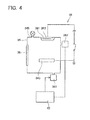
- FIG. 3 is a diagram showing a sputtering apparatus comprising a manufacturing apparatus for manufacturing the semiconductor device according to the embodiment.
- FIG. 4 is a diagram showing the a sputtering apparatus comprising the manufacturing apparatus for manufacturing the semiconductor device according to the embodiment.
- FIG. 5 shows a SIMS analysis result of a lower surface electrode of the semiconductor device according to the embodiment.
- FIG. 6 shows a SIMS analysis result of a lower surface electrode of a semiconductor device according to a comparative example.
- FIG. 7 shows a SIMS analysis result of a lower surface electrode of a conventional semiconductor device.
- FIG. 8 is a SEM image showing a cross section of the lower surface electrode of the conventional semiconductor device.
- FIG. 9 is a SEM image showing a cross section of the lower surface electrode of the conventional semiconductor device.
- a semiconductor device 10 comprises a semiconductor substrate 1 , a lower surface electrode Z and an upper surface electrode 3 .
- an aluminum-silicon alloy (Al—Si) layer 4 as an aluminum containing layer
- a titanium (Ti) layer 5 a nickel (Ni) layer 6
- a gold (Au) layer 7 as a nickel oxidation-prevention layer are laminated in this order from a side of the semiconductor substrate 1 .
- Al alloy may be used as in the present embodiment or high purity Al may alternatively be used.
- a semiconductor substrate comprising circuitry formed on a silicon substrate, a silicon carbide substrate, or the like may be used as the semiconductor substrate 1 .
- the Al—Si layer has a thickness of 800 nm
- the Ti layer has a thickness of 200 nm
- the Ni layer 6 has a thickness of 700 nm
- the Au layer 7 has a thickness of 100 nm.
- the semiconductor device 10 is connected and fixed to an external member 12 such as a lead frame by soldering the lower surface electrode 2 of the semiconductor device 10 .
- a thickness from an upper surface of the upper surface electrode to a lower surface of a solder layer 8 is approximately 165 ⁇ m, and a thickness of the solder layer 8 is approximately 100 ⁇ m.
- the solder layer 8 is made of a tin (Sn) alloy.
- a method for manufacturing the lower surface electrode 2 of the semiconductor device 10 according to the present embodiment will be described. After forming the upper surface electrode 3 on an upper surface of a wafer in which a semiconductor element is formed, the Al—Si layer 4 , the Ti layer 5 , the Ni layer 6 , and the Au layer 7 are formed by sputtering in this order on a lower surface of the wafer to form the lower surface electrode 2 .
- FIGS. 3 and 4 are schematic diagrams showing a configuration of a sputtering apparatus 30 that is used to form the lower surface electrode 2 according to the present embodiment.
- the sputtering apparatus 30 comprises a load lock chamber 32 separated by an openable and closeable door valve 38 , a conveying chamber 33 , a plurality of sputtering chambers 34 , a conveying mechanism (not shown), and a controller 40 .
- Decompression ports (not shown) connected to a decompressor (denoted by reference numeral 341 in FIG. 4 ) are respectively installed in the load lock chamber 32 , the conveying chamber 33 , and the plurality of sputtering chambers 34 .
- a vacuum pump such as a dry pump, a turbo-molecular pump, and a cryopump can be suitably used as the decompressor.
- the decompressor may be installed in each chamber or may be shared by a plurality of chambers.
- the conveying chamber 33 is installed in order to enable the wafer to be transferred in a vacuum between different chambers.
- the load lock chamber 32 and the plurality of sputtering chambers 34 are connected to each other via the conveying chamber 33 .
- a frog-legged robot that holds a side surface of the wafer can be used.
- the conveying mechanism holds one wafer at a time to convey the wafer through the load lock chamber 32 , the conveying chamber 33 , and the sputtering chambers 34 .
- the load lock chamber 32 comprises a wafer inlet (not shown) and a wafer outlet (not shown).
- the wafer is conveyed to the load lock chamber 32 in a state where, for example, a plurality of wafers is mounted on a magazine set.
- the conveying mechanism retrieves one wafer at a time from the magazine set and conveys the wafer through the load lock chamber 32 , the conveying chamber 33 , and the sputtering chambers 34 .
- the plurality of sputtering chambers 34 respectively comprises a deposition device 36 , a gas supply channel 345 , and a detector 347 that detects a partial pressure of oxygen.
- a stage 343 is provided in the sputtering chambers 34 .
- a dielectric layer is provided on the stage 343 .
- the stage 343 applies a voltage between the stage 343 and the wafer, and suctions and holds the wafer using a force generated between the stage 343 and the wafer (a so-called electrostatic chuck).
- the stage 343 comprises a heating unit (not shown) for heating the wafer and a cooling unit (not shown).
- a vacuum pump may be used as the decompressor 341 .
- the decompressor 341 is electrically connected to the controller 40 . Operation of the decompressor 341 is controlled by the controller 40 .
- the detector 347 for example, a quadrupolar gas analyzer capable of measuring a type and a partial pressure of a residual gas in the vacuum can be used.
- the detector 347 is electrically connected to the controller 40 .
- a detection result (a gas type and a partial pressure per type) by the detector 347 is output to the controller 40 .
- Ar gas can be introduced into the sputtering chambers 34 by the gas supply channel 345 .
- the deposition device 36 comprises a backing plate 361 and a target 362 .
- a face of the backing plate 361 on a side opposite to a face on which the target 362 is mounted is cooled by cooling water (not shown).
- the deposition device 36 is configured so as to be capable of applying a high voltage between the target 362 and the wafer mounted on the stage 343 .
- the target 362 and the stage 343 are arranged opposing and separated from each other in the sputtering chambers 34 .
- the target 362 is exchanged in accordance with an electrode layer to be formed.
- a target 362 made of a different metal is provided in each of the plurality of sputtering chambers 34 .
- the Al—Si layer 4 , the Ti layer 5 , the Ni layer 6 , and the Au layer 7 are formed on the lower surface of the wafer.
- a sputtering chamber for forming the Al—Si layer 4 and the Ti layer 5 a sputtering chamber for forming the Ni layer 6 , and a sputtering chamber for forming the Au layer 7 are installed.
- a magazine set on which the wafer is mounted is conveyed to the load lock chamber 32 in a state where the door valve 38 is closed.
- the controller 40 closes the load lock chamber 32 and activates the decompressor, and opens the decompression port installed in the load lock chamber 32 to decompress the load lock chamber 32 .
- the controller 40 opens the door valve 38 separating the load lock chamber 32 from the conveying chamber 33 , then causes the wafer mounted on the magazine set to be moved by the conveying mechanism from the load lock chamber 32 to the conveying chamber 33 , and closes the aforementioned door valve 38 separating the load lock chamber 32 from the conveying chamber 33 .
- the controller 40 opens another door valve 38 separating the conveying chamber 33 from the sputtering chamber 34 , and causes the wafer to be moved by the conveying mechanism to the stage 343 of the sputtering chamber 34 .
- the insides of the conveying chamber 33 and the sputtering chamber 34 have already been decompressed by the decompressor 341 .
- the conveying mechanism mounts the wafer onto the stage 343 of the sputtering chamber 34 so that the lower surface of the wafer faces the target 362 . Subsequently, the controller 40 closes the door valve 38 separating the conveying chamber 33 from the sputtering chamber 34 .
- the controller 40 opens the door valve 38 separating the conveying chamber 33 from the sputtering chamber 34 , causes the wafer to be moved to the next sputtering chamber 34 by the conveying mechanism, and forms another metal layer in the same manner.
- metal layers are laminated on the lower surface of the wafer in an order of the Al—Si layer 4 , the Ti layer 5 , the Ni layer 6 , and the Au layer 7 , and the lower surface electrode 2 is formed on the lower surface of the wafer.
- preprocessing in which several surplus wafers are processed is performed after replacing the target 362 or before manufacturing products.
- the products are manufactured after such preprocessing.
- the sputtering is performed on the wafer to manufacture the products after having decompressed the sputtering chamber 34 .
- the Al—Si layer 4 is formed.
- a target made of an Al—Si alloy is used as the target 362 .
- the wafer is conveyed to the sputtering chamber 34 in which the preprocessing has been completed, and the wafer is installed in a position opposing the target 362 .
- the controller 40 controls the decompressor 341 according to a decompression operational condition that is predeterminedly set to specifically decompress the sputtering chamber 34 , and heats the stage 343 to 70° C.
- introduction of Ar gas from the gas supply channel 345 is started and the deposition device 36 is operated according to an input voltage and a sputtering time indicated in Table 1.
- the Al—Si layer 4 is formed on the lower surface of the wafer by operating the deposition device 36 according to the input power and the sputtering time corresponding to the Al—Si layer indicated in Table 1.
- the controller 40 controls the decompressor 341 according to a decompression operational condition that is predeterminedly set to specifically decompress the sputtering chamber 34 , and heats the stage 343 to 70° C.
- the decompression condition can be determined by performing an experiment in advance. For example, the decompression condition is set in which the sputtering can be performed in an atmosphere of a partial pressure of oxygen being equal to or less than 5 ⁇ 10 ⁇ 6 Pa.
- the controller 40 operates the decompressor 341 according to the decompression condition to create the state where the partial pressure of oxygen in the sputtering chamber 34 is equal to or less than 5 ⁇ 10 ⁇ 6 Pa. Subsequently, the deposition device 36 is operated to start sputtering. Even when the sputtering is in progress, the controller 40 controls the decompressor 341 so that the partial pressure of oxygen in the sputtering chamber 34 is maintained equal to or less than 5 ⁇ 10 ⁇ 6 Pa.
- the Ti layer 5 is formed on the lower surface of the wafer by operating the deposition device 36 according to the input power and the sputtering time corresponding to the Ti layer indicated in Table 1.
- the controller 40 operates the decompressor 341 according to the decompression condition to create the state where the partial pressure of oxygen in the sputtering chamber 34 is equal to or less than 5 ⁇ 10 ⁇ 6 Pa. Subsequently, the deposition device 36 is operated to start sputtering. Even when the sputtering is in progress, the controller 40 controls the decompressor 341 so that the partial pressure of oxygen in the sputtering chamber 34 is maintained equal to or less than 5 ⁇ 10 ⁇ 6 Pa.
- the Ni layer 6 is formed on the lower surface of the wafer by operating the deposition device 36 according to the input power and the sputtering time corresponding to the Ni layer indicated in Table 1.
- the Au layer 7 is formed.
- the wafer is conveyed to the sputtering chamber 34 including the target 362 made of Au.
- the wafer is conveyed to a position that opposes the target 362 .
- the controller 40 controls the decompressor 341 according to a decompression operational condition that is predeterminedly set to specifically decompress the sputtering chamber 34 , and cools the wafer by an electrostatic chuck of the stage 343 .
- the Au layer 7 is formed on the lower surface of the wafer by operating the deposition device 36 .
- the semiconductor device 10 can be manufactured by dicing the wafer after the lower surface electrode 2 is formed on the wafer as described above.
- the controller 40 may alternatively control the decompressor 341 according to a partial pressure of oxygen detected by the detector 347 to start sputtering.
- the controller 40 may control the deposition device 36 to start sputtering according to a threshold A that is predeterminedly set within a range equal to or less than 5 ⁇ 10 ⁇ 6 Pa when the partial pressure of oxygen detected by the detector 347 becomes equal to or less than the threshold A.
- the sputtering can be reliably performed in the atmosphere in which the partial pressure of oxygen is equal to or less than 5 ⁇ 10 ⁇ 6 Pa.
- the partial pressure of oxygen inside the sputtering chamber 34 where the Ti layer formation process was performed was adjusted and the lower surface electrode of the semiconductor device was fabricated.
- a Basic Process Gas Monitor Qulee BGM made by ULVAC, Inc. was used as the detector 347 for detecting the partial pressure of oxygen according to the present embodiment.
- values detected by the detector 347 are shown together with the partial pressure of oxygen inside the sputtering chamber after performing the decompression process.
- the number of samples in which cratering had occurred was studied. The result of the study is also shown in Table 2.
- the preprocessing was performed for 12 hours before forming the Ti layer 5 by sputtering.
- the decompression was performed for six hours using the decompressor 341 provided in the sputtering chamber 34 .
- the partial pressure of oxygen inside the sputtering chamber 34 after performing the decompression process was 5 ⁇ 10 ⁇ 6 Pa.
- the decompression (vacuuming) was performed for nine hours using the decompressor 341 provided in the sputtering chamber 34 .
- the partial pressure of oxygen inside the sputtering chamber 34 after performing the decompression process was 3 ⁇ 10 ⁇ 6 Pa.
- the decompression (vacuuming) was performed for one hour using the decompressor 341 provided in the sputtering chamber 34 .
- the partial pressure of oxygen inside the sputtering chamber 34 after performing the decompression process was 7 ⁇ 10 ⁇ 6 Pa.
- a comparison of the partial pressure of oxygen and a frequency of cratering occurrence in the first and second examples and the comparative example shown in Table 2 reveals that the occurrence of cratering can be effectively suppressed by setting the partial pressure of oxygen inside the sputtering chamber 34 to be equal to or less than 5 ⁇ 10 ⁇ 6 Pa in the process of forming the Ti layer 5 as in the cases of the first and second examples.
- the lower surface electrode of the semiconductor device fabricated according to the second example was analyzed by Secondary Ion Mass Spectrometry (SIMS). A result thereof is shown in FIG. 5 .
- An ADEPT 1010 made by ULVAC-PHI Incorporated was used as an SIMS analyzer and measurement was performed under a condition where Cs+ was used as a primary ion and primary ion acceleration energy was set to 3 keV.
- the SIMS analysis was performed on the lower surface electrode of the semiconductor device fabricated according to the comparative example. A result thereof is shown in FIG. 6 .
- FIGS. 5 and 6 A comparison of FIGS. 5 and 6 reveals that, in FIG. 6 , a sharp peak in oxygen atom counts per second detected by the SIMS analysis exists at an interface between the Ti layer and the Ni layer.
- the oxygen atom count per second detected by the SIMS of the Ti layer at the interface between the Ti layer and the Ni layer is greater than 2 ⁇ 10 4 . This indicates a similar result as the conventional defective sample shown in FIG. 7 .
- the oxygen atom count per second detected by the SIMS analysis does not have a peak at the interface between the Ti layer and the Ni layer.
- the oxygen atom count per second detected by the SIMS of the Ti layer at the interface between the Ti layer and the Ni layer is equal to or smaller than 2 ⁇ 10 4 . From these results, it is revealed that by performing the sputtering process of the Ni layer under the condition where the partial pressure of oxygen is lower than 5 ⁇ 10 ⁇ 6 Pa, the oxygen content can be lowered at the interface between the Ti layer and the Ni layer.
- FIG. 8 shows an SEM photograph of a cross section of a solder layer and a lower surface electrode of a cratering-free sample having superior quality when semiconductor devices fabricated according to the conventional sputtering process are subjected to the soldering process and the wire bonding process.
- FIG. 9 shows an SEM photograph of a cross section of a solder layer and a lower surface electrode of a defective sample in which the cratering has occurred when semiconductor devices fabricated according to the conventional sputtering process are subjected to the soldering process and the wire bonding process. As shown in FIG.
- the lower surface electrode of the defective product in which the cratering has occurred is in a state where the respective metal layers form distinctive layers from the solder layer to the Al—Si layer.
- FIG. 8 showing a state of the lower surface electrode of the cratering-free product having superior quality reveals that the distinctive interface is not formed from the Ti layer to the solder layer and that an alloy is formed by the solder layer, the Ni layer, and the Ti layer.
- FIG. 7 shows an SIMS analysis result of the lower surface electrode of the defective sample described above.
- An ADEPT 1010 made by ULVAC-PHI Incorporated was used as the SIMS analyzer and measurement was performed under a condition where Cs+ was used as a primary ion and primary ion acceleration energy was set to 3 keV.
- Cs+ was used as a primary ion
- primary ion acceleration energy was set to 3 keV.
- FIG. 7 shows a sharp peak in the oxygen atom counts per second detected by the SIMS analysis is observed in the defective sample at the interface between the Ti layer and the Ni layer in the same manner as in FIG. 6 . From the analysis results shown in FIGS. 5 to 9 , it is inferable that alloying of the solder layer, the Ni layer, and the Ti layer cannot be achieved as shown in FIG.
- an oxygen concentration of the Ti layer at the interface between the Ti layer and the Ni layer is too high.
- the oxygen content of the Ti layer can be lowered at the interface between the Ti layer and the Ni layer and the adhesion between the lower surface electrode and the solder layer can be improved.
- the occurrence of separation (cratering) at the interface between the Ti layer and the Ni layer can be suppressed.
- a state where oxygen content does not have a peak at the interface between the Ti layer and the Ni layer can be obtained. Therefore, as shown in FIG. 8 , it is inferable that a state is achieved in which an alloy layer is formed by the solder layer and by the Ti layer and Ni layer of the lower surface electrode and that the occurrence of separation (cratering) at the interface between the Ti layer and the Ni layer is suppressed.
- the oxygen content can be lowered at the interface between the Ti layer and the Ni layer. Therefore, the occurrence of separation (cratering) at the interface of the Ti layer and the Ni layer of the lower surface electrode can be effectively suppressed during the wire bonding process.
- the separation at the interface between the Ti layer and the Ni layer can be prevented when the oxygen atom count detected by Secondary Ion Mass Spectrometry in the Ti layer at the interface between the Ti layer and the Ni layer is equal to or less than 2 ⁇ 10 4 counts per second.
- the Secondary Ion Mass Spectrometry is performed on the lower surface electrode of the semiconductor device provided with the semiconductor substrate and the lower surface electrode in which the Al-containing layer, the Ti layer, the Ni layer, and the Ni oxidation-prevention layer are laminated in order from the semiconductor substrate side.
- the semiconductor device is judged as having superior quality in a case where the oxygen atom count detected by Secondary Ion Mass Spectrometry of the Ti layer at the interface between the Ti layer and the Ni layer is equal to or less than a threshold number that is predeterminedly set within the range equal to or less than 2 ⁇ 10 4 counts per second.
- the defective products in which the separation may occur at the interface between the Ti layer and the Ni layer of the lower surface electrode can be eliminated.
- a semiconductor device in which a defect such as cratering is likely to occur can be eliminated prior to performing the soldering process or the wire bonding process.
- a study of cratering or the like that occurs during the wire bonding process requires soldering and a separation test or the like to be actually performed.
- Implementing a judgment method in which the oxygen content of the interface between the Ti layer and the Ni layer of the lower surface electrode using the SIMS analysis enables the quality of the semiconductor device to be evaluated before performing the soldering and may contribute towards improving the efficiency of the manufacturing process.
Landscapes
- Chemical & Material Sciences (AREA)
- Chemical Kinetics & Catalysis (AREA)
- Engineering & Computer Science (AREA)
- Materials Engineering (AREA)
- Mechanical Engineering (AREA)
- Metallurgy (AREA)
- Organic Chemistry (AREA)
- Electrodes Of Semiconductors (AREA)
- Internal Circuitry In Semiconductor Integrated Circuit Devices (AREA)
Abstract
Description
- 1. A gold (Au) layer is used as a nickel oxidation-prevention layer.
- 2. An aluminum-silicon alloy (Al—Si) is used as an aluminum containing layer.
Embodiments
| TABLE 1 | ||
| Layer to be formed | Input power | Sputtering time |
| Al— |
8 kW | 71 |
| Ti layer | ||
| 3 kW | 68 | |
| Ni layer | ||
| 6 kW | 85 | |
| Au layer | ||
| 1 kW | 25 seconds | |
| TABLE 2 | |||
| Decom- | Partial pressure | Number of cratering | |
| pression | of oxygen | occurrences/Number of | |
| time | [Pa] | manufactured samples | |
| First example | 6 | |
5 × 10⁻⁶ | 0/35 |
| Second example | 9 | |
3 × 10⁻⁶ | 0/35 |
| |
1 | |
7 × 10⁻⁶ | 6/35 |
| example | |||
Claims (3)
Applications Claiming Priority (1)
| Application Number | Priority Date | Filing Date | Title |
|---|---|---|---|
| PCT/JP2009/050578 WO2010082342A1 (en) | 2009-01-16 | 2009-01-16 | Semiconductor device, process for fabricating semiconductor device, apparatus for fabricating semiconductor device, and method for evaluating semiconductor device |
Related Parent Applications (1)
| Application Number | Title | Priority Date | Filing Date |
|---|---|---|---|
| PCT/JP2009/050578 Continuation WO2010082342A1 (en) | 2009-01-16 | 2009-01-16 | Semiconductor device, process for fabricating semiconductor device, apparatus for fabricating semiconductor device, and method for evaluating semiconductor device |
Publications (2)
| Publication Number | Publication Date |
|---|---|
| US20110240846A1 US20110240846A1 (en) | 2011-10-06 |
| US8410427B2 true US8410427B2 (en) | 2013-04-02 |
Family
ID=42339611
Family Applications (1)
| Application Number | Title | Priority Date | Filing Date |
|---|---|---|---|
| US13/163,221 Expired - Fee Related US8410427B2 (en) | 2009-01-16 | 2011-06-17 | Semiconductor device, method for manufacturing semiconductor device, apparatus for manufacturing semiconductor device, and method for evaluating semiconductor device |
Country Status (3)
| Country | Link |
|---|---|
| US (1) | US8410427B2 (en) |
| JP (1) | JP5343979B2 (en) |
| WO (1) | WO2010082342A1 (en) |
Citations (14)
| Publication number | Priority date | Publication date | Assignee | Title |
|---|---|---|---|---|
| JPS58121674A (en) | 1982-01-13 | 1983-07-20 | Nippon Telegr & Teleph Corp <Ntt> | Manufacture of semiconductor device |
| JPH0521382A (en) | 1991-07-10 | 1993-01-29 | Sony Corp | Sputtering device |
| JPH09223779A (en) | 1996-02-16 | 1997-08-26 | Texas Instr Japan Ltd | Ferroelectric capacitor, wiring, semiconductor device and manufacturing method thereof |
| JPH10163467A (en) | 1996-11-27 | 1998-06-19 | Hitachi Ltd | Semiconductor device and electrode forming method |
| JP2000077359A (en) | 1998-09-02 | 2000-03-14 | Matsushita Electronics Industry Corp | Semiconductor device and manufacture thereof |
| US6106676A (en) * | 1998-04-16 | 2000-08-22 | The Boc Group, Inc. | Method and apparatus for reactive sputtering employing two control loops |
| JP2002075872A (en) | 2000-08-24 | 2002-03-15 | Shibaura Mechatronics Corp | Vacuum processing equipment |
| US20020072215A1 (en) * | 2000-12-08 | 2002-06-13 | Nec Corporation | Method for forming barrier layers for solder bumps |
| US20020119657A1 (en) * | 1999-03-09 | 2002-08-29 | Srinivas Gandikota | Method for enhancing the adhesion of copper deposited by chemical vapor deposition |
| US6740577B2 (en) * | 2002-05-21 | 2004-05-25 | St Assembly Test Services Pte Ltd | Method of forming a small pitch torch bump for mounting high-performance flip-flop devices |
| US20040164421A1 (en) * | 2002-05-17 | 2004-08-26 | Tellkamp John P. | Metallic strain-absorbing layer for improved fatigue resistance of solder-attached devices |
| JP2006156910A (en) | 2004-12-01 | 2006-06-15 | Denso Corp | Semiconductor device |
| US20070296080A1 (en) | 2006-06-12 | 2007-12-27 | Toyota Jidosha Kabushiki Kaisha. | Semiconductor devices and method of manufacturing them |
| US7767563B2 (en) * | 2007-03-21 | 2010-08-03 | Intel Corporation | Method of forming a silicide layer on a thinned silicon wafer, and related semiconducting structure |
Family Cites Families (2)
| Publication number | Priority date | Publication date | Assignee | Title |
|---|---|---|---|---|
| JPH04226023A (en) * | 1990-04-16 | 1992-08-14 | Applied Materials Inc | Low nitrogen pressure production for the formation of titanium silicide on semi- conductor wafer |
| JPH0737768A (en) * | 1992-11-26 | 1995-02-07 | Sumitomo Electric Ind Ltd | Method of reinforcing semiconductor wafer and reinforced semiconductor wafer |
-
2009
- 2009-01-16 WO PCT/JP2009/050578 patent/WO2010082342A1/en not_active Ceased
- 2009-01-16 JP JP2010546521A patent/JP5343979B2/en not_active Expired - Fee Related
-
2011
- 2011-06-17 US US13/163,221 patent/US8410427B2/en not_active Expired - Fee Related
Patent Citations (15)
| Publication number | Priority date | Publication date | Assignee | Title |
|---|---|---|---|---|
| JPS58121674A (en) | 1982-01-13 | 1983-07-20 | Nippon Telegr & Teleph Corp <Ntt> | Manufacture of semiconductor device |
| JPH0521382A (en) | 1991-07-10 | 1993-01-29 | Sony Corp | Sputtering device |
| JPH09223779A (en) | 1996-02-16 | 1997-08-26 | Texas Instr Japan Ltd | Ferroelectric capacitor, wiring, semiconductor device and manufacturing method thereof |
| JPH10163467A (en) | 1996-11-27 | 1998-06-19 | Hitachi Ltd | Semiconductor device and electrode forming method |
| US6106676A (en) * | 1998-04-16 | 2000-08-22 | The Boc Group, Inc. | Method and apparatus for reactive sputtering employing two control loops |
| JP2000077359A (en) | 1998-09-02 | 2000-03-14 | Matsushita Electronics Industry Corp | Semiconductor device and manufacture thereof |
| US20020119657A1 (en) * | 1999-03-09 | 2002-08-29 | Srinivas Gandikota | Method for enhancing the adhesion of copper deposited by chemical vapor deposition |
| JP2002075872A (en) | 2000-08-24 | 2002-03-15 | Shibaura Mechatronics Corp | Vacuum processing equipment |
| US20020072215A1 (en) * | 2000-12-08 | 2002-06-13 | Nec Corporation | Method for forming barrier layers for solder bumps |
| US20040164421A1 (en) * | 2002-05-17 | 2004-08-26 | Tellkamp John P. | Metallic strain-absorbing layer for improved fatigue resistance of solder-attached devices |
| US6740577B2 (en) * | 2002-05-21 | 2004-05-25 | St Assembly Test Services Pte Ltd | Method of forming a small pitch torch bump for mounting high-performance flip-flop devices |
| JP2006156910A (en) | 2004-12-01 | 2006-06-15 | Denso Corp | Semiconductor device |
| US20070296080A1 (en) | 2006-06-12 | 2007-12-27 | Toyota Jidosha Kabushiki Kaisha. | Semiconductor devices and method of manufacturing them |
| JP2007335431A (en) | 2006-06-12 | 2007-12-27 | Toyota Motor Corp | Semiconductor device and manufacturing method thereof |
| US7767563B2 (en) * | 2007-03-21 | 2010-08-03 | Intel Corporation | Method of forming a silicide layer on a thinned silicon wafer, and related semiconducting structure |
Also Published As
| Publication number | Publication date |
|---|---|
| WO2010082342A1 (en) | 2010-07-22 |
| JP5343979B2 (en) | 2013-11-13 |
| JPWO2010082342A1 (en) | 2012-06-28 |
| US20110240846A1 (en) | 2011-10-06 |
Similar Documents
| Publication | Publication Date | Title |
|---|---|---|
| US12300658B2 (en) | Copper alloy bonding wire for semiconductor devices | |
| US6562141B2 (en) | Dual degas/cool loadlock cluster tool | |
| US6235656B1 (en) | Dual degas/cool loadlock cluster tool | |
| US20100288730A1 (en) | Vacuum Processing Apparatus And Vacuum Processing Method Using The Same | |
| TW201715066A (en) | Sputtering apparatus and method for determining state thereof | |
| US8410427B2 (en) | Semiconductor device, method for manufacturing semiconductor device, apparatus for manufacturing semiconductor device, and method for evaluating semiconductor device | |
| JP4558431B2 (en) | Cleaning method for semiconductor manufacturing equipment | |
| JP2009191308A (en) | Hard film, hard film forming method, and hard film evaluation method | |
| US9443820B2 (en) | Device and method for bonding substrates | |
| TWI707968B (en) | Method for manufacturing the joint of target and back plate, and the joint of target and back plate | |
| US20220115217A1 (en) | Vacuum processing apparatus | |
| US10790152B2 (en) | Method for etching multilayer film | |
| CN115458394A (en) | Ultrathin wafer ion implantation process | |
| JP2007127032A (en) | Decompression processing device | |
| TWI808439B (en) | Laminated structure and method for manufacturing the laminated structure | |
| CN110534428B (en) | Method for manufacturing metal layer structure, semiconductor device and method for manufacturing semiconductor device | |
| JPH0598434A (en) | Multichamber type sputtering apparatus | |
| KR20250091824A (en) | Preparation method of ta target for semiconductors having reduced oxygen content and the tantalum sputtering target prepared thereby | |
| JP2021512484A (en) | Outgassing effects on process chamber reduction by chamber pumps and purges | |
| CN111771426B (en) | Display device manufacturing method and manufacturing device | |
| Ming et al. | Moisture Effect on Adhesion Between Polybenzoxazole and Sputtering Titanium in WLCSP | |
| CN119943662A (en) | Etching method and wafer for reducing wafer fragmentation rate | |
| JP2011222600A (en) | Method and apparatus for manufacturing semiconductor device | |
| US20240304439A1 (en) | Substrate processing method and substrate processing apparatus | |
| Seryogin et al. | NiV stress control utilizing PVD with an Ar/N2 gas mixture |
Legal Events
| Date | Code | Title | Description |
|---|---|---|---|
| AS | Assignment |
Owner name: TOYOTA JIDOSHA KABUSHIKI KAISHA, JAPAN Free format text: ASSIGNMENT OF ASSIGNORS INTEREST;ASSIGNOR:TAKEUCHI, YASUTAKA;REEL/FRAME:026478/0577 Effective date: 20110517 |
|
| STCF | Information on status: patent grant |
Free format text: PATENTED CASE |
|
| FEPP | Fee payment procedure |
Free format text: PAYOR NUMBER ASSIGNED (ORIGINAL EVENT CODE: ASPN); ENTITY STATUS OF PATENT OWNER: LARGE ENTITY |
|
| FPAY | Fee payment |
Year of fee payment: 4 |
|
| AS | Assignment |
Owner name: DENSO CORPORATION, JAPAN Free format text: ASSIGNMENT OF ASSIGNORS INTEREST;ASSIGNOR:TOYOTA JIDOSHA KABUSHIKI KAISHA;REEL/FRAME:052279/0854 Effective date: 20191229 |
|
| MAFP | Maintenance fee payment |
Free format text: PAYMENT OF MAINTENANCE FEE, 8TH YEAR, LARGE ENTITY (ORIGINAL EVENT CODE: M1552); ENTITY STATUS OF PATENT OWNER: LARGE ENTITY Year of fee payment: 8 |
|
| FEPP | Fee payment procedure |
Free format text: MAINTENANCE FEE REMINDER MAILED (ORIGINAL EVENT CODE: REM.); ENTITY STATUS OF PATENT OWNER: LARGE ENTITY |
|
| LAPS | Lapse for failure to pay maintenance fees |
Free format text: PATENT EXPIRED FOR FAILURE TO PAY MAINTENANCE FEES (ORIGINAL EVENT CODE: EXP.); ENTITY STATUS OF PATENT OWNER: LARGE ENTITY |
|
| STCH | Information on status: patent discontinuation |
Free format text: PATENT EXPIRED DUE TO NONPAYMENT OF MAINTENANCE FEES UNDER 37 CFR 1.362 |
|
| FP | Lapsed due to failure to pay maintenance fee |
Effective date: 20250402 |