US8405138B2 - Densely-packed films of lanthanide oxide nanoparticles via electrophoretic deposition - Google Patents
Densely-packed films of lanthanide oxide nanoparticles via electrophoretic deposition Download PDFInfo
- Publication number
- US8405138B2 US8405138B2 US12/898,159 US89815910A US8405138B2 US 8405138 B2 US8405138 B2 US 8405138B2 US 89815910 A US89815910 A US 89815910A US 8405138 B2 US8405138 B2 US 8405138B2
- Authority
- US
- United States
- Prior art keywords
- film
- nanocrystals
- films
- nanocrystal
- oxide
- Prior art date
- Legal status (The legal status is an assumption and is not a legal conclusion. Google has not performed a legal analysis and makes no representation as to the accuracy of the status listed.)
- Expired - Fee Related, expires
Links
- 239000002105 nanoparticle Substances 0.000 title claims abstract description 73
- 229910000311 lanthanide oxide Inorganic materials 0.000 title claims abstract description 55
- 238000001652 electrophoretic deposition Methods 0.000 title description 75
- 239000000758 substrate Substances 0.000 claims abstract description 77
- 229910001940 europium oxide Inorganic materials 0.000 claims description 69
- AEBZCFFCDTZXHP-UHFFFAOYSA-N europium(3+);oxygen(2-) Chemical compound [O-2].[O-2].[O-2].[Eu+3].[Eu+3] AEBZCFFCDTZXHP-UHFFFAOYSA-N 0.000 claims description 69
- 238000000151 deposition Methods 0.000 claims description 53
- CMIHHWBVHJVIGI-UHFFFAOYSA-N gadolinium(iii) oxide Chemical compound [O-2].[O-2].[O-2].[Gd+3].[Gd+3] CMIHHWBVHJVIGI-UHFFFAOYSA-N 0.000 claims description 42
- 239000003990 capacitor Substances 0.000 claims description 40
- 229910052710 silicon Inorganic materials 0.000 claims description 37
- XUIMIQQOPSSXEZ-UHFFFAOYSA-N Silicon Chemical compound [Si] XUIMIQQOPSSXEZ-UHFFFAOYSA-N 0.000 claims description 35
- 239000010703 silicon Substances 0.000 claims description 35
- 238000012856 packing Methods 0.000 claims description 22
- 239000004065 semiconductor Substances 0.000 claims description 18
- 229910052782 aluminium Inorganic materials 0.000 claims description 13
- XAGFODPZIPBFFR-UHFFFAOYSA-N aluminium Chemical compound [Al] XAGFODPZIPBFFR-UHFFFAOYSA-N 0.000 claims description 12
- 238000003860 storage Methods 0.000 claims description 12
- 238000005566 electron beam evaporation Methods 0.000 claims description 4
- 238000000034 method Methods 0.000 abstract description 43
- 239000002904 solvent Substances 0.000 abstract description 11
- 239000012454 non-polar solvent Substances 0.000 abstract description 9
- 239000010408 film Substances 0.000 description 251
- 239000002159 nanocrystal Substances 0.000 description 212
- 230000008021 deposition Effects 0.000 description 51
- VLKZOEOYAKHREP-UHFFFAOYSA-N n-Hexane Chemical compound CCCCCC VLKZOEOYAKHREP-UHFFFAOYSA-N 0.000 description 48
- 239000000725 suspension Substances 0.000 description 42
- 229910001938 gadolinium oxide Inorganic materials 0.000 description 34
- 239000002245 particle Substances 0.000 description 22
- 229910052737 gold Inorganic materials 0.000 description 21
- 239000010931 gold Substances 0.000 description 21
- PCHJSUWPFVWCPO-UHFFFAOYSA-N gold Chemical group [Au] PCHJSUWPFVWCPO-UHFFFAOYSA-N 0.000 description 20
- ZQPPMHVWECSIRJ-KTKRTIGZSA-N oleic acid Chemical compound CCCCCCCC\C=C/CCCCCCCC(O)=O ZQPPMHVWECSIRJ-KTKRTIGZSA-N 0.000 description 20
- 239000003446 ligand Substances 0.000 description 16
- 238000002149 energy-dispersive X-ray emission spectroscopy Methods 0.000 description 15
- 239000000523 sample Substances 0.000 description 15
- 239000011521 glass Substances 0.000 description 14
- WRIDQFICGBMAFQ-UHFFFAOYSA-N (E)-8-Octadecenoic acid Natural products CCCCCCCCCC=CCCCCCCC(O)=O WRIDQFICGBMAFQ-UHFFFAOYSA-N 0.000 description 12
- LQJBNNIYVWPHFW-UHFFFAOYSA-N 20:1omega9c fatty acid Natural products CCCCCCCCCCC=CCCCCCCCC(O)=O LQJBNNIYVWPHFW-UHFFFAOYSA-N 0.000 description 12
- QSBYPNXLFMSGKH-UHFFFAOYSA-N 9-Heptadecensaeure Natural products CCCCCCCC=CCCCCCCCC(O)=O QSBYPNXLFMSGKH-UHFFFAOYSA-N 0.000 description 12
- 239000005642 Oleic acid Substances 0.000 description 12
- ZQPPMHVWECSIRJ-UHFFFAOYSA-N Oleic acid Natural products CCCCCCCCC=CCCCCCCCC(O)=O ZQPPMHVWECSIRJ-UHFFFAOYSA-N 0.000 description 12
- VYPSYNLAJGMNEJ-UHFFFAOYSA-N Silicium dioxide Chemical compound O=[Si]=O VYPSYNLAJGMNEJ-UHFFFAOYSA-N 0.000 description 12
- 230000006870 function Effects 0.000 description 12
- QXJSBBXBKPUZAA-UHFFFAOYSA-N isooleic acid Natural products CCCCCCCC=CCCCCCCCCC(O)=O QXJSBBXBKPUZAA-UHFFFAOYSA-N 0.000 description 12
- 238000005259 measurement Methods 0.000 description 12
- 239000000203 mixture Substances 0.000 description 12
- 238000010521 absorption reaction Methods 0.000 description 11
- 230000000694 effects Effects 0.000 description 11
- 239000000463 material Substances 0.000 description 11
- 230000008569 process Effects 0.000 description 11
- 238000000089 atomic force micrograph Methods 0.000 description 10
- 230000003247 decreasing effect Effects 0.000 description 10
- 239000000243 solution Substances 0.000 description 10
- 230000005684 electric field Effects 0.000 description 9
- 238000000103 photoluminescence spectrum Methods 0.000 description 9
- 230000007704 transition Effects 0.000 description 9
- LFQSCWFLJHTTHZ-UHFFFAOYSA-N Ethanol Chemical compound CCO LFQSCWFLJHTTHZ-UHFFFAOYSA-N 0.000 description 8
- 238000009825 accumulation Methods 0.000 description 8
- 230000005540 biological transmission Effects 0.000 description 8
- AMGQUBHHOARCQH-UHFFFAOYSA-N indium;oxotin Chemical compound [In].[Sn]=O AMGQUBHHOARCQH-UHFFFAOYSA-N 0.000 description 8
- 238000004519 manufacturing process Methods 0.000 description 8
- 230000003287 optical effect Effects 0.000 description 8
- QVGXLLKOCUKJST-UHFFFAOYSA-N atomic oxygen Chemical compound [O] QVGXLLKOCUKJST-UHFFFAOYSA-N 0.000 description 7
- PJXISJQVUVHSOJ-UHFFFAOYSA-N indium(iii) oxide Chemical compound [O-2].[O-2].[O-2].[In+3].[In+3] PJXISJQVUVHSOJ-UHFFFAOYSA-N 0.000 description 7
- 229910052760 oxygen Inorganic materials 0.000 description 7
- 239000001301 oxygen Substances 0.000 description 7
- 238000011160 research Methods 0.000 description 7
- 238000001228 spectrum Methods 0.000 description 7
- 239000010409 thin film Substances 0.000 description 7
- 229910052693 Europium Inorganic materials 0.000 description 6
- 238000005054 agglomeration Methods 0.000 description 6
- 230000002776 aggregation Effects 0.000 description 6
- 238000004458 analytical method Methods 0.000 description 6
- 230000015572 biosynthetic process Effects 0.000 description 6
- OGPBJKLSAFTDLK-UHFFFAOYSA-N europium atom Chemical compound [Eu] OGPBJKLSAFTDLK-UHFFFAOYSA-N 0.000 description 6
- 239000002086 nanomaterial Substances 0.000 description 6
- 238000000746 purification Methods 0.000 description 6
- XOLBLPGZBRYERU-UHFFFAOYSA-N tin dioxide Chemical compound O=[Sn]=O XOLBLPGZBRYERU-UHFFFAOYSA-N 0.000 description 6
- 238000000862 absorption spectrum Methods 0.000 description 5
- 238000012512 characterization method Methods 0.000 description 5
- 238000000724 energy-dispersive X-ray spectrum Methods 0.000 description 5
- 238000012986 modification Methods 0.000 description 5
- 230000004048 modification Effects 0.000 description 5
- 238000000879 optical micrograph Methods 0.000 description 5
- 238000000628 photoluminescence spectroscopy Methods 0.000 description 5
- 239000000377 silicon dioxide Substances 0.000 description 5
- 239000000126 substance Substances 0.000 description 5
- 238000004627 transmission electron microscopy Methods 0.000 description 5
- 238000003917 TEM image Methods 0.000 description 4
- GWEVSGVZZGPLCZ-UHFFFAOYSA-N Titan oxide Chemical compound O=[Ti]=O GWEVSGVZZGPLCZ-UHFFFAOYSA-N 0.000 description 4
- 238000004847 absorption spectroscopy Methods 0.000 description 4
- 238000005119 centrifugation Methods 0.000 description 4
- 230000007547 defect Effects 0.000 description 4
- 238000000921 elemental analysis Methods 0.000 description 4
- SZVJSHCCFOBDDC-UHFFFAOYSA-N ferrosoferric oxide Chemical compound O=[Fe]O[Fe]O[Fe]=O SZVJSHCCFOBDDC-UHFFFAOYSA-N 0.000 description 4
- 238000003384 imaging method Methods 0.000 description 4
- 150000002500 ions Chemical class 0.000 description 4
- 230000003595 spectral effect Effects 0.000 description 4
- 238000000411 transmission spectrum Methods 0.000 description 4
- OKTJSMMVPCPJKN-UHFFFAOYSA-N Carbon Chemical compound [C] OKTJSMMVPCPJKN-UHFFFAOYSA-N 0.000 description 3
- UHYPYGJEEGLRJD-UHFFFAOYSA-N cadmium(2+);selenium(2-) Chemical compound [Se-2].[Cd+2] UHYPYGJEEGLRJD-UHFFFAOYSA-N 0.000 description 3
- 229910052799 carbon Inorganic materials 0.000 description 3
- 238000013461 design Methods 0.000 description 3
- 239000003989 dielectric material Substances 0.000 description 3
- 238000001035 drying Methods 0.000 description 3
- 238000002524 electron diffraction data Methods 0.000 description 3
- 238000005516 engineering process Methods 0.000 description 3
- 230000001747 exhibiting effect Effects 0.000 description 3
- 239000002798 polar solvent Substances 0.000 description 3
- 238000001878 scanning electron micrograph Methods 0.000 description 3
- 235000012239 silicon dioxide Nutrition 0.000 description 3
- 229910001220 stainless steel Inorganic materials 0.000 description 3
- 239000010935 stainless steel Substances 0.000 description 3
- 230000003746 surface roughness Effects 0.000 description 3
- 238000003786 synthesis reaction Methods 0.000 description 3
- ABEXEQSGABRUHS-UHFFFAOYSA-N 16-methylheptadecyl 16-methylheptadecanoate Chemical class CC(C)CCCCCCCCCCCCCCCOC(=O)CCCCCCCCCCCCCCC(C)C ABEXEQSGABRUHS-UHFFFAOYSA-N 0.000 description 2
- CSCPPACGZOOCGX-UHFFFAOYSA-N Acetone Chemical compound CC(C)=O CSCPPACGZOOCGX-UHFFFAOYSA-N 0.000 description 2
- IJGRMHOSHXDMSA-UHFFFAOYSA-N Atomic nitrogen Chemical compound N#N IJGRMHOSHXDMSA-UHFFFAOYSA-N 0.000 description 2
- OAICVXFJPJFONN-UHFFFAOYSA-N Phosphorus Chemical compound [P] OAICVXFJPJFONN-UHFFFAOYSA-N 0.000 description 2
- 238000000149 argon plasma sintering Methods 0.000 description 2
- 238000005266 casting Methods 0.000 description 2
- 239000000919 ceramic Substances 0.000 description 2
- 230000008859 change Effects 0.000 description 2
- 239000002800 charge carrier Substances 0.000 description 2
- 238000000576 coating method Methods 0.000 description 2
- 229910052681 coesite Inorganic materials 0.000 description 2
- 230000000295 complement effect Effects 0.000 description 2
- 229910052906 cristobalite Inorganic materials 0.000 description 2
- 239000013078 crystal Substances 0.000 description 2
- 230000007423 decrease Effects 0.000 description 2
- 238000002296 dynamic light scattering Methods 0.000 description 2
- 230000005284 excitation Effects 0.000 description 2
- 238000002474 experimental method Methods 0.000 description 2
- 238000000605 extraction Methods 0.000 description 2
- 230000005283 ground state Effects 0.000 description 2
- 238000003780 insertion Methods 0.000 description 2
- 230000037431 insertion Effects 0.000 description 2
- 239000012212 insulator Substances 0.000 description 2
- JEIPFZHSYJVQDO-UHFFFAOYSA-N iron(III) oxide Inorganic materials O=[Fe]O[Fe]=O JEIPFZHSYJVQDO-UHFFFAOYSA-N 0.000 description 2
- 238000004020 luminiscence type Methods 0.000 description 2
- 229910052751 metal Inorganic materials 0.000 description 2
- 239000002184 metal Substances 0.000 description 2
- 238000004452 microanalysis Methods 0.000 description 2
- TVMXDCGIABBOFY-UHFFFAOYSA-N octane Chemical compound CCCCCCCC TVMXDCGIABBOFY-UHFFFAOYSA-N 0.000 description 2
- 229940049964 oleate Drugs 0.000 description 2
- 230000001443 photoexcitation Effects 0.000 description 2
- 238000005424 photoluminescence Methods 0.000 description 2
- 238000001556 precipitation Methods 0.000 description 2
- 238000012545 processing Methods 0.000 description 2
- 239000011541 reaction mixture Substances 0.000 description 2
- 230000002441 reversible effect Effects 0.000 description 2
- 229910052814 silicon oxide Inorganic materials 0.000 description 2
- 238000004611 spectroscopical analysis Methods 0.000 description 2
- 230000006641 stabilisation Effects 0.000 description 2
- 238000011105 stabilization Methods 0.000 description 2
- 229910052682 stishovite Inorganic materials 0.000 description 2
- 238000012876 topography Methods 0.000 description 2
- 238000012546 transfer Methods 0.000 description 2
- 229910052905 tridymite Inorganic materials 0.000 description 2
- XLYOFNOQVPJJNP-UHFFFAOYSA-N water Substances O XLYOFNOQVPJJNP-UHFFFAOYSA-N 0.000 description 2
- YUSCRGFYKCAQHE-HQFNMCNFSA-N (8r,9s,13s,14s,17s)-13-methyl-6,7,8,9,11,12,14,15,16,17-decahydrocyclopenta[a]phenanthrene-3,17-diol;(8r,9s,13s,14s,16r,17r)-13-methyl-6,7,8,9,11,12,14,15,16,17-decahydrocyclopenta[a]phenanthrene-3,16,17-triol Chemical compound OC1=CC=C2[C@H]3CC[C@](C)([C@H](CC4)O)[C@@H]4[C@@H]3CCC2=C1.OC1=CC=C2[C@H]3CC[C@](C)([C@H]([C@H](O)C4)O)[C@@H]4[C@@H]3CCC2=C1 YUSCRGFYKCAQHE-HQFNMCNFSA-N 0.000 description 1
- YHPMRHPLAQSPHJ-UHFFFAOYSA-N 3-chloropyrazine-2-carboxamide Chemical compound NC(=O)C1=NC=CN=C1Cl YHPMRHPLAQSPHJ-UHFFFAOYSA-N 0.000 description 1
- VYZAMTAEIAYCRO-UHFFFAOYSA-N Chromium Chemical compound [Cr] VYZAMTAEIAYCRO-UHFFFAOYSA-N 0.000 description 1
- 229910052688 Gadolinium Inorganic materials 0.000 description 1
- 230000005483 Hooke's law Effects 0.000 description 1
- 238000004566 IR spectroscopy Methods 0.000 description 1
- 229910052581 Si3N4 Inorganic materials 0.000 description 1
- BCKXLBQYZLBQEK-KVVVOXFISA-M Sodium oleate Chemical compound [Na+].CCCCCCCC\C=C/CCCCCCCC([O-])=O BCKXLBQYZLBQEK-KVVVOXFISA-M 0.000 description 1
- 230000009471 action Effects 0.000 description 1
- 238000007605 air drying Methods 0.000 description 1
- PNEYBMLMFCGWSK-UHFFFAOYSA-N aluminium oxide Inorganic materials [O-2].[O-2].[O-2].[Al+3].[Al+3] PNEYBMLMFCGWSK-UHFFFAOYSA-N 0.000 description 1
- 238000013459 approach Methods 0.000 description 1
- 238000004630 atomic force microscopy Methods 0.000 description 1
- 230000004888 barrier function Effects 0.000 description 1
- 230000009286 beneficial effect Effects 0.000 description 1
- 244000309464 bull Species 0.000 description 1
- 238000004364 calculation method Methods 0.000 description 1
- 239000002041 carbon nanotube Substances 0.000 description 1
- 238000000701 chemical imaging Methods 0.000 description 1
- 229910052804 chromium Inorganic materials 0.000 description 1
- 239000011651 chromium Substances 0.000 description 1
- 238000004140 cleaning Methods 0.000 description 1
- 238000001246 colloidal dispersion Methods 0.000 description 1
- 239000000084 colloidal system Substances 0.000 description 1
- 239000002872 contrast media Substances 0.000 description 1
- 229910052593 corundum Inorganic materials 0.000 description 1
- 230000007812 deficiency Effects 0.000 description 1
- 238000000280 densification Methods 0.000 description 1
- 230000001419 dependent effect Effects 0.000 description 1
- 238000003795 desorption Methods 0.000 description 1
- 238000011161 development Methods 0.000 description 1
- 238000005328 electron beam physical vapour deposition Methods 0.000 description 1
- 239000000839 emulsion Substances 0.000 description 1
- STVYPZZQOXPZBX-UHFFFAOYSA-N ethanol;hexane;hydrate Chemical compound O.CCO.CCCCCC STVYPZZQOXPZBX-UHFFFAOYSA-N 0.000 description 1
- 238000001704 evaporation Methods 0.000 description 1
- 230000008020 evaporation Effects 0.000 description 1
- 239000006260 foam Substances 0.000 description 1
- UIWYJDYFSGRHKR-UHFFFAOYSA-N gadolinium atom Chemical compound [Gd] UIWYJDYFSGRHKR-UHFFFAOYSA-N 0.000 description 1
- 238000010438 heat treatment Methods 0.000 description 1
- 230000005661 hydrophobic surface Effects 0.000 description 1
- 229910052588 hydroxylapatite Inorganic materials 0.000 description 1
- 229910003437 indium oxide Inorganic materials 0.000 description 1
- 238000002347 injection Methods 0.000 description 1
- 239000007924 injection Substances 0.000 description 1
- 230000003993 interaction Effects 0.000 description 1
- 238000005342 ion exchange Methods 0.000 description 1
- 238000012417 linear regression Methods 0.000 description 1
- 230000007246 mechanism Effects 0.000 description 1
- 238000000386 microscopy Methods 0.000 description 1
- XTAZYLNFDRKIHJ-UHFFFAOYSA-N n,n-dioctyloctan-1-amine Chemical compound CCCCCCCCN(CCCCCCCC)CCCCCCCC XTAZYLNFDRKIHJ-UHFFFAOYSA-N 0.000 description 1
- 239000002114 nanocomposite Substances 0.000 description 1
- 229910052759 nickel Inorganic materials 0.000 description 1
- 229910052757 nitrogen Inorganic materials 0.000 description 1
- 238000005457 optimization Methods 0.000 description 1
- 230000010355 oscillation Effects 0.000 description 1
- XYJRXVWERLGGKC-UHFFFAOYSA-D pentacalcium;hydroxide;triphosphate Chemical compound [OH-].[Ca+2].[Ca+2].[Ca+2].[Ca+2].[Ca+2].[O-]P([O-])([O-])=O.[O-]P([O-])([O-])=O.[O-]P([O-])([O-])=O XYJRXVWERLGGKC-UHFFFAOYSA-D 0.000 description 1
- 229910052697 platinum Inorganic materials 0.000 description 1
- 239000003495 polar organic solvent Substances 0.000 description 1
- 229920000642 polymer Polymers 0.000 description 1
- 238000001314 profilometry Methods 0.000 description 1
- 230000005855 radiation Effects 0.000 description 1
- 229910052761 rare earth metal Inorganic materials 0.000 description 1
- 150000002910 rare earth metals Chemical class 0.000 description 1
- 230000009467 reduction Effects 0.000 description 1
- 230000008521 reorganization Effects 0.000 description 1
- 230000004044 response Effects 0.000 description 1
- 238000010079 rubber tapping Methods 0.000 description 1
- 238000004626 scanning electron microscopy Methods 0.000 description 1
- 238000001338 self-assembly Methods 0.000 description 1
- HQVNEWCFYHHQES-UHFFFAOYSA-N silicon nitride Chemical compound N12[Si]34N5[Si]62N3[Si]51N64 HQVNEWCFYHHQES-UHFFFAOYSA-N 0.000 description 1
- 239000006104 solid solution Substances 0.000 description 1
- 238000001179 sorption measurement Methods 0.000 description 1
- 238000012306 spectroscopic technique Methods 0.000 description 1
- 238000004528 spin coating Methods 0.000 description 1
- 238000004544 sputter deposition Methods 0.000 description 1
- 239000004094 surface-active agent Substances 0.000 description 1
- 238000002207 thermal evaporation Methods 0.000 description 1
- 238000007736 thin film deposition technique Methods 0.000 description 1
- 238000013169 thromboelastometry Methods 0.000 description 1
- 238000010937 topological data analysis Methods 0.000 description 1
- 230000001052 transient effect Effects 0.000 description 1
- 238000002235 transmission spectroscopy Methods 0.000 description 1
- 238000001429 visible spectrum Methods 0.000 description 1
- 238000004846 x-ray emission Methods 0.000 description 1
- 229910001845 yogo sapphire Inorganic materials 0.000 description 1
- 229920001345 ε-poly-D-lysine Polymers 0.000 description 1
Images


Classifications
-
- C—CHEMISTRY; METALLURGY
- C25—ELECTROLYTIC OR ELECTROPHORETIC PROCESSES; APPARATUS THEREFOR
- C25D—PROCESSES FOR THE ELECTROLYTIC OR ELECTROPHORETIC PRODUCTION OF COATINGS; ELECTROFORMING; APPARATUS THEREFOR
- C25D13/00—Electrophoretic coating characterised by the process
- C25D13/02—Electrophoretic coating characterised by the process with inorganic material
-
- B—PERFORMING OPERATIONS; TRANSPORTING
- B82—NANOTECHNOLOGY
- B82Y—SPECIFIC USES OR APPLICATIONS OF NANOSTRUCTURES; MEASUREMENT OR ANALYSIS OF NANOSTRUCTURES; MANUFACTURE OR TREATMENT OF NANOSTRUCTURES
- B82Y10/00—Nanotechnology for information processing, storage or transmission, e.g. quantum computing or single electron logic
-
- B—PERFORMING OPERATIONS; TRANSPORTING
- B82—NANOTECHNOLOGY
- B82Y—SPECIFIC USES OR APPLICATIONS OF NANOSTRUCTURES; MEASUREMENT OR ANALYSIS OF NANOSTRUCTURES; MANUFACTURE OR TREATMENT OF NANOSTRUCTURES
- B82Y30/00—Nanotechnology for materials or surface science, e.g. nanocomposites
-
- B—PERFORMING OPERATIONS; TRANSPORTING
- B82—NANOTECHNOLOGY
- B82Y—SPECIFIC USES OR APPLICATIONS OF NANOSTRUCTURES; MEASUREMENT OR ANALYSIS OF NANOSTRUCTURES; MANUFACTURE OR TREATMENT OF NANOSTRUCTURES
- B82Y40/00—Manufacture or treatment of nanostructures
-
- H—ELECTRICITY
- H01—ELECTRIC ELEMENTS
- H01L—SEMICONDUCTOR DEVICES NOT COVERED BY CLASS H10
- H01L21/00—Processes or apparatus adapted for the manufacture or treatment of semiconductor or solid state devices or of parts thereof
- H01L21/02—Manufacture or treatment of semiconductor devices or of parts thereof
- H01L21/02104—Forming layers
- H01L21/02107—Forming insulating materials on a substrate
- H01L21/02109—Forming insulating materials on a substrate characterised by the type of layer, e.g. type of material, porous/non-porous, pre-cursors, mixtures or laminates
- H01L21/02112—Forming insulating materials on a substrate characterised by the type of layer, e.g. type of material, porous/non-porous, pre-cursors, mixtures or laminates characterised by the material of the layer
- H01L21/02172—Forming insulating materials on a substrate characterised by the type of layer, e.g. type of material, porous/non-porous, pre-cursors, mixtures or laminates characterised by the material of the layer the material containing at least one metal element, e.g. metal oxides, metal nitrides, metal oxynitrides or metal carbides
- H01L21/02175—Forming insulating materials on a substrate characterised by the type of layer, e.g. type of material, porous/non-porous, pre-cursors, mixtures or laminates characterised by the material of the layer the material containing at least one metal element, e.g. metal oxides, metal nitrides, metal oxynitrides or metal carbides characterised by the metal
- H01L21/02192—Forming insulating materials on a substrate characterised by the type of layer, e.g. type of material, porous/non-porous, pre-cursors, mixtures or laminates characterised by the material of the layer the material containing at least one metal element, e.g. metal oxides, metal nitrides, metal oxynitrides or metal carbides characterised by the metal the material containing at least one rare earth metal element, e.g. oxides of lanthanides, scandium or yttrium
-
- H—ELECTRICITY
- H01—ELECTRIC ELEMENTS
- H01L—SEMICONDUCTOR DEVICES NOT COVERED BY CLASS H10
- H01L21/00—Processes or apparatus adapted for the manufacture or treatment of semiconductor or solid state devices or of parts thereof
- H01L21/02—Manufacture or treatment of semiconductor devices or of parts thereof
- H01L21/02104—Forming layers
- H01L21/02107—Forming insulating materials on a substrate
- H01L21/02225—Forming insulating materials on a substrate characterised by the process for the formation of the insulating layer
- H01L21/0226—Forming insulating materials on a substrate characterised by the process for the formation of the insulating layer formation by a deposition process
-
- H—ELECTRICITY
- H10—SEMICONDUCTOR DEVICES; ELECTRIC SOLID-STATE DEVICES NOT OTHERWISE PROVIDED FOR
- H10D—INORGANIC ELECTRIC SEMICONDUCTOR DEVICES
- H10D1/00—Resistors, capacitors or inductors
- H10D1/01—Manufacture or treatment
- H10D1/045—Manufacture or treatment of capacitors having potential barriers, e.g. varactors
- H10D1/047—Manufacture or treatment of capacitors having potential barriers, e.g. varactors of conductor-insulator-semiconductor capacitors, e.g. trench capacitors
-
- H—ELECTRICITY
- H10—SEMICONDUCTOR DEVICES; ELECTRIC SOLID-STATE DEVICES NOT OTHERWISE PROVIDED FOR
- H10D—INORGANIC ELECTRIC SEMICONDUCTOR DEVICES
- H10D1/00—Resistors, capacitors or inductors
- H10D1/60—Capacitors
- H10D1/62—Capacitors having potential barriers
- H10D1/66—Conductor-insulator-semiconductor capacitors, e.g. MOS capacitors
-
- H—ELECTRICITY
- H10—SEMICONDUCTOR DEVICES; ELECTRIC SOLID-STATE DEVICES NOT OTHERWISE PROVIDED FOR
- H10D—INORGANIC ELECTRIC SEMICONDUCTOR DEVICES
- H10D62/00—Semiconductor bodies, or regions thereof, of devices having potential barriers
- H10D62/10—Shapes, relative sizes or dispositions of the regions of the semiconductor bodies; Shapes of the semiconductor bodies
- H10D62/117—Shapes of semiconductor bodies
- H10D62/118—Nanostructure semiconductor bodies
Definitions
- the present invention relates generally to films of nanoparticles, in particular, to films of lanthanide oxide nanoparticles and methods of forming same.
- the Eu 3+ -doped Gd 2 O 3 in microcrystalline form, has been employed in video displays and tri-color fluorescent lamps as a red phosphor [78].
- nanocrystalline form of Eu 3+ -doped sesquioxides has gained research interest due to their potential use in luminescent biological tags, efficient light emitting devices, and high-resolution displays.
- Gd 2 O 3 has received research attention because of its high- ⁇ dielectric properties.
- Gd 2 O 3 has been proposed as silicon dioxide replacement for gate oxide in ultra-small complementary metal-oxide-semiconductor (CMOS) devices [77]. Most applications of luminescent and dielectric materials require their implementation in thin-film form.
- CMOS complementary metal-oxide-semiconductor
- the present invention relates to a method of forming a film of lanthanide oxide nanoparticles.
- the method includes the steps of: (a) providing a first substrate with a conducting surface and a second substrate that is positioned apart from the first substrate, (b) applying a voltage between the first substrate and the second substrate, (c) immersing the first substrate and the second substrate in a solution that comprises a plurality of lanthanide oxide nanoparticles suspended in a non-polar solvent or apolar solvent for a first duration of time effective to form a film of lanthanide oxide nanoparticles on the conducting surface of the first substrate, and (d) after the immersing step, removing the first substrate from the solution and exposing the first substrate to air while maintaining the applied voltage for a second duration of time to dry the film of lanthanide oxide nanoparticles formed on the conducting surface of the first substrate.
- the first substrate is gold-coated glass, gold-coated silicon, stainless steel (316L), indium-tin-oxide (ITO)-coated glass, or doped silicon.
- the applied voltage, V is in the range of 0 volts ⁇ V ⁇ 1000 volts.
- the non-polar solvent or apolar solvent includes at least one of hexane, octane and mixtures thereof, and each of the first duration of time, T1 and the second duration of time voltage, T2, is in the range of 0 minutes ⁇ T1, T2 ⁇ 30 minutes.
- the first duration of time, T1 and the second duration of time voltage, T2 can be same or different.
- the solution has a concentration ranging from about 1 ⁇ 10 14 nanoparticles per cubic centimeter to about 10 ⁇ 10 15 nanoparticles per cubic centimeter.
- the film of lanthanide oxide nanoparticles formed on the conducting surface of the first substrate has a thickness ranging from about 50 to about 500 nm.
- the film of lanthanide oxide nanoparticles formed on the conducting surface of the first substrate has randomly close-packed lanthanide oxide nanoparticles with a packing density of about 66%.
- the lanthanide oxide nanoparticles are europium oxide (Eu 2 O 3 ) nanoparticles or gadolinium oxide (Gd 2 O 3 ) nanoparticles.
- the lanthanide oxide nanoparticles have a core diameter ranging from about 2 to about 3 nm.
- the lanthanide oxide nanoparticles are surface-passivated with oleic acid.
- the present invention provides an article of manufacture having a film of the lanthanide oxide nanoparticles made by the method set forth immediately above.
- the present invention relates to a metal-oxide-semiconductor (MOS) capacitor.
- the MOS capacitor has: (a) a silicon substrate having a first surface, (b) a film of lanthanide oxide nanoparticles formed on the first surface of the silicon substrate using the method set forth immediately above, and (c) an aluminum film formed on the film of lanthanide oxide nanoparticles, wherein the film of lanthanide oxide nanoparticles comprises randomly close-packed lanthanide oxide nanoparticles with a packing density of about 66%.
- the silicon substrate has p-type silicon.
- the first surface of the silicon substrate is a p ⁇ (100) surface of silicon.
- the MOS capacitor further has a film of silicon oxide disposed between the silicon substrate and the film of lanthanide oxide nanoparticles.
- the lanthanide oxide nanoparticles have europium oxide (Eu 2 O 3 ) nanoparticles or gadolinium oxide (Gd 2 O 3 ) nanoparticles.
- the film of lanthanide oxide nanoparticles has a thickness ranging from about 50 to about 500 nm.
- the aluminum film has a thickness of about 300 nm.
- the aluminum film is formed on the film of lanthanide oxide nanoparticles using electron-beam evaporation.
- FIG. 2 shows: (a) optical micrograph of the Eu 2 O 3 film deposited on a gold substrate, which appears golden in colour because of the background gold substrate and the high transparency of the film; (b) EDS spectrum of the film deposited on a gold substrate, which reveals the presence of europium, oxygen and carbon that originates from the oleic-acid-functionalized Eu 2 O 3 nanocrystals and the gold from the substrate; and (c) PL spectra of the Eu 2 O 3 nanocrystal films deposited on the anode and cathode. The spectra are identical to the spectrum of the Eu 2 O 3 nanocrystals. PL spectra are shifted vertically for clarity.
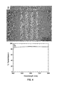
- FIG. 3 shows: (a) SEM image of the nanocrystal film; and (b) AFM image of the nanocrystal film, which reveals deposition of the nanocrystal agglomerates of about 15 nm size. RMS roughness of the film determined from the AFM image is 1.4 nm.
- FIG. 4 shows: (a) optical micrograph of the patterned silicon substrate recorded through the nanocrystal film deposited on ITO-coated glass substrate, which reveals high transparency of the EPD film; and (b) transmission spectrum of a cast film of the Eu 2 O 3 nanocrystals, showing high transparency in the visible region.
- FIG. 5 shows the thickness of the EPD film as a function of the applied voltage for different nanocrystal concentrations. Average film thickness is reported from the thickness measurements at different locations and standard deviation is employed as the error bar. The large error bar indicates decreased film uniformity.
- FIG. 6 shows the electrophoretic mobility measurements of the EPD suspensions with different nanocrystal concentrations.
- FIG. 7 shows AFM images ((a), (b), (c), and (d)) and EDS spectrum ((e), (f), (g), and (h)) of the nanocrystal films deposited with the nanocrystal suspension concentration of 4 ⁇ 10 15 NC cm ⁇ 3 at the applied voltages of 250 V, 500 V, 750 V and 1000 V, respectively.
- the AFM images of the films reveal the agglomerate size of about 130-160 nm and RMS roughness of about 1.6-1.8 nm.
- the morphology and composition of the films were comparable.
- FIG. 8 shows: (a) a schematic of the MOS capacitor structures with NC film as the gate oxide layer according to one embodiment of the present invention; (b) AFM image of the NC film (1 ⁇ m 2 area, height: 20 nm/div) with RMS roughness of about 1.6 nm; inset: TEM image of the about 2.4 nm diameter Gd 2 O 3 nanocrystals (Image: 6 nm ⁇ 6 nm); (c) EDS spectrum of the NC film; and (d) SEM image (top view) of the MOS capacitor structures.
- FIG. 9 shows C-V characteristics of the MOS capacitors, fabricated from NC films that were deposited on the anode and cathode according to one embodiment of the present invention.
- the thickness of the film was 116 nm ⁇ 10 nm, and the average area of the capacitors was 1.96 ⁇ 10 5 ⁇ m 2 .
- FIG. 10 shows C-V characteristics of the MOS capacitors with different thicknesses of the NC films (oxide layer) according to one embodiment of the present invention.
- FIG. 11 shows a graph of capacitance versus inverse of NC film (oxide layer) thickness for four different MOS capacitors according to one embodiment of the present invention.
- FIGS. 1-11 like numbers, if any, indicate like components throughout the views.
- the meaning of “a”, “an”, and “the” includes plural reference unless the context clearly dictates otherwise.
- the meaning of “in” includes “in” and “on” unless the context clearly dictates otherwise.
- titles or subtitles may be used in the specification for the convenience of a reader, which shall have no influence on the scope of the present invention. Additionally, some terms used in this specification are more specifically defined below.
- “around”, “about” or “approximately” shall generally mean within 20 percent, preferably within 10 percent, and more preferably within 5 percent of a given value or range. Numerical quantities given herein are approximate, meaning that the term “around”, “about” or “approximately” can be inferred if not expressly stated.
- the term “atomic force microscope (AFM)” or scanning force microscope (SFM) refers to a very high-resolution type of scanning probe microscope, with demonstrated resolution of fractions of a nanometer, more than 1000 times better than the optical diffraction limit.
- the term “microscope” in the name of “AFM” is actually a misnomer because it implies looking, while in fact the information is gathered or the action is taken by “feeling” the surface with a mechanical probe.
- the AFM in general has a microscale cantilever with a tip portion (probe) at its end that is used to scan the specimen surface.
- the cantilever is typically silicon or silicon nitride with a tip radius of curvature on the order of nanometers. When the tip is brought into proximity of a sample surface, forces between the tip and the sample lead to a deflection of the cantilever according to Hooke's law.
- the AFM can be utilized in a variety of applications.
- TEM transmission electron microscopy
- SEM scanning electron microscope
- the term “energy dispersive X-ray spectroscopy (EDS or EDX)” refers to an analytical technique used for the elemental analysis or chemical characterization of a sample. It is one of the variants of X-ray fluorescence spectroscopy which analyzes X-rays emitted by the matter in response to being hit with charged particles such as electrons or protons, or a beam of X-rays. Its characterization capabilities are due in large part to the fundamental principle that each element has a unique atomic structure allowing X-rays that are characteristic of an element's atomic structure to be identified uniquely from one another.
- the term “absorption spectroscopy” refers to spectroscopic techniques that measure the absorption of radiation, as a function of frequency or wavelength, due to its interaction with a sample.
- the sample absorbs energy, i.e., photons, from the radiating field.
- the intensity of the absorption varies as a function of frequency, and this variation is the absorption spectrum.
- Absorption spectroscopy is employed as an analytical chemistry tool to determine the presence of a particular substance in a sample and, in many cases, to quantify the amount of the substance present. Infrared and ultraviolet-visible (UV-Vis) spectroscopy are particularly common in analytical applications.
- infrared spectroscopy refers to absorption spectroscopy in the infrared spectral region
- ultraviolet-Vis ultraviolet-visible
- photoluminescence spectroscopy refers to a contactless, nondestructive method of probing the electronic structure of materials. In this method, light is directed onto a sample, where it is absorbed and imparts excess energy into the material in a process called photo-excitation. One way this excess energy can be dissipated by the sample is through the emission of light, or luminescence. In the case of photo-excitation, this luminescence is called photoluminescence. The intensity and spectral content of this photoluminescence is a direct measure of various important material properties.
- C-V as in C-V profiling, or C-V measurements, or C-V characteristics, stands for capacitance-voltage, and refers to a technique used for characterization of semiconductor materials and devices.
- the technique uses a metal-semiconductor junction (Schottky barrier) or a p-n junction or a MOSFET to create a depletion region, a region which is empty of conducting electrons and holes, but may contain ionized donors and electrically active defects or traps.
- the depletion region with its ionized charges inside behaves like a capacitor.
- the dependence of the depletion width upon the applied voltage provides information on the semiconductor's internal characteristics, such as its doping profile and electrically active defect densities. Measurements may be done at DC, or using both DC and a small-signal AC signal (the conductance method), or using a large-signal transient voltage.
- ITO indium tin oxide, or tin-doped indium oxide, which is a solid solution of indium(III) oxide (In 2 O 3 ) and tin(IV) oxide (SnO 2 ), typically 90% In 2 O 3 , 10% SnO 2 by weight. It is transparent and colorless in thin layers while in bulk form it is yellowish to grey. In the infrared region of the spectrum it is a metal-like mirror. Indium tin oxide is one of the most widely used transparent conducting oxides and so has main feature of a combination of electrical conductivity and optical transparency. Thin films of indium tin oxide are most commonly deposited on surfaces by electron beam evaporation, physical vapor deposition, or a range of sputter deposition techniques.
- “nanoscopic-scale,” “nanoscopic,” “nanometer-scale,” “nanoscale,” “nanocomposites,” “nanoparticles,” the “nano-” prefix, and the like generally refers to elements or articles having widths or diameters of less than about 1 ⁇ m, preferably less than about 100 nm in some cases.
- specified widths can be smallest width (i.e. a width as specified where, at that location, the article can have a larger width in a different dimension), or largest width (i.e. where, at that location, the article's width is no wider than as specified, but can have a length that is greater).
- the Eu 3+ -doped Gd 2 O 3 in microcrystalline form, has been employed in video displays and tri-color fluorescent lamps as a red phosphor [78].
- nanocrystalline form of Eu 3+ -doped sesquioxides has gained research interest due to their potential use in luminescent biological tags, efficient light emitting devices, and high-resolution displays.
- Gd 2 O 3 has received research attention because of its high- ⁇ dielectric properties.
- Gd 2 O 3 has been proposed as silicon dioxide replacement for gate oxide in ultra-small complementary metal-oxide-semiconductor (CMOS) devices [77].
- CMOS complementary metal-oxide-semiconductor
- Most applications of luminescent and dielectric materials require their implementation in thin-film form.
- the Eu 2 O 3 and Gd 2 O 3 nanocrystals, made via colloidal techniques, need to be assembled into thin-film form to study their optical and dielectric properties.
- electrophoretic deposition EPD is the promising technique to deposit nanomaterials. EPD offers a simple design set-up and provides substantial thickness control at high deposition rates to assemble particles site-selectively of any size and shape.
- EPD technique is employed to deposit ultra-small ( ⁇ 3 nm) colloidal lanthanide oxide nanoparticles, specifically Eu 2 O 3 and Gd 2 O 3 nanocrystals, to form uniform, homogeneous films.
- the nanocrystals were synthesized via hot solution phase method and purified with ethanol prior to deposition [71].
- the films were deposited onto conducting substrates such as gold-coated glass, gold-coated silicon, stainless steel (316L), indium-tin-oxide-coated (ITO) glass, and p-type silicon from a suspension of the nanocrystals in hexane.
- a typical EPD involves the following sequence of the steps: application of a DC voltage to a pair of electrodes, insertion of the pair of electrodes into the EPD suspension (area: about 18 mm ⁇ 13 mm), deposition for 15 min, and extraction of the pair of electrodes from the suspension, and drying in air for 5 min while maintaining the applied voltage.
- the films of different thicknesses were deposited employing different nanocrystal suspension concentrations (about 1-10 ⁇ 10 15 NC/cc) and different applied voltages (about 250-1000 V).
- the present invention provides a method of forming a film of lanthanide oxide nanoparticles.
- the method comprises the steps of: (a) providing a first substrate with a conducting surface and a second substrate that is positioned apart from the first substrate, (b) applying a voltage between the first substrate and the second substrate, (c) immersing the first substrate and the second substrate in a solution that comprises a plurality of lanthanide oxide nanoparticles suspended in a non-polar solvent or apolar solvent for a first duration of time effective to form a film of lanthanide oxide nanoparticles on the conducting surface of the first substrate, and (d) after the immersing step, removing the first substrate from the solution and exposing the first substrate to air while maintaining the applied voltage for a second duration of time to dry the film of lanthanide oxide nanoparticles formed on the conducting surface of the first substrate.
- the first substrate is gold-coated glass, gold-coated silicon, stainless steel (316L), indium-tin-oxide (ITO)-coated glass, or doped silicon.
- the applied voltage, V is in the range of 0 volts ⁇ V ⁇ 1000 volts.
- the non-polar solvent or apolar solvent includes at least one of hexane, octane and mixtures thereof, and each of the first duration of time, T1 and the second duration of time voltage, T2, is in the range of 0 minutes ⁇ T1, T2 ⁇ 30 minutes.
- the first duration of time, T1 and the second duration of time voltage, T2 can be same or different.
- the solution has a concentration ranging from about 1 ⁇ 10 14 nanoparticles per cubic centimeter to about 10 ⁇ 10 15 nanoparticles per cubic centimeter.
- the film of lanthanide oxide nanoparticles formed on the conducting surface of the first substrate has a thickness ranging from about 50 to about 500 nm.
- the film of lanthanide oxide nanoparticles formed on the conducting surface of the first substrate comprises randomly close-packed lanthanide oxide nanoparticles with a packing density of about 66%.
- the lanthanide oxide nanoparticles are europium oxide (Eu 2 O 3 ) nanoparticles or gadolinium oxide (Gd 2 O 3 ) nanoparticles.
- the lanthanide oxide nanoparticles have a core diameter ranging from about 2 to about 3 nm.
- the lanthanide oxide nanoparticles are surface-passivated with oleic acid.
- the present invention provides an article of manufacture having a film of the lanthanide oxide nanoparticles made by the method set forth immediately above.
- the present invention provides a metal-oxide-semiconductor (MOS) capacitor.
- MOS capacitor has: (a) a silicon substrate having a first surface, (b) a film of lanthanide oxide nanoparticles formed on the first surface of the silicon substrate using the method set forth immediately above, and (c) an aluminum film formed on the film of lanthanide oxide nanoparticles, wherein the film of lanthanide oxide nanoparticles comprises randomly close-packed lanthanide oxide nanoparticles with a packing density of about 66%.
- the silicon substrate has p-type silicon.
- the first surface of the silicon substrate is a p-(100) surface of silicon.
- the MOS capacitor further has a film of silicon oxide disposed between the silicon substrate and the film of lanthanide oxide nanoparticles.
- the lanthanide oxide nanoparticles include europium oxide (Eu 2 O 3 ) nanoparticles or gadolinium oxide (Gd 2 O 3 ) nanoparticles.
- the film of lanthanide oxide nanoparticles has a thickness ranging from about 50 to about 500 nm.
- the aluminum film has a thickness of about 300 nm.
- the aluminum film is formed on the film of lanthanide oxide nanoparticles using electron-beam evaporation.
- nanomaterial assembly techniques include drop-casting, spin-casting [1], self-assembly [2-4], Langmuir-Blodgett [5, 6] and electrophoretic deposition (EPD) [7-9].
- the technique must involve flexibility of the type of material (metal/semiconductor/insulator), superior film thickness control, high rate of assembly and site-selectivity.
- metal/semiconductor/insulator metal/semiconductor/insulator
- film thickness control high rate of assembly
- site-selectivity high rate of assembly
- electrophoretic deposition is arguably the most promising for nanomaterial deposition, as EPD offers a simple design set-up and provides substantial thickness control at rapid deposition rates to assemble site-selectively particles of any size, shape and type [10].
- EPD has been employed successfully to deposit films of metallic (Au, Pt) [11, 12], semiconducting (CdSe, ZnO) [7, 13], insulating (TiO 2 , SiO 2 , Eu 2 O 3 ) [14-18] and magnetic (Fe 3 O 4 , Fe 2 O 3 ) [9, 19] nanocrystals.
- metallic Au, Pt
- CdSe, ZnO semiconducting
- magnetic Fe 3 O 4 , Fe 2 O 3
- Other types of nanomaterials such as polymer nanoparticles [20, 21] and carbon nanotubes (CNTs) [9, 22-27], have been assembled_via EPD.
- nanocrystals Homogeneous and smooth films of nanocrystals have been reported for the nanocrystals functionalized with surface capping ligands such as CdSe, Fe 2 O 3 , Fe 3 O 4 and Eu 2 O 3 [ 7, 9, 16, 28].
- surface capping ligands such as CdSe, Fe 2 O 3 , Fe 3 O 4 and Eu 2 O 3 [ 7, 9, 16, 28].
- Such nanocrystals form stable suspensions in non-polar solvents such as hexane because of the hydrophobic surface capping ligands, often used in colloidal nanocrystal syntheses to stabilize the surface of the nanocrystals [29-31].
- Surface-stabilized Eu 2 O 3 nanocrystal films have been of recent interest because of their strong ultraviolet (UV) absorption and the characteristic red colour emission of the nanocrystals [31].
- Eu 2 O 3 nanocrystal films have potential applications in UV absorption coatings, photoactive coatings and fluorescent screens [32, 33]. In these applications, the deposition of transparent films facilitates the efficient transmission of visible light. Since Eu 2 O 3 nanocrystals have weak absorption in the visible, implementation of small-diameter, light-emitting nanocrystals should minimize light scattering losses and thereby enhance the transmission of light throughout the visible spectrum.
- Nanocrystals with surface capping ligands form stable suspension in nonpolar solvent (e.g. hexane) because of the steric stabilization of the nanocrystal surface with ligands.
- Steric repulsive forces developed between the nanocrystals by the ligands, overcome the van der Waals attraction forces to form the stable suspension [42].
- the origin of surface charges in sterically stabilized nanocrystal suspensions also differs from that of electrostatically stabilized particles in suspension. In electrostatically stabilized systems, surface charges develop because of polar solvent molecules and free ions in the solvent [43, 44].
- the charges on the larger nanocrystals may originate from the adsorption of uncharged ligands, ion exchange between the adsorbed ligand and the surface, and desorption of the ionized ligands [45-47].
- Thermal charging of nanocrystals in suspension has been another debated origin of charge [28, 48].
- our most substantive concern regarding surface charge arises from charge tuning on the nanocrystals achieved through the addition of ligands and/or removal of ligands via purification steps [2]. Since a fraction of the ligands is detached during each step of nanocrystal purification, the nanocrystal surface charge can become changed.
- certain transparent films of Eu 2 O 3 nanocrystals were fabricated via electrophoretic deposition and investigated the effect of EPD processing parameters (applied voltage, deposition time and nanocrystal concentration) on the uniformity of the films.
- EPD processing parameters applied voltage, deposition time and nanocrystal concentration
- About 2.4 nm Eu 2 O 3 nanocrystals that were capped with oleic acid and were suspended in a non-polar solvent or apolar solvent such as hexane were employed.
- the films were deposited onto two types of substrates: gold-coated glass and indium-tin-oxide (ITO)-coated glass.
- the deposition of the nanocrystals on the anode and cathode was confirmed by conducting elemental analysis via energy dispersive spectroscopy (EDS) and optical analysis using photoluminescence spectroscopy (PL).
- EDS energy dispersive spectroscopy
- PL photoluminescence spectroscopy
- Scanning electron microscopy (SEM) and atomic force microscopy (AFM) confirmed the deposition of homogeneous, topographically smooth films that were composed of densely packed agglomerates (about 15 nm) of the Eu 2 O 3 nanocrystals.
- EPD processing parameters on the thickness and uniformity of the transparent films were explored. The effect that these parameters had on the thickness homogeneity across the film provided a marked insight into the growth mechanisms of the films.
- Europium oxide (Eu 2 O 3 ) nanocrystals were synthesized via a two-stage solution-phase technique, as described in detail by the inventors elsewhere [31].
- europium oleate was synthesized by heating a mixture of europium (III) chloride hexahydrate (EuCl 3 .6H 2 O) and sodium oleate (CH 3 (CH 2 ) 7 CH:CH(CH 2 ) 7 COONa) at 70° C. for 4 hours in a hexane-ethanol-water mixture.
- a mixture of europium oleate (0.5 mM) and oleic acid (0.25 mM) was heated to 350° C.
- nanocrystals purified four times (4 ⁇ ) by this procedure, were employed for transmission electron microscopy (TEM) imaging.
- the nanocrystals were purified further (10 ⁇ ) to deposit the optimum quality film.
- the final nanocrystal suspensions for employment in electrophoretic deposition were prepared in hexane.
- the EPD technique was used to deposit Eu 2 O 3 nanocrystals onto two types of substrate: gold-coated glass (gold electrode) and indium-tin-oxide-coated glass (ITO electrode).
- Gold electrodes were fabricated by the thermal evaporation of about 20 nm of chromium, used as an adhesion layer, onto a glass substrate followed by about 125 nm of gold.
- ITO electrodes surface-resistant: 15-25 ⁇
- the electrodes were cut to the size of 25 mm ⁇ 13 mm for EPD. Then, the electrodes were cleaned sequentially using acetone, ethanol and hexane with an intermediate drying step using a stream of nitrogen.
- the electrodes were mounted in a vertical parallel-plate configuration with a gap of about 5 mm.
- a pair of the same type of substrate was employed as the positive and negative electrodes.
- a Keithley 6517A electrometer was utilized to apply DC bias to the electrodes and to measure current flowing through the suspension during the deposition.
- a typical EPD involved the following sequence: application of a DC voltage, insertion of an electrode pair into the EPD suspension (deposition area: about 18 mm ⁇ 13 mm), deposition for 15 minutes, and extraction of the electrode pair from the suspension and drying in air for 5 minutes while maintaining the applied voltage.
- the size of the Eu 2 O 3 nanocrystals was measured from the image of the nanocrystals, acquired with a Philips CM 20 transmission electron microscope.
- the absorption and photoluminescence spectra of the nanocrystal suspensions were recorded using a Cary 5000 spectrophotometer and a Fluorolog-3-FL3-111 spectrophotofluorometer, respectively.
- Electrophoretic mobility of the nanocrystals was measured in suspension (hexane) from dynamic light scattering (DLS) experiments, performed on a Malvern Nano ZS system.
- Optical micrographs of the nanocrystal films were acquired with a Leitz microscope connected to a CFM-USB-2 camera from Angstrom Sun Technologies Inc.
- FIG. 1 shows a TEM image and electron diffraction pattern of the Eu 2 O 3 nanocrystals, and absorption and PL spectra of the nanocrystals that were dispersed in hexane.
- FIG. 1( b ) shows the absorption spectrum of the nanocrystals.
- the nanocrystals exhibited strong absorption in the ultraviolet (UV) region but showed weak absorption in the visible region.
- the strong absorption peak at 225 nm was attributed to the transition between the ground state and the charge-transfer state of the Eu—O bond (4f 7 ⁇ 4f 7 2p ⁇ 1 ) [51-53].
- FIG. 1( c ) shows the photoluminescence spectrum of the nanocrystals upon UV excitation (254 nm).
- the 5 D 0 ⁇ 7 F 2 is the most sensitive transition to the location of the Eu 3+ ion within the crystal.
- the most intense PL peaks (612, 620 and 624 nm) were observed [31].
- FIG. 2( a ) shows a typical optical micrograph of a Eu 2 O 3 nanocrystal film, deposited on a gold electrode (anode).
- the nanocrystal film was cast with an applied voltage of 250 V and a nanocrystal concentration of 2 ⁇ 10 15 NC cm ⁇ 3 .
- the yellowish colour of the film is due to its high transparency and the colour of the underlying gold substrate.
- the film was continuous with no visible defects larger than 5 ⁇ m.
- the film that was deposited on the cathode had a comparable appearance.
- the thickness of the film was about 110 nm, which was measured using surface profilometry.
- EDS was performed for elemental analysis and PL for optical analysis.
- FIG. 2( b ) shows the EDS spectrum of the nanocrystal film, deposited on the anode.
- the presence of europium, oxygen and carbon peaks confirmed the deposition of the oleic-acid-functionalized Eu 2 O 3 nanocrystals.
- gold was detected because of the underlying gold substrate.
- deposition of the Eu 2 O 3 nanocrystals was confirmed on the cathode.
- 2( c ) shows the PL spectra of the anode and cathode upon UV excitation (254 nm).
- the spectra were identical to the spectrum of the Eu 2 O 3 nanocrystals (as shown in FIG. 1( c ), confirming deposition of the Eu 2 O 3 nanocrystals.
- the EDS and PL spectra of cathode and anode confirmed deposition of the Eu 2 O 3 nanocrystal film.
- FIG. 3 ( a ) shows the SEM image of the nanocrystal film, deposited on the anode.
- the nanocrystal film was topographically smooth and uniform.
- the film on the cathode had comparable surface morphology.
- AFM was employed to perform high-resolution surface topological analysis of the nanocrystal film.
- the AFM image, shown in FIG. 3( b ) revealed that the film was composed of agglomerates of the Eu 2 O 3 nanocrystals, approximately 15-20 nm in diameter.
- the agglomeration may have occurred at one or more of the following stages: (a) immediate agglomeration upon application of the voltage to the electrodes in the EPD suspension; (b) agglomeration near the electrodes following an increase in the nanocrystal concentration due to movement of charged nanocrystals towards the respective electrodes and (c) reorganization of the deposited nanocrystals at the electrode leading to agglomeration. Even though the nanocrystals agglomerated under the influence of an electric field, the extent of agglomeration was limited because of sufficient ligand coverage on the nanocrystal surface. The deposited agglomerates packed close to each other, forming a continuous and densely arranged film (as shown in FIG. 3( b ).
- FIG. 4( a ) shows the transmission spectrum of the drop-cast film, which reveals high transparency in the visible region (>80%).
- the electrophoretically deposited thin film should have a comparable transmission.
- High transparency of the film was achieved by minimizing the scattering loss of visible light within the nanocrystal film.
- x ranges between 0.12 and 0.06 in the visible spectral region. Since the nanocrystal films had a transparent appearance instead of hazy (e.g. translucent), the use of Rayleigh scattering theory instead of Mie scattering theory is valid.
- Rayleigh scattering intensity per particle, I S is written as
- I S ( 2 ⁇ ⁇ ⁇ ) 4 ⁇ ( n 2 - 1 n 2 + 2 ) 2 ⁇ ( 1 + cos 2 ⁇ ⁇ 2 ⁇ R 2 ) ⁇ ( d NC 2 ) 6 ⁇ I 0 ( 1 )
- ⁇ is the wavelength of the incident light
- n is the refractive index of the particle
- ⁇ is the scattering angle
- R is the distance to the particle from the point of observation
- d NC is the particle diameter
- I 0 is the intensity of the incident light.
- the small size of the Eu 2 O 3 nanocrystal agglomerates within the film facilitated reduction of the scattering loss of visible light because the scattering intensity is proportional to the sixth power of the particle size.
- the small size of the Eu 2 O 3 nanocrystal agglomerates was the key to achieving highly transparent films.
- the ability to control the thickness of the films made according to the various embodiments of the present invention is extremely important while maintaining film quality.
- the electrophoretic mobility ( ⁇ ) of the particles, suspended in low-dielectric solvents is related to the zeta potential of the particle ( ⁇ ), the solvent viscosity ( ⁇ ), relative permittivity of the solvent ( ⁇ r ) and the permittivity of vacuum ( ⁇ 0 ) of the suspension through the Hückel equation (3):
- the deposition yield (and film thickness) can be controlled via the EPD process parameters such as the electric field (E), the particle concentration (C) and the deposition time (t).
- E electric field
- C particle concentration
- t deposition time
- the deposition rate decreases as the deposition time increases [56].
- a decreasing particle concentration within the EPD suspension and an increasing voltage drop across the growing film of insulating/semiconducting nanoparticles also decreases the deposition rate for extended deposition times. It was reported that the current density and deposition rate of hydroxyapatite decreased as a function of deposition time [57]. A decreasing current density through the particle suspension is an indication of a decreasing deposition rate.
- the current density through the Eu 2 O 3 nanocrystal suspension prepared according to various embodiments of the present invention dropped at least 80% within ten minutes of the beginning of the deposition run. Since the deposition rate was expected to be low at times beyond fifteen minutes of deposition time, the deposition time fixed at 15 minutes was maintained for all EPD experiments and the applied voltage and the nanocrystal concentration was varied to monitor the uniformity and thickness of the films.
- EPD of the Eu 2 O 3 nanocrystals was performed at different applied voltages (250, 500, 750 and 1000 V) and with different nanocrystal concentrations (1 ⁇ 10 15 , 2 ⁇ 10 15 and 4 ⁇ 10 15 NC cm ⁇ 3 ) to understand their effect on the thickness and uniformity of the nanocrystal film. Thickness measurements were conducted at five locations on three different samples, and the average thickness was determined with the standard deviation of the thicknesses as the error bar. Hence, the error bar conveys the thickness uniformity of the film.
- FIG. 5 shows the graph of the nanocrystal film thickness as a function of the applied voltage for different nanocrystal concentrations. The film thickness increased as a function of the applied voltage and nanocrystal concentration, as expected.
- FIG. 6 shows that the scattering intensity of the particles increased with nanocrystal concentration for a given electrophoretic mobility. Subsequently, the thickness of the nanocrystal film increased with the EPD process parameters (applied voltage and nanocrystal concentration).
- EPD process parameters altered the uniformity of the Eu 2 O 3 nanocrystal film as illustrated in FIG. 5 ).
- film uniformity decreased (larger error bar) as the applied voltage increased.
- thickness uniformity decreased (larger error bar) for higher nanocrystal concentrations for a given applied voltage.
- the films were increasingly non-uniform, we observed a particular pattern in thickness variation. The films were thick towards the edges of the electrode and were thin in the centre of the electrode, which suggested the presence of strong fringe electric fields near the edges of the electrode. Naturally the fringe field increased with applied voltage; therefore, more nanocrystals deposited near the edges of the electrode, increasing the non-uniformity of the film.
- the non-uniformity of the film increased when the nanocrystal concentration increased. Since the same EPD setup (deposition area: 18 mm ⁇ 13 mm electrode, 5 mm gap) was employed for all the depositions, variation in the thickness uniformity of the film was purely a result of changes in the EPD process parameters. Thus, the nanocrystal concentration and the applied voltage cannot be increased indefinitely to increase deposition rate or film thickness because they affect the uniformity of the EPD film.
- the microscopic morphology and the elemental composition of the EPD films formed according to various embodiments of the present invention were analysed as a function of film thickness, which explained whether the nanocrystals underwent any chemical, geometrical or topological modifications while being deposited under the EPD electric field. It was chosen to interrogate films produced from the highest nanocrystal concentration, 4 ⁇ 10 15 NC cm ⁇ 3 , according to one embodiment of the present invention, as they yielded the most substantial deviations from uniformity in the topology, substrate coverage and roughness in the films when assessed at the macroscopic level. It was surmised that such film characteristics would yield the largest changes in microscopic/nanoscale topology, morphology and compositional changes, if any such change existed.
- FIGS. 7( a )-( d ) show AFM images of the EPD films deposited at 250 V, 500 V, 750 V and 1000 V, respectively.
- the films were composed of agglomerates of the Eu 2 O 3 nanocrystals, which were approximately 130-160 nm in diameter. These agglomerates formed from 4 ⁇ 10 15 NC cm ⁇ 3 nanocrystal concentration were much larger than the observed agglomerates deposited from the lower 2 ⁇ 10 15 NC cm ⁇ 3 nanocrystal concentration ( FIG. 3( b )).
- the agglomerate size was consistent across individual films and was nearly identical for different applied voltages ( FIGS. 7( a )-( d )).
- the smoothness of all the films was comparable.
- the RMS surface roughness determined from an analysis of the AFM images of the films, varied between about 1.6 and 1.8 nm. This roughness was still smaller than the diameter of one nanocrystal.
- the films maintained a smooth topography as a function of film thickness/applied voltage.
- FIGS. 7( e )-( h ) show the EDS graphs of the EPD films, deposited at 250 V, 500 V, 750 V and 1000 V, respectively.
- transparent films of about 2.4 nm diameter Eu 2 O 3 nanocrystals were deposited successfully onto conducting substrates from nanocrystal suspensions, prepared in hexane, using the EPD technique according to various embodiments of the present invention.
- the films comprised agglomerates (about 15 nm) of Eu 2 O 3 nanocrystals, which likely formed under the influence of the electric field applied during EPD.
- the small size of the agglomerates scattered a small fraction of visible light, which reduced light scattering losses, and thus enhanced transparency of the film (>80%) in the visible region.
- the films were uniform, smooth and densely packed with a packing fraction of about 0.56 (glassy packing regime).
- the films maintained very low RMS surface roughness (about 1.4 nm).
- the effect of the EPD process parameters (applied voltage and nanocrystal concentration) on growth of these transparent films was evaluated.
- the thickness of the nanocrystal films increased with applied voltage and nanocrystal concentration; however, growth of transparent films of the Eu 2 O 3 nanocrystals slowed down with deposition time.
- the voltage drop across the film of insulating Eu 2 O 3 nanocrystals played a primary role and the depletion of nanocrystals from the suspension played a secondary role in suppressing the growth of the films.
- Nonuniformity of the nanocrystal film increased with applied voltage and nanocrystal concentration, which was attributed to the effect of a fringe electric field.
- Nanocrystals (NCs) of Gd 2 O 3 have been investigated for their applications as a magnetic contrast agents [59, 60], and host materials in Eu 3+ - and Tb 3+ -doped light emitting materials [61].
- dielectric studies of amorphous Gd 2 O 3 films, embedded with Gd 2 O 3 NCs revealed interesting charge storage characteristics of the NCs [62].
- NCs Au, Ru, Ni, and Co
- NCs Si and Ge
- NC confined states the states at the interface of NC-dielectric (i.e. NC surface), and the defect sites inside NCs are responsible for charge-storage behavior [63, 68, 69].
- Colloidal NCs may possess similar charge-storage capabilities because of the unpassivated surface states that can arise due to the detachment of some fraction of the nanocrystals' surface capping ligands during cleaning procedure [70-72].
- Dielectric studies of films composed entirely of colloidal Gd 2 O 3 NCs may provide insight into this subject.
- An effective technology for the fabrication of casts of particles, electrophoretic deposition (EPD) can produce densely-packed films of colloidal NCs at high deposition rates [70, 73].
- EPD was employed to produce films consisting only of colloidal Gd 2 O 3 NCs to be used as the gate oxide layer in MOS architecture.
- C-V Capacitance-voltage
- MOS capacitor structures were fabricated, composed of films of ultra-small colloidal Gd 2 O 3 NCs employed as the dielectric oxide layer.
- the about 2.4 nm diameter Gd 2 O 3 nanocrystals were synthesized via a two-stage solution-phase technique and were capped with oleic acid [71].
- the as-synthesized NCs were cleaned in ethanol using a precipitation-centrifugation sequence, described elsewhere [71].
- FIG. 8( b ) shows an image of the NC film (anode) captured using a Nanoscope III atomic force microscope (AFM).
- the film was continuous and topologically smooth with root mean square (RMS) roughness of about 1.6 nm, which was smaller than the diameter of the nanocrystals (about 2.4 nm).
- RMS root mean square
- An image of the nanocrystals acquired with Philips CM 20 transmission electron microscope (TEM) is shown as an inset to FIG. 8( b ). It was confirmed the deposition of the Gd 2 O 3 NCs by performing energy dispersive spectroscopy (EDS) of the film using a Link ISIS series 300 microanalysis system. Shown in FIG.
- FIG. 8( d ) shows the image, which is a top view, of the MOS capacitors recorded using a Hitachi S-4200 scanning electron microscope (SEM).
- MOS capacitors were fabricated with different oxide layer (NC film) thicknesses (116 ⁇ 10 nm, 179 ⁇ 10 nm, 276 ⁇ 10 nm, and 397 ⁇ 15 nm), which were verified using a Veeco Dektak 150 surface profiler.
- NC film oxide layer
- EPD suspensions of different NC concentrations 1.0 ⁇ 10 15 NC/cm 3 , 1.5 ⁇ 10 15 NC/cm 3 , 2.0 ⁇ 10 15 NC/cm 3 , and 2.5 ⁇ 10 15 NC/cm 3 ) were employed.
- High-frequency C-V measurements of the capacitors were performed at a frequency of 1 MHz and at a sweep rate of 50 mV/s, using a Keithley 590 CV analyzer on a Signatone probe station.
- the gate voltage was swept from ⁇ 10 V (accumulation) to +5 V (inversion) and back to ⁇ 10 V (accumulation).
- the capacitors were biased at ⁇ 10 V for 15 min prior to the forward sweep and were biased at +5 V for 1 min prior to the reverse sweep.
- FIG. 9 shows the C-V characteristics of capacitors fabricated from 116 nm thick NC films, deposited on the anode and cathode. C-V characteristics of both capacitors are similar to that of a typical MOS capacitor with distinct accumulation, depletion, and inversion regions.
- the MOS capacitors exhibited a clockwise hysteresis in their C-V characteristics as they were biased through the accumulation-inversion-accumulation regions.
- the observed hysteresis indicated the presence of charge carriers within the NC film.
- the charge carriers could be immobile charges, arising from the unpassivated surface sites (Gd 3+ and O 2 ⁇ ) of the NCs, or mobile charges (electrons or holes), injected into the NC film.
- the presence of positive charges shifts the flat-band voltage (V FB ) in negative direction, while the presence of negative charges shifts it in positive direction.
- V FB Ideal Assuming no charges in the NC film, the ideal flat-band voltage (V FB Ideal ) of ⁇ 0.88 V was based on the work functions of Al and Si and the doping concentration in the epi layer.
- FIG. 10 shows C-V characteristics of the MOS capacitors for NC films of different thicknesses.
- the oxide capacitance, C OX in the accumulation region decreased with increased NC film thickness, as was expected.
- the oxide capacitance (in accumulation) has a linear relationship with the inverse of the gate oxide thickness, as stated in equation 1 set forth below:
- C OX A ⁇ ⁇ OX t OX ( 1 )
- C OX is the oxide capacitance (F)
- A is the gate area (cm 2 )
- t OX is the oxide thickness (cm)
- ⁇ OX is the permittivity of the oxide material (F/cm). From the thickness and capacitance of the Gd 2 O 3 NC film, the permittivity of the NC film can be determined.
- FIG. 11 shows a graph of the NC film capacitance as a function of the inverse of the NC film thickness for MOS capacitors with different NC film thicknesses. The data exhibited good agreement with the linear trend. The dielectric permittivity of the NC film was extracted from slope of the linear fit, given the area of the gate.
- volume fractions of air, NC film, oleic acid, and Gd 2 O 3 are given as f air , f NC film , f oleic , and f Gd 2 O 3 , respectively.
- Dielectric constants of air, NC film, and Gd 2 O 3 are given as ⁇ air , ⁇ NC film , ⁇ oleic , and ⁇ Gd 2 O 3 , respectively.
- ⁇ air ⁇ NC film
- ⁇ oleic ⁇ Gd 2 O 3
- the summed packing fraction for the nanocrystals (Gd 2 O 3 NC core plus oleic acid) is 0.66 ⁇ 0.08 and resides within the glassy packing regime for closely packed spheres [75].
- EPD can produce densely packed, glassy films of ultra-small nanocrystals that exhibit potential charge storage capabilities, surmised from their packing density and their effective dielectric constant. Dielectric Properties of the Colloidal Gd 2 O 3 NC Films.
- MOS capacitor structures with colloidal Gd 2 O 3 NC film as oxide layer were fabricated according to various embodiments of the present invention.
- Uniformly deposited films of the purified Gd 2 O 3 NCs were produced via electrophoretic deposition.
- C-V measurements of the MOS capacitors exhibited clockwise hysteresis that suggested charge-storage within the NC films.
- the NC films, deposited on the anode and cathode, had similar charge-storage properties. NC films with different thicknesses showed charge-storage behavior.
Landscapes
- Engineering & Computer Science (AREA)
- Chemical & Material Sciences (AREA)
- Nanotechnology (AREA)
- Physics & Mathematics (AREA)
- Condensed Matter Physics & Semiconductors (AREA)
- General Physics & Mathematics (AREA)
- Crystallography & Structural Chemistry (AREA)
- Manufacturing & Machinery (AREA)
- Materials Engineering (AREA)
- Computer Hardware Design (AREA)
- Microelectronics & Electronic Packaging (AREA)
- Power Engineering (AREA)
- Organic Chemistry (AREA)
- Inorganic Chemistry (AREA)
- Chemical Kinetics & Catalysis (AREA)
- Electrochemistry (AREA)
- Metallurgy (AREA)
- Composite Materials (AREA)
- Theoretical Computer Science (AREA)
- Mathematical Physics (AREA)
- Luminescent Compositions (AREA)
- Physical Vapour Deposition (AREA)
- Electroluminescent Light Sources (AREA)
Abstract
Description
where λ is the wavelength of the incident light, n is the refractive index of the particle, θ is the scattering angle, R is the distance to the particle from the point of observation, dNC is the particle diameter and I0 is the intensity of the incident light. Clearly, the small size of the Eu2O3 nanocrystal agglomerates within the film facilitated reduction of the scattering loss of visible light because the scattering intensity is proportional to the sixth power of the particle size. Thus, the small size of the Eu2O3 nanocrystal agglomerates was the key to achieving highly transparent films.
w=μEACt (2)
The electrophoretic mobility (μ) of the particles, suspended in low-dielectric solvents, is related to the zeta potential of the particle (ζ), the solvent viscosity (η), relative permittivity of the solvent (∈r) and the permittivity of vacuum (∈0) of the suspension through the Hückel equation (3):
In this expression, COX is the oxide capacitance (F), A is the gate area (cm2), tOX is the oxide thickness (cm), and ∈OX is the permittivity of the oxide material (F/cm). From the thickness and capacitance of the Gd2O3 NC film, the permittivity of the NC film can be determined.
In the expression, volume fractions of air, NC film, oleic acid, and Gd2O3 are given as fair, fNC film, foleic, and fGd
f oleic =f Gd
Volumetric fractions, fGd
Dielectric Properties of the Colloidal Gd2O3 NC Films.
- [1]
Dabbousi B 0, Bawendi M G, Onitsuka O and Rubner M F, 1995 Appl. Phys. Lett. 66 1316-8. - [2] Shevchenko E V, Talapin D V, Kotov N A, O'Brien S and Murray C B 2006Nature 439 55-9.
- [3] Mirkin C A, Letsinger R L, Mucic R C and Storhoff J J 1996, Nature 382 607-9.
- [4] Murray C B, Kaganii C R and Bawendi M G 1995 Science, 270 1335-8.
- [5]
Dabbousi B 0, Murray C B, Rubner M F and Bawendi M G, 1994 Chem. Mater. 6 216-9. - [6] Kim F, Kwan S, Akana J and Yang P 2001J. Am. Chem. Soc., 123 4360-1.
- [7] Islam M A and Herman I P 2002 Appl. Phys. Lett. 80 3823-5.
- [8] Singh I, Kaya C, Shaffer M S P, Thomas B C and Boccaccini A R 2006 J. Mater. Sci. 41 8144-51.
- [9] Mahajan S V, Hasan S A, Cho J, Shaffer M S P, Boccaccini A R and Dickerson J H 2008 Nanotechnology 19 195301.
- [10] Maenosono S, Okubo T and Yamaguchi Y 2003 J. Nanopart. Res. 5 5-15.
- [11] Giersig M and Mulvaney P 1993 J. Phys. Chem. 97 6334-6.
- [12] Teranishi T, Hosoe M, Tanaka T and Miyake M 1999 J. Phys. Chem. B 103 3818-27.
- [13] Wong E M and Searson P C 1999 Appl. Phys. Lett. 74 2939-41.
- [14] Dor S, Ruhle S, Ofir A, Adler M, Grinis L and Zaban A 2009, Colloids Surf A 342 70-5.
- [15] Ferrari B, Bartret A and Baudin C 2009 J. Eur. Ceram. Soc., 29 1083-92.
- [16] Mahajan S V, Cho J, Shaffer M S P, Boccaccini A R and Dickerson J H 2010 J. Eur. Ceram. Soc. 30 1145-50.
- [17] Castro Y, Ferrari B, Moreno R and Duran A 2004 Surf Coat. Technol. 182 199-203.
- [18] Jung D, Tabellion J and Clasen R 2006 Key Eng. Mater., 314 81-8.
- [19] Islam M A, Xia Y Q, Steigerwald M L, Yin M, Liu Z, O'Brien S, Levicky R and Herman I P 2003 Nano Lett., 3 1603-6.
- [20] Somarajan S, Hasan S A, Adkins C T, Harth E and Dickerson J H 2008 J. Phys. Chem. B 112 23-8.
- [21] Zhao G F, Ishizaka T, Kasai H, Hasegawa M, Furukawa T, Nakanishi H and Oikawa H 2009 Chem. Mater. 21 419-24.
- [22] Boccaccini A R, Cho J, Roether J A, Thomas B J C, Minay E J and Shaffer M S P 2006 Carbon 44 3149-60.
- [23] Cho J, Schaab S, Roether J A and Boccaccini A R 2008 J. Nanopart. Res. 10 99-105.
- [24] Du C S and Pan N 2006 Nanotechnology 17 5314-8.
- [25] Du C S and Pan N 2006 J. Power Sources 160 1487-94.
- [26] Thomas B J C, Boccaccini A R and Shaffer M S P 2005J. Am. Ceram. Soc. 88 980-2.
- [27] Thomas B J C, Shaffer M S P, Freeman S, Koopman M, Chawla K K and Boccaccini A R 2006 Key Eng. Mater., 314 141-6.
- [28] Islam M A and Xia S G 2009 J. Phys.: Condens. Matter 21 8.
- [29] Murray C B, Kagan C R and
Bawendi M G 2000 Annu. Rev. Mater. Sci. 30 545-610. - [30] Park J, Joo J, Kwon S G, Jang Y and Hyeon T 2007 Angew. Chem. Int. Edn 46 4630-60.
- [31] Mahajan S V and Dickerson J H 2007 Nanotechnology, 18 325605.
- [32] Raue R, Vink A T and Welker T 1989 Philips Tech. Rev. 44, 335-47.
- [33] Mochizuki S, Nakanishi T, Suzuki Y and Ishi K 2001 Appl. Phys. Lett. 79 3785-7.
- [34] Hamaker H C 1940 Trans. Faraday Soc. 36 279-83.
- [35] Besra L and Liu M 2007 Prog. Mater. Sci. 52 1-61.
- [36] De D and Nicholson P S 1999 J. Am. Ceram. Soc. 82 3031-6.
- [37] Ferrari B, Sanchez-Herencia A J and Moreno R 1998 Mater. Lett. 35 370-4.
- [38] Sarkar P, Huang X N and Nicholson P S1992 J. Am. Ceram. Soc. 75 2907-9.
- [39] Sarkar P, Huang X N and Nicholson P S1993 J. Am. Ceram. Soc. 76 1055-6.
- [40] Tang F Q, Uchikoshi T, Ozawa K and Sakka Y 2002 Mater. Res. Bull. 37 653-60.
- [41] Islam M A, Xia Y Q, Telesca D A, Steigerwald M L and Herman I P 2004 Chem. Mater. 16 49-54.
- [42] Cushing B L, Kolesnichenko V L and O'Connor C J 2004, Chem. Rev. 104 3893-946.
- [43] Sigmund W M, Bell N S and Bergstrom L 2000J. Am. Ceram. Soc. 83 1557-74.
- [44] Vandeperre L, Zhao C and
Van der Biest 0 1999 6th Conf. and Exhibition of the European Ceramic Society (Brighton: Institute of Materials) pp 69-74. - [45] Fowkes F M and Pugh R J 1984 ACS Symp. Ser. vol 240 (Washington, D.C.: American Chemical Society) pp 331-54.
- [46] Morrison I D 1993 Colloids Surf A 71 1-37.
- [47] Morrison I D and Ross S 2002 Colloidal Dispersions: Suspension, Emulsions, and Foams (New York: Wiley-Interscience).
- [48] Shim M and Guyot-Sionnest P 1999 J. Chem. Phys., 111 6955-64.
- [49] Basu R N, Randall C A and Mayo M J 2001 J. Am. Ceram. Soc., 84 33-40.
- [50] Chen F and Liu M 2001 J. Eur. Ceram. Soc. 21 127-34.
- [51] Carnall W T, Fields P R and Rajnak K 1968 J. Chem. Phys., 49 4450-5.
- [52] Dieke G H 1968 Spectra and Energy Levels of Rare Earth Ions in Crystals (New York: Wiley).
- [53] Wakefield G, Keron H A, Dobson P J and Hutchison J L 1999, J. Colloid Interface Sci. 215 179-82.
- [54] Mahajan S V, Kavich D W, Redigolo M L and Dickerson J H 2006 J. Mater. Sci. 41 8160-5.
- [55] Scott G D and Kilgour D M 1969 J. Phys. D: Appl. Phys. 2 863-6.
- [56] Wang Y C, Leu I C and Hon M H 2004 J. Am. Ceram. Soc. 87 84-8.
- [57] Zhitomirsky I and Galor L 1997 J. Mater. Sci., Mater. Med., 8 213-9.
- [58] J. Kwo, M. Hong, A. R. Kortan, K. T. Queeney, Y. J. Chabal, J. P. Mannaerts, T. Boone, J. J. Krajewski, A. M. Sergent, and J. M. Rosamilia, Appl. Phys. Lett. 77, 130 (2000).
- [59] J. L. Bridot, A. C. Faure, S. Laurent, C. Riviere, C. Billotey, B. Hiba, M. Janier, V. Josserand, J. L. Coll, L. Vander Elst, R. Muller, S. Roux, P. Perriat, and O. Tillement, J. Am. Chem. Soc. 129, 5076 (2007).
- [60] J. Y. Park, M. J. Baek, E. S. Choi, S. Woo, J. H. Kim, T. J. Kim, J. C. Jung, K. S. Chae, Y. Chang, and G. H. Lee,
ACS Nano 3, 3663 (2009). - [61] R. Bazzi, M. A. Flores-Gonzalez, C. Louis, K. Lebbou, C. Dujardin, A. Brenier, W. Zhang, O. Tillement, E. Bernstein, and P. Perriat, J. Lumin. 102, 445 (2003).
- [62] J. C. Wang, C. S. Lai, Y. K. Chen, C. T. Lin, C. P. Liu, M. R. S. Huang, and Y. C. Fang, Electrochem. Solid State Lett. 12, H202 (2009).
- [63] W. H. Guan, S. B. Long, M. Liu, Z. G. Li, Y. Hu, and Q. Liu, J. Phys. D-Appl. Phys. 40, 2754 (2007).
- [64] B. Park, K. Cho, H. Kim, and S. Kim, Semicond. Sci. Technol. 21, 975 (2006).
- [65] S.-S. Yim, M.-S. Lee, K.-S. Kim, and K.-B. Kim, Appl. Phys. Lett. 89, 093115 (2006).
- [66] A. Kanjilal, J. L. Hansen, P. Gaiduk, A. N. Larsen, N. Cherkashin, A. Clayerie, P. Normand, E. Kapelanakis, D. Skarlatos, and D. Tsoukalas, Appl. Phys. Lett. 82, 1212 (2003).
- [67] S. Duguay, J. J. Grob, A. Slaoui, Y. Le Gall, and M. Amann-Liess, J. Appl. Phys. 97, 5 (2005).
- [68] Y. Liu, T. P. Chen, L. Ding, S. Zhang, Y. Q. Fu, and S. Fung, J. Appl. Phys. 100, 3 (2006).
- [69] Y. Shi, K. Saito, H. Ishikuro, and T. Hiramoto, J. Appl. Phys. 84, 2358 (1998).
- [70] M. A. Islam and I. P. Herman, Appl. Phys. Lett. 80, 3823 (2002).
- [71] S. V. Mahajan and J. H. Dickerson,
Nanotechnology 18, 325605 (2007). - [72] S. A. Hasan, D. W. Kavich, and J. H. Dickerson, Chem. Commun. 3723 (2009).
- [73] S. V. Mahajan, S. A. Hasan, J. Cho, M. S. P. Shaffer, A. R. Boccaccini, and J. H. Dickerson, Nanotechnology 19, 8 (2008).
- [74] S. A. Hasan, D. W. Kavich, S. V. Mahajan, and J. H. Dickerson, Thin Solid Films 517, 2665 (2009).
- [75] G. D. Scott and D. M. Kilgour, J. Phys. D-Appl. Phys. 2, 863 (1969).
- [76] Shionoya S, and Yen W. M., 1999, Phosphor Handbook (Boca Raton: CRC Press).
- [77] Kwo J., Hong M., Kortan A. R., Queeney K. L., Chabal Y. J., Opila R. L., Muller D. A., Chu S. N. G., Sapjeta B. J., Lay T. S., Mannaerts J. P., Boone T., Krautter H. W., Krajewski J. J., Sergnt A. M., and Rosamilia J. M., 2001, Properties of high kappa gate dielectrics Gd 2 O 3 and Y 2 O 3 for Si, Journal of Applied Physics 89 3920-7.
- [78] Blasse G. and Grabmaier B. C., 1994, Luminescent Materials (Berlin: Springer).
Claims (8)
Priority Applications (2)
| Application Number | Priority Date | Filing Date | Title |
|---|---|---|---|
| US12/898,159 US8405138B2 (en) | 2009-10-05 | 2010-10-05 | Densely-packed films of lanthanide oxide nanoparticles via electrophoretic deposition |
| US13/777,549 US8524613B1 (en) | 2009-10-05 | 2013-02-26 | Densely-packed films of lanthanide oxide nanoparticles via electrophoretic deposition |
Applications Claiming Priority (2)
| Application Number | Priority Date | Filing Date | Title |
|---|---|---|---|
| US12/587,401 US8529745B2 (en) | 2009-10-05 | 2009-10-05 | Electrophoretic fabricated freestanding all-nanoparticle thin film materials |
| US12/898,159 US8405138B2 (en) | 2009-10-05 | 2010-10-05 | Densely-packed films of lanthanide oxide nanoparticles via electrophoretic deposition |
Related Parent Applications (1)
| Application Number | Title | Priority Date | Filing Date |
|---|---|---|---|
| US12/587,401 Continuation-In-Part US8529745B2 (en) | 2009-10-05 | 2009-10-05 | Electrophoretic fabricated freestanding all-nanoparticle thin film materials |
Related Child Applications (1)
| Application Number | Title | Priority Date | Filing Date |
|---|---|---|---|
| US13/777,549 Division US8524613B1 (en) | 2009-10-05 | 2013-02-26 | Densely-packed films of lanthanide oxide nanoparticles via electrophoretic deposition |
Publications (2)
| Publication Number | Publication Date |
|---|---|
| US20110084326A1 US20110084326A1 (en) | 2011-04-14 |
| US8405138B2 true US8405138B2 (en) | 2013-03-26 |
Family
ID=43854146
Family Applications (2)
| Application Number | Title | Priority Date | Filing Date |
|---|---|---|---|
| US12/898,159 Expired - Fee Related US8405138B2 (en) | 2009-10-05 | 2010-10-05 | Densely-packed films of lanthanide oxide nanoparticles via electrophoretic deposition |
| US13/777,549 Expired - Fee Related US8524613B1 (en) | 2009-10-05 | 2013-02-26 | Densely-packed films of lanthanide oxide nanoparticles via electrophoretic deposition |
Family Applications After (1)
| Application Number | Title | Priority Date | Filing Date |
|---|---|---|---|
| US13/777,549 Expired - Fee Related US8524613B1 (en) | 2009-10-05 | 2013-02-26 | Densely-packed films of lanthanide oxide nanoparticles via electrophoretic deposition |
Country Status (1)
| Country | Link |
|---|---|
| US (2) | US8405138B2 (en) |
Cited By (2)
| Publication number | Priority date | Publication date | Assignee | Title |
|---|---|---|---|---|
| US10483532B2 (en) | 2012-08-07 | 2019-11-19 | Cornell University | Binder-free and carbon-free nanoparticle containing component, methods and applications |
| US12091313B2 (en) | 2019-08-26 | 2024-09-17 | The Research Foundation For The State University Of New York | Electrodynamically levitated actuator |
Families Citing this family (3)
| Publication number | Priority date | Publication date | Assignee | Title |
|---|---|---|---|---|
| WO2014085469A1 (en) * | 2012-11-27 | 2014-06-05 | Massachusetts Institute Of Technology | Deposition of semiconductor nanocrystals for light emitting devices |
| CN103757675B (en) * | 2014-01-20 | 2016-05-11 | 厦门大学 | A kind of fine and close gold thin film method of AFM silicon needle point pulse plating nano thickness |
| ES2558183B1 (en) * | 2014-07-01 | 2016-11-11 | Consejo Superior De Investigaciones Científicas (Csic) | CATALYTIC LAYER AND ITS USE IN OXYGEN PERMEABLE MEMBRANES |
Family Cites Families (1)
| Publication number | Priority date | Publication date | Assignee | Title |
|---|---|---|---|---|
| KR20110048054A (en) * | 2008-08-19 | 2011-05-09 | 바텔리 메모리얼 인스티튜트 | Organic-Inorganic Complexes Containing a Luminescent Rare earth-Metal Nanocluster and an Antenna Ligand, Luminescent Articles, and Methods of Making Luminescent Compositions |
-
2010
- 2010-10-05 US US12/898,159 patent/US8405138B2/en not_active Expired - Fee Related
-
2013
- 2013-02-26 US US13/777,549 patent/US8524613B1/en not_active Expired - Fee Related
Non-Patent Citations (112)
| Title |
|---|
| A. Kanjilal et al., Structural and electrical properties of silicon dioxide layers with embedded germanium nanocrystals grown by molecular beam epitaxy, Appl. Phys. Lett. 82, 1212 (2003). |
| A. M. Thron et al., Characterization of EuS Nanotubes in Quantum Confinement, Microsc Microanal, 2009, 1178-1179, 15(Supple2). |
| Achermann, M. et al., 2006, Nanocrytsal-Based Light-Emitting Diodes Utilizing High Efficiency nanradiative energy Transfer for Color Conversion, Nano Letters, 2006, 6 (7), 1396-1400. |
| Ariga, K. et al., Layer-by-layer assembly as a versatile bottom-up nanofabrication techniqeu for exploratory research and realistic application, Physical Chemistry Chemical Physics, 2007, 9(19), pp. 2319-2340. |
| B. Park et al., Capacitance characteristics of MOS capacitors embedded with colloidally synthesized gold nanoparticles, Semicond. Sci. Technol. 21, 975 (2006). |
| Basu R N et al., Fabrication of Dense Zirconia Electrolyte Films for Tubular Solid Oxide Fuel Cells by Electrophoretic Deposition, J. Am. Ceram. Soc., 2001, 84, 1, 33-40. |
| Besra L et al., A review on fundamentals and applications of electrophoretic deposition (EPD), 2007 Prog. Mater. Sci. 52, 1-61. |
| Blasse G. et al., 1994, Luminescent Materials (Berlin: Springer). |
| Boccaccini A R et al., Electrophoretic deposition of carbon nanotubes, 2006 Carbon 44 3149-60. |
| Carnall W. T. et al., Electronic Energy Levels of the Trivalent Lanthanide Aquo Ions. IV. Eu8+, 1968, J. Chem. Phys., 49, 4450-4455. |
| Castro Y et al., Coatings produced by electrophoretic deposition from nano-particulate silica sol-gel suspensions, 2004 Surf. Coat. Technol. 182 199-203. |
| Chen F. et al., Preparation of yttria-stabilized zirconia (YSZ) films on LA0.85Sr0.15MnO3 (LSM) and LSM-YSZ substrates using an electrophoretic deposition (EPD) Process, 2001, J. Eur. Ceram. Soc., 21, 127-34. |
| Cho J. et al., Nanostructured carbon nanotube/TiO2 composite coatings using electrophoretic deposition (EPD), 2008, J. Nanopart. Res., 10, 99-105. |
| Coe, S, et al., Electroluminescence from single monolayer of nanocrystals in molecular organic devices, Nature, 2002, 420 (6917), 800-803. |
| Collier, C.P. et al., Nanocrystal Superlattices, Annu Rev., Phys. Chem., 1998, 49, pp. 371-404. |
| Cushing B. L. et al., Recent Advances in the Liquid-Phase Syntheses of Inorganic Nanoparticles, 2004, Chem. Rev. 104, 3893-946. |
| D. W. Kavich et al., Exchange Bias of singly inverted FeO/Fe3O4 core-shell nanocrystals, Physical Review B, 2008, 174414, 78. |
| D. W. Kavich et al., Field Dependence of the Spin Relaxation Within a Film of Iron Oxide Nanocrystals Formed via Electrophoretic Deposition, Nanoscale Res. Lett., 2010, Springer. |
| Dabbousi B O et al, Langmuir-Blodgett Manipulation of Size-Selected CdSe Nanocrystallites, 1994 Chem. Mater. 6, 216-9. |
| Dabbousi B O et at., Electroluminescence from CdSe quantumdot/polymer composites, 1995 Appl. Phys. Lett. 66 1316-8. |
| De D et al., Role of Ionic Depletion in Deposition during Electrophoretic Deposition, J. Am. Ceram. Soc., 1999, 82, 11, 3031-36. |
| Dieke G H, 1968, Spectra and Energy Levels of Rare Earth Ions in Crystals (New York: Wiley). |
| Dmitry S Koktysh et al., EuS nanocrystals: a novel synthesis for the generation of monodisperse nanocrystals with size-dependent optical properties, Nanotechnology, 2010, 415601, 1-6, 21. |
| Dor S. et al., The influence of suspension composition and deposition mode on the electrophoretic deposition of TiO2 nanoparticle agglomerates, 2009, Colloids Surf. A, 342, 70-75. |
| Du C et al., Supercapacitors using carbon nanotubes films by electrophoretic deposition, 2006 J. Power Sources 160 1487-94. |
| Ferrari B. et al., Aqueous electrophoretic deposition of AL2O3/ZrO2 layered ceramics, 1998, Mater. Lett. 35, 370-374. |
| Ferrari B. et al., Sandwich materials formed by thick alumina tapes and thin-layered alumina-aluminium titanate structures shaped by EPD, 2009 J. Eur. Ceram. Soc., 29, 1083-92. |
| G. D. Scott et al., The density of random close packing of spheres, Brit. J. Phys. D-Appl. Phys., 1969, 2, 2, 863-866. |
| G. F. Fulop et al., Electrodeposition of Semiconductors, Ann. Rev. Mater. Sci., 1985, 197-210, 15. |
| Giersig M. et al., Formation of Ordered Two-Dimensional gold Colloid Lattices by Electrophoretic Deposition, 1993, J. Phys. Chem., 97, 6334-6. |
| H. Park et al., Spatially localized one-dimensional porous silicon photonic crystals, Applied Physics Letter, 2008, 011113, 92. |
| Hamaker H C, Formation of a deposit by electro-Phoresis, 1939 Trans. Faraday Soc. 36, 279-87. |
| Heungman Park et al., A novel method of photonic band-gap lithography of porous silicon hetero-structures, Proc. of SPIE, 66400c-1-6, 6640. |
| Hsu, T., MEMS & Microsystems Design and Manufacture, 2002, Mc-Graw Hill. |
| Islam M A et al., Addition, Suppression, and Inhibition in the Electrophoretic Deposition of Nanocrystal Mixture Films for CdSe Nanocrystals with y-Fe2O3 and Au Nanocrystals, 2003, Nano Lett., 3, 11, 1603-6. |
| Islam M A et al., Controlled Electrophoretic Deposition of Smooth and Robust Fims of CdSe Nanocrystals, 2004 Chem. Mater. 16 49-54. |
| Islam M. A. et al., Electrostatic properties of maghemite (y-Fe2O3) nanocrystalline quantum dots determined by electrophoretic deposition, 2009, J. Phys.: Condens. Matter, 21, 8. |
| J. C. Wang et al., Characteristics of Godolinium Oxide Nanocrystal Memory with Optimized Rapid Thermal Annealing, Electrochem. Solid State Lett., 12, H202-H204 (2009). |
| J. Kwo et al., High gate dielectrics Gd2O3 and Y2O3 for silicon, Appl. Phys. Lett. 77, 130 (2000). |
| J. L. Bridot et al., Hybrid Gadolinium Oxide Nanoparticles: Multimodal Contrast Agents for in Vivo Imaging, J. Am. Chem. Soc., 129, 5076-5084, (2007). |
| J. Y. Park et al., Paramagnetic Ultrasmall Gadolinium Oxide Nanoparticles as Advanced T1 MRI Contrast Agent: Account for Large Longitudinal Relaxivity, Optimal Particle Diameter, and in T1 MR Images, ACS Nano 3, 3663 (2009). |
| John L. Rigueur et al., Buckypaper fabrication by liberation of electrophoretically deposited carbon nanotubes, Carbon, 2010, 4090-4099, 48. |
| Jung D et al., Influence of Dopants on the Suspension Properties and Reactive Electrophoretic Deposition (REPD), Key Engineering Materials, 2006, 314, 81-88. |
| Kendall, K., Adhesion: Molecules and Mechanics, Science, 1994, 263, 1720-1725. |
| Kim F. et al., Langmuir-Blodgett Nanorod Assembly, 2001, J. Am. Chem. Soc., 123, 4360-1. |
| Kitchell, J.P. et al., Poly(lactic Glycolic Acid) Biodegradable Drug Polymer Matrix Systems, Methods in Enzymology, 1985, 112, pp. 436-448. |
| Kong, J., et al. Synthesis of individual-single-walled carbon nanotubes on patterned silicon wafers. Nature, 1998, 395 (6705), pp. 878-881. |
| Kuipers, E.W et al., Deposition of Nanocrystals on Flat Supports by Spin-Coating, Catalysis Letters, 1993, 17(1-2), pp. 71-79. |
| Kwo J. et al., Properties of high kappa gate dielectrics Gd2O3 and Y2O3 for Si, Journal of Applied Physics, 2001, 89, 3920-3927. |
| Lalatonne, Y. et al., Van der Waals versus dipolar forces controlling mesoscopice organizations of magnetic nanocrystals. Nature Materials, 2004, 3(2), pp. 121-125. |
| Lee. D., et al., Viscoplastic and granular behavior in films of colloidal nanocrystals. Physical Review Letters, 2007, 98 (2). |
| Lin, Y., et al., Ultra thin cross-linked nanoparticle membranes. Journal of the American Chemical Society, 2003, 125 (42), pp. 12690-12691. |
| M. A. Islam et al., Electrodeposition of patterned CdSe nanocrystal films using thermally charged nanocrystals, Appl. Phys. Lett., 2002, 80, 20, 3823. |
| M. L. Redigolo et al., Physical properties of quantum-confined europium sulfide nanocrystals, Phys. State. Sol. C, 2007, 406-408, 4, 2. |
| Maenosono S. et al., Overview of nanoparticle array formation by wet coating, 2003 J. Nanopart. Res., 5, 5-15. |
| Mahajan S V et al., Carbon nanotube-nanocrystal heterostructures fabricated by electrophoretic deposition, Nanotechnology, 2008, 19, 195301. |
| Mahajan S V et al., Synthesis of monodisperse sub-3 nm RE2O3 and Gd2O3:RE3+ nanocrystals, Nanotechnology, 2007, 18, 325605. |
| Mahajan S. V. et al., Electrophoretic deposition and characterization of Eu2O3 nanocrystal-Carbon nanotube heterostructures, 2010 J. Eur. Ceram. Soc., 30, 1145-50. |
| Mahajan S. V. et al., Structural properties of electrophoretically deposited europium oxide nanocrystalline thin films,, 2006, J. Mater. Sci., 41, 8160-5. |
| Mamedov, A. A. et al., Free-standing layer-by-layer assembled films of magnetite nanoparticles. Langmuir, 2000, 16 (13), pp. 5530-5533. |
| Marcela L. Redigolo et al., Europium sulfide nanoparticles in the sub-2 nm size regime, Materials Chemistry and Physics, 2009, 526-529, 115. |
| Marcela L. Redigolo et al., Magnetization reversal in europium sulfide nanocrystals, Applied Physics Letter, 2006, 222501, 89. |
| Melissa A. Harrison et al., Template assisted synthesis of europium sulfide nanotubes, Materials Letters, 2011, 420-423, 65. |
| Mirkin C. A. et al., A DNA-based method for rationally assembling nanoparticles into macroscopic materials, 1996, Nature, 382, 15, 607-609. |
| Mochizuki S. et al., Reversible photoinduced spectral change in Eu2O3 at room temperature, 2001 Appl. Phys. Lett. 79 3785-7. |
| Mohammad A. et al., Electrodeposition of patterned CdSe nanocrystal films using thermally charged nanocrystals, 2002 Appl. Phys. Lett. 80 3823-5. |
| Morral, A.F.I., et al., Synthesis of silicon nanowires with wurtzite crystalline structure by standard chemical vapor deposition. Advanced Materials, 2007, 19(10), p. 1347. |
| Morrison I D et al., 2002, Colloidal Dispersions: Suspension, Emulsions, and Foams (New York: Wiley-Interscience). |
| Morrison I. D., Electrical charges in nonaqueous media, 1993 Colloids Surf. A, 71, 1-37. |
| Murray C B et al., Self-Organization of CdSe Nanocrystallites into Three-Dimensional Quantum Dot Superlattices, 1995, Science, 270 1335-8. |
| Murray C B et al., Synthesis and Characterization of Monodisperse Nanocrystals and Close-Packed Nanocrystal Assemblies, 2000 Annu. Rev. Mater. Sci. 30 545-610. |
| Park J et al., Synthesis of Monodisperse Spherical Nanocrystals, 2007 Angew. Chem. Int. Edn 46 4630-60. |
| Park, J. et al., Ultra-large scale syntheses of monodisperse nanocrystals, Nature Materials, 2004, 3, 891-895. |
| Park, J. et al., Ultra-large scale synthesis of monodisperse nanocrystals. Nature Materials, 2004, 3(12), pp. 891-895. |
| Podgrabinski, T. et al., Characterization of polystyrene and doped polymethylmethacrylate thin layers, Journal of Materials Science-Materials in Electronics, 2005, 16(11-12), pp. 761-765. |
| R. Bazzi et al., Synthesis and luminescent properties of sub-5-nm lanthanide oxides nanoparticles, J. Lumin. 102, 445-450, (2003). |
| Raue R. et al., Phosphor screens in cathode-ray tubes for projection television, 1989 Philips Tech. Rev., 44, 335-47. |
| S. A. Hasan et al., Electrophoretic deposition of CdSe nanocrystal films onto dielectric polymer thin films, Thin Solid Films, 517, 2665-2669 (2009). |
| S. A. Hasan et al., Sacrificial layer electrophoretic deposition of free-standing multilayered nanoparticle films, Chem. Commun. 3723 (2009). |
| S. Duguay et al., Structural and electrical properties of Ge nanocrystals embedded in SiO2 by ion implantation and annealing, J. Appl. Phys., 97, 5 (2005). |
| S. Mahajan et al., Self assembly of Eu2O3 nanocrystals and nanoneedles, Phys. State. Sol. C, 2007, 409-411, 4, 2. |
| S. V. Mahajan et al., Carbon nanotube-nanocrystal heterostructures fabricated by electrophoretic deposition, Nanotechnology, 19, 8 (2008). |
| S. V. Mahajan et al., Dielectric properties of colloidal Gd2O3 nanocrystal films fabricated via electrophoretic deposition, Applied Physics Letter, 2010, 113105, 96. |
| S. V. Mahajan et al., Synthesis of monodisperse sub-3 nm RE2O3 and Gd2O3: RE3+ nanocrystals, Nanotechnology, 18, 325605 (2007). |
| S. V. Mahajan et al., Synthesis of RE(OH)2CI and REOCI(RE=Eu, Tb) nanostructures, Journal of Rare Earths, Apr. 2008, 131-135, 26, 2. |
| S. V. Mahajan et al., Understanding the Growth of Eu2O3 nanocrystal films made via electrophoretic deposition, Nanotechnology, 145704, 1-9, 21. |
| S.-S. Yim et al.. Formation of Ru nanocrystals by plasma enhanced atomic layer deposition for nonvolatile memory applications, Appl. Phys. Lett. 89, 093115 (2006). |
| Sameer V. Mahajan et al., Optical studies of sub-3 nm Eu2O3 and Gd2O3: Eu3+ nanocrystals, Journal of Alloys and Compounds, 2009, 574-577, 488. |
| Sarkar P et al., Structural Ceramic Microlaminates by Electrophoretic Deposition, J. Am. Ceram. Soc., 1992, 75, 10, 2907-909. |
| Sarkar P et al., Zirconia/Alumina Functionally Gradiented Composites by Electrophoretic Deposition Techniques, J. Am. Ceram. Soc., 1993, 76, 4, 1055-56. |
| Scott G. D. et al., The density of random close packing of spheres, 1969, J. Phys. D: Appl. Phys., 2, 863-6. |
| Shengguo Jia et al., Mechanism of the Electrophoretic Deposition of CdSe Nanocrystal Films: Influence of the Nanocrystal Surface and Charge, J. Phys. Chem. C, 2008, 162-171, 112. |
| Shevchenko E. V. et al., Structural diversity in binary nanoparticle superlattices, 2006 Nature 439, 5, 55-59. |
| Shim M. et al., Permanent dipole moment and charges in colloidal semiconductor quantum dots, 1999 J. Chem. Phys., 111, 6955-64. |
| Shionoya S. et al., 1999, Phosphor Handbook (Boca Raton: CRC Press). |
| Sigmund W M et al., Novel Powder-Processing Methods for Advanced Ceramics, J. Am. Ceram. Soc., 2000, 83, 7, 1557-74. |
| Singh I. et al., Bioactive ceramic coatings containing carbon nanotubes on metallic substrates by electrophoretic deposition, 2006 J. Mater. Sci., 41, 8144-51. |
| Somarajan S. et al., Controlled Electrophoretic Deposition of Uniquely Nanostructured Star Polymer Films, 2008 J. Phys. Chem. B, 112, 23-8. |
| Sun, S.H., et al., MonodisperseFePt nanoparticles and ferro magnetic Fe Pt nanocrystal superlattices, Science, 2000, 287(5460), P1989. |
| Suseela Somarajan et al., Electrophoretic Deposition of Star Polymer-Europium Chalcogenide Nanocomposite Films, Key Engineering Materials, 2009, 113-118, 412. |
| Tang F. et al., Electrophoretic deposition of aqueous nano-y-Al2O3 suspensions, 2002, Mater. Res. Bull., 37, 653-660. |
| Teranishi T. et al., Size Control of Monodispersed Pt Nanoparticles and Their 2D Organization by Electrophoretic Deposition, 1999, J. Phys. Chem. B, 103, 3818-27. |
| Thomas B J C et al., Electrophoretic Deposition of Carbon Nanotubes on Metallic Surfaces, Key Eng. Mater., 2006, 314, 141-146. |
| Thomas B J C et al., Multi-Walled Carbon Nanotube Coatings Using Electrophoretic Deposition (EPD), J. Am. Ceram. Soc., 2005, 88, 4, 980-982. |
| Tian, Y.C. et al., Langmuir-Blodgett film formation from fluorescence-activated, surfactant capped, size-elected CdSe nanoparticles spread on water surfaces. Chemistry of Materials, 1996, 8(4), pp. 969-974. |
| W. H. Guan et al., Fabrication and charging characteristics of MOS capacitor structure with metal nanocrystals embedded in gate oxide, J. Phys. D-Appl. Phys., 40, 2754-2758, (2007). |
| Wakefield G. et al., Synthesis and Properties of Sub-50-nm Europium Oxide Nanoparticles, 1999, J. Colloid Interface Sci., 215, 179-82. |
| Wang Y C et al., Kinetics of Electrophoretic Deposition for Nanocrystalline Zinc Oxide Coatings, J. Am. Ceram. Soc., 2004, 87, 1, 84-88. |
| Y. Liu et al., Charging mechanism in a SiO2 matrix embedded with Si nanocrystals, J. Appl. Phys., 100, 3 (2006). |
| Y. Shi et al., Effects of traps on charge storage characteristics i metal-oxide-semiconductor memory structgures based on silicon nanocrystals, J. Appl. Phys., 84, 2358 (1998). |
| Zhao G F et al., Ultralow-Dielectric-Constant Films Prepared from Hollow Polyimide Nanoparticles Possessing Controllable Core Sizes, 2009 Chem. Mater. 21 419-24. |
| Zhitomirsky I. et al., Electrophoretic deposition of hydroxyapatite, 1997, J. Mater. Sci., Mater. Med., 8, 213-9. |
Cited By (2)
| Publication number | Priority date | Publication date | Assignee | Title |
|---|---|---|---|---|
| US10483532B2 (en) | 2012-08-07 | 2019-11-19 | Cornell University | Binder-free and carbon-free nanoparticle containing component, methods and applications |
| US12091313B2 (en) | 2019-08-26 | 2024-09-17 | The Research Foundation For The State University Of New York | Electrodynamically levitated actuator |
Also Published As
| Publication number | Publication date |
|---|---|
| US20130228462A1 (en) | 2013-09-05 |
| US20110084326A1 (en) | 2011-04-14 |
| US8524613B1 (en) | 2013-09-03 |
Similar Documents
| Publication | Publication Date | Title |
|---|---|---|
| Ji et al. | ZnSe/ZnS core/shell quantum dots with superior optical properties through thermodynamic shell growth | |
| Pileni | Fabrication and physical properties of self-organized silver nanocrystals | |
| US8524613B1 (en) | Densely-packed films of lanthanide oxide nanoparticles via electrophoretic deposition | |
| Hao et al. | Synthesis and optical properties of CdSe and CdSe/CdS nanoparticles | |
| Prins et al. | Room‐temperature electrical addressing of a bistable spin‐crossover molecular system | |
| Zeng et al. | Microstructure control of Zn/ZnO core/shell nanoparticles and their temperature-dependent blue emissions | |
| Aswal et al. | Tunnel current in self-assembled monolayers of 3-mercaptopropyltrimethoxysilane | |
| Li et al. | Single-molecule nano-optoelectronics: insights from physics | |
| EP3011596B1 (en) | Thermal doping by vacancy formation in nanocrystals | |
| Kim et al. | Direct synthesis of large-area continuous ReS2 films on a flexible glass at low temperature | |
| Shen et al. | High mobility monolayer MoS2 transistors and its charge transport behaviour under E-beam irradiation | |
| Tan et al. | ZnO tip-coated carbon nanotubes core–shell structures for photoluminescence and electron emission properties | |
| Mahajan et al. | Understanding the growth of Eu2O3 nanocrystal films made via electrophoretic deposition | |
| Adelung et al. | Nanowire networks on perfectly flat surfaces | |
| Jeong et al. | Ultraflat Au nanoplates as a new building block for molecular electronics | |
| Verma et al. | Organic capping—Effect and mechanism in Mn-doped CdS nanocomposites | |
| Bera et al. | Phosphor quantum dots | |
| Huang et al. | Low-temperature formation of self-assembled 1, 5-diaminoanthraquinone nanofibers: Substrate effects and field emission characteristics | |
| Sharma et al. | Highly stabilized monodispersed citric acid capped $\hbox {ZnO: Cu}^{2+} $ nanoparticles: synthesis and characterization for their applications in white light generation from UV LEDs | |
| Ding et al. | Defect modification to improve field emission of ZnO NRs by coating ultrathin Pt films | |
| US8030194B2 (en) | Spray method for producing semiconductor nano-particles | |
| Deshpande et al. | Field emission from oriented tin oxide rods | |
| Roberts | Building Optoelectronic Heterostructures with Langmuir-Blodgett Deposition | |
| Mohanta et al. | Scanning probe microscopy, luminescence and third harmonic generation studies of elongated CdS: Mn nanostructures developed by energetic oxygen-ion-impact | |
| Walzer et al. | Scanning tunneling spectroscopy of CdSe nanocrystals covalently bound to GaAs |
Legal Events
| Date | Code | Title | Description |
|---|---|---|---|
| AS | Assignment |
Owner name: VANDERBILT UNIVERSITY, TENNESSEE Free format text: ASSIGNMENT OF ASSIGNORS INTEREST;ASSIGNORS:DICKERSON, JAMES;MAHAJAN, SAMEER V.;SIGNING DATES FROM 20101117 TO 20101118;REEL/FRAME:029763/0759 |
|
| STCF | Information on status: patent grant |
Free format text: PATENTED CASE |
|
| FEPP | Fee payment procedure |
Free format text: PAYOR NUMBER ASSIGNED (ORIGINAL EVENT CODE: ASPN); ENTITY STATUS OF PATENT OWNER: SMALL ENTITY Free format text: PAYER NUMBER DE-ASSIGNED (ORIGINAL EVENT CODE: RMPN); ENTITY STATUS OF PATENT OWNER: SMALL ENTITY |
|
| FPAY | Fee payment |
Year of fee payment: 4 |
|
| FEPP | Fee payment procedure |
Free format text: MAINTENANCE FEE REMINDER MAILED (ORIGINAL EVENT CODE: REM.); ENTITY STATUS OF PATENT OWNER: SMALL ENTITY |
|
| LAPS | Lapse for failure to pay maintenance fees |
Free format text: PATENT EXPIRED FOR FAILURE TO PAY MAINTENANCE FEES (ORIGINAL EVENT CODE: EXP.); ENTITY STATUS OF PATENT OWNER: SMALL ENTITY |
|
| STCH | Information on status: patent discontinuation |
Free format text: PATENT EXPIRED DUE TO NONPAYMENT OF MAINTENANCE FEES UNDER 37 CFR 1.362 |
|
| FP | Lapsed due to failure to pay maintenance fee |
Effective date: 20210326 |