US8400794B2 - Power system - Google Patents

Power system Download PDF

Info

Publication number
US8400794B2
US8400794B2 US12/679,904 US67990410A US8400794B2 US 8400794 B2 US8400794 B2 US 8400794B2 US 67990410 A US67990410 A US 67990410A US 8400794 B2 US8400794 B2 US 8400794B2
Authority
US
United States
Prior art keywords
current
reference value
power
voltage
current reference
Prior art date
Legal status (The legal status is an assumption and is not a legal conclusion. Google has not performed a legal analysis and makes no representation as to the accuracy of the status listed.)
Active, expires
Application number
US12/679,904
Other versions
US20100277140A1 (en
Inventor
Ching Hsiung Liu
Current Assignee (The listed assignees may be inaccurate. Google has not performed a legal analysis and makes no representation or warranty as to the accuracy of the list.)
Individual
Original Assignee
Individual
Priority date (The priority date is an assumption and is not a legal conclusion. Google has not performed a legal analysis and makes no representation as to the accuracy of the date listed.)
Filing date
Publication date
Application filed by Individual filed Critical Individual
Assigned to AIR FORCE, UNITED STATES reassignment AIR FORCE, UNITED STATES CONFIRMATORY LICENSE (SEE DOCUMENT FOR DETAILS). Assignors: UNIVERSITY OF ILLINIOS URBANA-CHAMPAIGN
Publication of US20100277140A1 publication Critical patent/US20100277140A1/en
Application granted granted Critical
Publication of US8400794B2 publication Critical patent/US8400794B2/en
Active legal-status Critical Current
Adjusted expiration legal-status Critical

Links

Images

Classifications

    • HELECTRICITY
    • H02GENERATION; CONVERSION OR DISTRIBUTION OF ELECTRIC POWER
    • H02JCIRCUIT ARRANGEMENTS OR SYSTEMS FOR SUPPLYING OR DISTRIBUTING ELECTRIC POWER; SYSTEMS FOR STORING ELECTRIC ENERGY
    • H02J1/00Circuit arrangements for dc mains or dc distribution networks
    • H02J1/10Parallel operation of dc sources
    • HELECTRICITY
    • H02GENERATION; CONVERSION OR DISTRIBUTION OF ELECTRIC POWER
    • H02JCIRCUIT ARRANGEMENTS OR SYSTEMS FOR SUPPLYING OR DISTRIBUTING ELECTRIC POWER; SYSTEMS FOR STORING ELECTRIC ENERGY
    • H02J9/00Circuit arrangements for emergency or stand-by power supply, e.g. for emergency lighting
    • H02J9/04Circuit arrangements for emergency or stand-by power supply, e.g. for emergency lighting in which the distribution system is disconnected from the normal source and connected to a standby source
    • H02J9/06Circuit arrangements for emergency or stand-by power supply, e.g. for emergency lighting in which the distribution system is disconnected from the normal source and connected to a standby source with automatic change-over, e.g. UPS systems
    • H02J9/061Circuit arrangements for emergency or stand-by power supply, e.g. for emergency lighting in which the distribution system is disconnected from the normal source and connected to a standby source with automatic change-over, e.g. UPS systems for DC powered loads
    • YGENERAL TAGGING OF NEW TECHNOLOGICAL DEVELOPMENTS; GENERAL TAGGING OF CROSS-SECTIONAL TECHNOLOGIES SPANNING OVER SEVERAL SECTIONS OF THE IPC; TECHNICAL SUBJECTS COVERED BY FORMER USPC CROSS-REFERENCE ART COLLECTIONS [XRACs] AND DIGESTS
    • Y02TECHNOLOGIES OR APPLICATIONS FOR MITIGATION OR ADAPTATION AGAINST CLIMATE CHANGE
    • Y02BCLIMATE CHANGE MITIGATION TECHNOLOGIES RELATED TO BUILDINGS, e.g. HOUSING, HOUSE APPLIANCES OR RELATED END-USER APPLICATIONS
    • Y02B10/00Integration of renewable energy sources in buildings
    • Y02B10/70Hybrid systems, e.g. uninterruptible or back-up power supplies integrating renewable energies

Definitions

  • This invention relates to a power system, and more particularly, to a power system with sharing control and feed-forward control.
  • Power electronic devices with high-voltage rating, high-current rating, and high switching speeds have been developed due to the improvement of semiconductor manufacturing techniques.
  • Power electronic devices are applied in electric power equipment, such as switching power supplies, uninterruptible power supplies, motor drivers, arc furnaces, trolley cars, battery chargers, lighting appliances etc.
  • converters are well known in the field of electronics, such as DC-to-DC, DC-to-AC, AC-to-DC or AC-to-AC converters.
  • Such circuitry or devices are typically employed to convert one DC or AC voltage to another DC or AC voltage.
  • FIG. 1 is a system block diagram showing a conventional central power system.
  • a central power system 10 a single input power source 11 is electrically connected to a power converter 12 and then to a plurality of loadings (R L ) 13 (such as electronic devices).
  • the input power source 11 may be a DC power source, and the power converter 12 is employed to convert one DC voltage level to another DC voltage level. Therefore, the input power source 11 can supply power to the loadings 13 .
  • R L loadings
  • the input power source 11 may be a DC power source
  • the power converter 12 is employed to convert one DC voltage level to another DC voltage level. Therefore, the input power source 11 can supply power to the loadings 13 .
  • disadvantages in the conventional central power system such as high current stress on devices, poor reliability and difficulty in power maintenance, etc.
  • FIG. 2 is a system block diagram showing a conventional distributed power system.
  • a single input power source 21 is electrically connected to a plurality of DC-to-DC converters 22 and to a plurality of loadings (R L1 , R L2 , R L3 ) 23 (such as electronic devices), wherein the DC-to-DC converters 22 are electrically connected to the respective loadings 23 , thereby supplying power to the loadings 23 .
  • R L1 , R L2 , R L3 such as electronic devices
  • an aspect of the present invention is to provide a power system to feed-forward control the paralleling converters, thereby self-regulating the output status of each of the power sources.
  • Another aspect of the present invention is to provide a power system with a plurality of power sources and a plurality of converters electrically connected thereto respectively in a one-to-one manner, thereby allowing each of the power sources to be replaceable.
  • the power system comprises a voltage sharing bus and a plurality of power supply units.
  • the power supply units are electrically connected in parallel and used to provide power to a loading, wherein each of the power supply units is electrically connected to the voltage sharing bus to receive a sharing voltage transmitted by the voltage sharing bus, and comprises: a power converter, a resistor, a first comparator, a current detector, and a second comparator.
  • the power converter is electrically connected to a power source and the load.
  • the resistor is electrically connected to an input terminal of the power converter.
  • the first comparator is used to generate a current reference value in accordance with the difference between the sharing voltage and an input voltage of the power converter, wherein the first comparator is electrically connected to the resistor and the input terminal, and one end of the voltage sharing bus is electrically connected between the resistor and the first comparator.
  • the current detector is used to detect an output current value of the power converter.
  • the second comparator is used to generate the current compensation value in reference value thus that the power converter adjusts the output current value thereof in accordance with the current compensation value.
  • the power system comprises a voltage sharing bus, a current sharing bus, and a plurality of power supply units.
  • the power supply units are electrically connected in parallel and used to provide power to a loading, wherein the power supply units are electrically connected to the voltage sharing bus to receive a sharing voltage transmitted by the voltage sharing bus and electrically connected to the current sharing bus to receive a first current reference value transmitted by the current sharing bus, and each of the power supply units comprises a power converter, a feed-forward control (FFC) circuit, and a feedback control (FBC) circuit.
  • the power converter is electrically connected to a power source and the loading.
  • the feed-forward control circuit is used to generate a second current reference value in accordance with the difference between the sharing voltage and an input voltage of the power converter, wherein one end of the voltage sharing bus is electrically connected to the feed-forward control circuit.
  • the feedback control circuit is used to generate a current compensation value in accordance with the first current reference value and the second current reference value, wherein one end of the current sharing bus is electrically connected to the feedback control circuit.
  • the power converter adjusts an output current value thereof in accordance with the current compensation value.
  • the power system comprises a voltage sharing bus, a current sharing bus, a master power supply unit, and at least a slave power supply unit.
  • the voltage sharing bus is used to transmit a sharing voltage.
  • the current sharing bus is used to transmit a first current reference value.
  • the master power supply unit is used to provide power to a loading and provide the first current reference value.
  • the at least one slave power supply unit are electrically connected in parallel with the master power supply unit and used to provide power to the at least one loading.
  • the master power supply unit comprise a first power converter, a first feed-forward control circuit, and a first feedback control circuit.
  • the first power converter is electrically connected to a first power source and the loading.
  • the first feed-forward control circuit is used to generate a second current reference value in accordance with the difference between the sharing voltage and a first input voltage of the power converter.
  • the first feedback control circuit is used to generate the first current reference value, and generate a first current compensation value in accordance with a first output voltage of the first converter and the second current reference value. Then the first power converter adjusts a first output current value thereof in accordance with the first current compensation value.
  • Each of the slave power supply units comprises a second power converter, a second feed-forward control circuit, and a second feedback control circuit.
  • the second power converter is electrically connected to a second power source and the loading.
  • the second feed-forward control circuit is used to generate a third current reference value in accordance with the difference between the sharing voltage and a second input voltage of the second power converter.
  • the second feedback control circuit is used to generate a second current compensation value in accordance with the first current reference value and the third current reference value.
  • the second power converter adjusts a second output current value thereof in accordance with the second current compensation value.
  • the power system comprises a voltage sharing bus, a first power supply unit, and a second power supply.
  • the voltage sharing bus is used to transmit a sharing voltage.
  • the first power supply unit is used to provide power to a loading.
  • the second power supply unit is used to provide power to the loading and electrically connected in parallel with the first power supply.
  • the first power supply comprises a first power converter, a first resistor, and a first comparator.
  • the first power converter is electrically connected to a first power source and the loading, wherein the first power converter comprises a first current output terminal and a first voltage reverence terminal, and the first current output terminal is electrically connected to the loading.
  • the first resistor is electrically connected to a first input terminal of the first power converter.
  • the first comparator is used to generate a first voltage compensation value in accordance with the difference between the sharing voltage and a first input voltage of the first power converter, wherein the first comparator is electrically connected to the second resistor and the input terminal, and one end of the voltage sharing bus is electrically connected between the first resistor and the first comparator.
  • the first power converter adjusts a first output voltage thereof in accordance with the first voltage compensation value.
  • the second power supply unit comprises a second power converter, a second resistor, and a second comparator.
  • the second power converter is electrically connected to a first power source and the loading, wherein the second power converter comprises a second current output terminal and a second voltage reverence terminal, the second current output terminal is electrically connected to the first voltage reference terminal.
  • the second resistor is electrically connected to a second input terminal of the second power converter.
  • the second comparator is used to generate a second voltage compensation value in accordance with the difference between the sharing voltage and a second input voltage of the second power converter, wherein the second comparator is electrically connected to the second resistor and the second input terminal, and another end of the voltage sharing bus is electrically connected between the second resistor and the second comparator.
  • the second power converter adjusts a second output voltage thereof in accordance with the second voltage compensation value.
  • the converters are adapted to self-regulate the output current (or output voltage) supplied to the loading respectively according to the input status of each the power sources, thereby enhancing the power efficiency and life time of the power system.
  • FIG. 1 is a system block diagram showing a conventional central power system
  • FIG. 2 is a system block diagram showing a conventional distributed power system
  • FIG. 3 is a system block diagram showing a power system according to a first embodiment of the present invention.
  • FIG. 4 is a circuit diagram power supply unitaccording to a first embodiment of the present invention.
  • FIG. 5 is a circuit diagram showing one power system according to the first embodiment of the present invention.
  • FIG. 6 is a circuit diagram showing one power supply unit of a power system according to the first embodiment of the present invention.
  • FIG. 7 is a system block diagram showing a power system according to a second embodiment through a fifth embodiment of the present invention.
  • FIG. 8 shows several methods of using current sharing buses according to a second embodiment through a fifth embodiment of the present invention.
  • FIG. 9 is a circuit diagram showing one power supply unit of a power system according to the second embodiment of the present invention.
  • FIG. 10 is a circuit diagram showing a power system according to the second embodiment of the present invention.
  • FIG. 11 is a circuit diagram showing the power system according to the second embodiment of the present invention.
  • FIG. 12 is a circuit diagram showing a power system according to the second embodiment of the present invention.
  • FIG. 13 is a circuit diagram showing one power supply unit of a power system according to a third embodiment of the present invention.
  • FIG. 14 is a circuit diagram showing a power system according to a third embodiment of the present invention.
  • FIG. 15 is a circuit diagram showing the power system according to the third embodiment of the present invention.
  • FIG. 16 is a circuit diagram showing a power system according to the third embodiment of the present invention.
  • FIG. 17 is a circuit diagram showing one power supply unit of a power system 1300 according to a fourth embodiment of the present invention.
  • FIG. 18 is a circuit diagram showing a power system according to the fourth embodiment of the present invention.
  • FIG. 19 is a circuit diagram showing the power system according to the fourth embodiment of the present invention.
  • FIG. 20 is a circuit diagram showing a power system according to the fourth embodiment of the present invention.
  • FIG. 21 is a circuit diagram showing one power supply unit of a power system according to a fifth embodiment of the present invention.
  • FIG. 22 is a circuit diagram showing a power system according to the fifth embodiment of the present invention.
  • FIG. 23 is a circuit diagram showing a power system according to the fifth embodiment of the present invention.
  • FIG. 24 is a circuit diagram showing the power system according to the fifth embodiment of the present invention.
  • FIG. 25 is a circuit diagram showing a power system according to a sixth embodiment of the present invention.
  • FIG. 26 is a circuit diagram showing a power system according to the sixth embodiment of the present invention.
  • FIG. 3 is a system block diagram showing a power system according to a first embodiment of the present invention.
  • a power system 100 comprises a plurality of power supply units 110 , a sharing bus 120 and at least one loading 130 .
  • Each of the power supply units 110 comprises a power source 140 , a power converter 150 , and a converter control circuit 160 .
  • the sharing bus 120 is electrically connected to the converter control circuit 160 of each of the power supply units 110 for sharing voltage signal, wherein the sharing bus 120 is a voltage sharing bus.
  • the power source 140 of the power system 100 may be DC or AC power sources, such as manpower generators, solar cells, fuel cells, wind-power generators, thermal-power generators, water-power generators, conventional electric power generators or electric cell, to input a source voltage to the power converter 150 , thereby supplying power to the loading 130 via the power converter 150 .
  • Thepower converter 150 may be DC-to-DC, DC-to-AC, AC-to-DC or AC-to-AC converter for converting the input voltage (DC or AC) to the output voltage (DC or AC).
  • the loading 130 may be any device or apparatus actuated by electric power, such as a motor. Furthermore, a single loading 130 or more than two loadings 130 may be used in the power system 100 .
  • FIG. 4 is a circuit diagram showing one power supply unit 110 according to the first embodiment of the present invention.
  • the converter control circuit 160 comprises a resistor 160 a , and a first comparator 160 b .
  • the resistor 160 a is electrically connected to the input terminal P, of the power converter 150 thus that the input voltage of the power converter 150 is inputted into the sharing bus 120 via the resistor 160 a .
  • One end of the sharing bus 120 is electrically connected between the resistor 160 a and the first comparator 160 b .
  • the first comparator 160 b is used to generate a current reference value in accordance with the difference between the input voltage of the power converter 150 and a sharing voltage.
  • the sharing voltage is the average of the input voltages inputted into the sharing bus 120 multiplied by weighted values.
  • the power converter 150 comprise a an another converter control circuit 152 , wherein the converter control circuit 152 can adjust the output thereof in accordance with the current reference value.
  • the first comparator 160 b and the second comparator 160 d are more prefer op amplifiers.
  • the power converter of this invention may comprise electrical isolation elements (such as a transformer) or electrical non-isolation elements, thus that the ground voltage GND 1 is not necessarily equal to the ground voltage GND 2 .
  • the output current of the converter 150 can follow the difference between the voltage provided by the power source 140 and the sharing voltage transmitted by the sharing bus 120 .
  • FIG. 5 is a circuit diagram showing a power system 200 according to the first embodiment of the present invention.
  • the power system 200 is a specific example of the power system 100 .
  • the power system 200 comprises a power supply unit 110 a , a power supply unit 110 b , the sharing bus 120 , and the loading 130 , wherein the power supply unit 110 a and power supply unit 110 b is similar to the power supply unit 110 .
  • One end of the sharing bus 120 is electrically connected between the resistor 160 a and the first comparator 160 b of the power supply unit 110 a
  • another end of the sharing bus 120 is electrically connected between the resistor 160 a and the first comparator 160 b of the power supply unit 110 b .
  • the power source 140 a provides a first voltage
  • the power source 140 b provides a second voltage, wherein the first voltage is higher than the second voltage.
  • the first voltage such as 48V
  • the second voltage such as 38V
  • the power supply unit 110 a can output more current than that outputted by the power supply unit 110 b and keep the power supply unit 110 b do not output the current value exceeding the limitation thereof so that the power supply unit 110 b is protected thereby.
  • FIG. 6 is a circuit diagram showing one power supply unit 310 of a power system 300 according to the first embodiment of the present invention.
  • the power system 300 comprises a plurality of power supply units 310 .
  • One power supply unit 310 is similar to the power supply unit 110 , but the difference is in that the power supply unit 310 further comprises a current detector 160 c , a second comparator 160 d , and an adder 160 e .
  • the current detector 160 c is electrically connected to the output terminal Po of the power converter 150 to detect an output current value of the power converter 150 .
  • the adder 160 e is used to calculate the sum of the voltage compensation value and a predetermined voltage Vref, wherein the predetermined voltage Vref is a comparing level.
  • the second comparator 160 d is used to generate a current compensation value in accordance with the difference between the sum and the output current value detected by the current detector 160 c , and then the power converter 150 adjusts the output current thereof in accordance with the current compensation value.
  • FIG. 7 is a system block diagram showing a power system 400 according to a second embodiment through a fifth embodiment of the present invention
  • FIG. 8 shows several methods of using current sharing buses according to a second embodiment through a fifth embodiment of the present invention.
  • the power system 400 comprises a plurality of power supply units 410 , a voltage sharing bus 420 a , a current sharing bus 420 b , and at least one loading 430 .
  • Each of the power supply units 410 comprises a power source 440 , a power converter 450 , a feed-forward control (FFC) circuit 460 , and a feedback control (FBC) circuit 470 .
  • the voltage sharing bus 420 a is electrically connected to the FFC circuit 460 of each of the power supply units 410
  • the current sharing bus 420 b is electrically connected to the FBC circuit 470 of each of the power supply units 410 .
  • the power source 440 may be DC or AC power sources, such as manpower generators, solar cells, fuel cells, wind-power generators, thermal-power generators, water-power generators, conventional electric power generators or electric cell, to input the input voltage to the power converter 450 , thereby supplying power to the loading 430 via the power converter 450 .
  • the converters 450 may be DC-to-DC, DC-to-AC, AC-to-DC or AC-to-AC converter for converting the input voltage (DC or AC) to the output voltage (DC or AC).
  • the loading 430 may be any device or apparatus actuated by electric power, such as a motor. Furthermore, a single loading or more than two loadings may be used in the power system 400 .
  • the current sharing bus 420 b may be connected by using the method such as dedicated master (DM) method, average current (AC) method, automatic master (AM) method or other suitable method, and the sharing control method may be an inner loop regulation (ILR), an outer loop regulation (OLR), a dual loop regulation (DLR), a single loop regulation (SLR) or other suitable method.
  • DM dedicated master
  • AC average current
  • AM automatic master
  • ILR inner loop regulation
  • OLR outer loop regulation
  • DLR dual loop regulation
  • SLR single loop regulation
  • FIG. 9 is a circuit diagram showing one power supply unit 510 of a power system 500 according to the second embodiment of the present invention.
  • Power system 500 comprises a plurality of power supply units 510 , a voltage sharing bus 520 a , a current sharing bus 520 b , and at least one loading 530 .
  • Each of the power supply units 510 comprises a power source 540 , a power converter 550 , a FFC circuit 560 , and a FBC circuit 570 .
  • the FFC circuit 560 comprises a resistor 560 a and a first comparator 560 b
  • the FBC circuit 570 comprises a second comparator 570 a , a diode 570 b , an adder 570 c , a current detector 570 d , and a third comparator 570 e .
  • the current sharing bus 520 b is connected in theDM method and the inner loop regulation (ILR) is employed in the power system 500 .
  • ILR inner loop regulation
  • the resistor 560 a is connected to the input terminal P, of the power converter 550 thus that the input voltage of the power converter 550 is inputted into the voltage sharing bus 520 a via the resistor 560 a .
  • One end of the voltage sharing bus 520 a is electrically connected between the resistor 560 a and the first comparator 560 b .
  • the first comparator 560 b generates a first current reference value in accordance with the difference between the input voltage of the power converter 550 and a sharing voltage.
  • the sharing voltage is the average of the input voltages inputted into the sharing bus 520 a multiplied by weighted values.
  • the second comparator 570 a In the FBC circuit 570 , the second comparator 570 a generates a second current reference value in accordance with the difference between a predetermined voltage Vref and the output voltage of the power converter 550 , and forms a regulation loop RL.
  • the positive terminal of the diode 570 b is electrically connected to the second comparator 570 a , and the negative terminal of that is electrically connected to the current sharing bus 520 b , wherein the diode 570 b is used for automatic master method (AM).
  • AM automatic master method
  • the second current reference value may be inputted into the current sharing bus 520 b via the diode 570 b so that the current sharing bus 520 b can transmitted a third current reference value automatically selected from all the second current reference value.
  • the adder 570 c is used to add the first current reference value and the third current reference value together to generate a total current reference value, and the current detector 570 d is electrically connected to the output terminal Po of the power converter 550 to detect the output current value of the power converter 550 .
  • the third comparator 570 e is used to generate a current compensation value in accordance with the difference between the output current value of the power converter 550 and the total current reference value, wherein the third comparator 570 e and the current detector 570 d form a current sharing loop CSL. Then the power converter 550 adjusts the output current thereof in accordance with the current compensation value.
  • the current sharing loop CSL is formed prior to the regulation loop RL, thereby forming the inner loop regulation (ILR).
  • the first comparator 560 b , thesecondcomparator 570 a , and the third comparator 570 e are more prefer op amplifiers.
  • the output current of the converter 550 can follow the voltage provide by the current sharing bus 520 b and the difference between the voltage provided by the power source 540 and the sharing voltage transmitted by the voltage sharing bus 520 a.
  • FIG. 10 is a circuit diagram showing a power system 600 according to the second embodiment of the present invention.
  • the power system 600 is a specific example of the power system 500 .
  • the power system 600 comprises a power supply unit 510 a , a power supply unit 510 b , a voltage sharing bus 520 a , a current sharing bus 520 b , and a loading 530 , wherein the power supply unit 510 a and the power supply unit 510 b are similar to the power supply unit 510 .
  • One end of the voltage sharing bus 520 a is electrically connected between the resistor 560 a and the first comparator 560 b of the power supply unit 510 a , and another end of the voltage sharing bus 520 a is electrically connected between the resistor 560 a and the first comparator 560 b of the power supply unit 510 b .
  • One end of the current sharing bus 520 b is electrically connected between the diode 570 b and the adder 570 c of the power supply unit 510 a
  • another end of the current sharing bus 520 b is electrically connected between the diode 570 b and the adder 570 c of the power supply unit 510 b .
  • the power source 540 a is used to provide a first voltage and the power source 540 b is used to provide a second voltage, and the first voltage is higher than the second voltage.
  • the first voltage such as 48V
  • the second voltage such as 38V
  • the FFC circuit 560 of the power supply unit 510 a and that of the power supply unit 510 b enable the output current value of the power supply unit 510 a to be always higher than that of the power supply unit 510 b , and keep the output current of the power supply unit 510 b lower than the limitation thereof, thus that the power supply unit 510 b is protected, and a output current difference between the power supply unit 510 a and the power supply unit 510 b in the power system 600 is smaller than that between the power supply unit 110 a and the power supply unit 110 b in the power system 200 .
  • FIG. 11 is a circuit diagram showing a power system 700 according to the second embodiment of the present invention.
  • the power system 700 is similar to the power system 500 , but the difference is in that each of the power supply units 710 of the power system 700 comprises a resistor 570 g instead of the diode 570 b .
  • the average current (AC) method and the inner loop regulation (ILR) are employed, thus that the third current reference value is the average of the second current reference values inputted into the current sharing bus 520 b multiplied by weighted values.
  • FIG. 12 is a circuit diagram showing a power system 800 according to the second embodiment of the present invention.
  • the power system 800 comprises a master power supply unit 810 a , at least one slave power supply unit 810 b , the voltage sharing bus 520 a , the current sharing bus 520 b , and the loading 530 .
  • the master power supply unit 810 a is similar to the power supply unit 510 , but the difference is in that the master power supply unit 810 a do not have the diode 570 b , and one end of the current sharing bus 520 b is connected between the first comparator 570 a and the adder 570 c of the master power supply unit 810 a .
  • the slave power supply unit 810 b is similar to the master power supply unit 810 a , but the difference is in that the slave power supply unit 810 b do not have the first comparator 570 a , and one end of the current sharing bus 520 b is connected to the adder 570 c of the slave power supply unit 810 b .
  • the dedicated master (DM) method and the inner loop regulation (ILR) is employed, thus that the third current reference value is the second current reference value provided by the first comparator 570 a of the master power supply unit 810 a.
  • FIG. 13 is a circuit diagram showing one power supply unit 910 of a power system 900 according to a third embodiment of the present invention.
  • Power system 900 comprises a plurality of power supply units 910 , a voltage sharing bus 920 a , a current sharing bus 920 b , and at least one loading 930 .
  • Each of the power supply units 910 comprises a power source 940 , a converter 950 , a FFC circuit 960 , and a FBC circuit 970 .
  • the FFC circuit 960 comprises a resistor 960 a and a first comparator 960 b
  • the FBC circuit 970 comprises a second comparator 970 a , a diode 970 b , an adder 970 c , a current detector 970 d , and a third comparator 970 e .
  • the current sharing bus 920 b is connected in the AM method and the outer loop regulation (OLR) is employed.
  • the resistor 960 a is connected to the input terminal P, of the power converter 950 thus that an input voltage of the power converter 950 is inputted into the voltage sharing bus 920 a via the resistor 960 a .
  • One end of the voltage sharing bus 920 a is electrically connected between the resistor 960 a and the first comparator 960 b .
  • Thefirst comparator 960 b generates a first current reference value in accordance with the difference between the input voltage of the power converter 950 and a sharing voltage.
  • the sharing voltage is the average of the input voltages inputted into the sharing bus 920 a multiplied by weighted values.
  • the current detector 970 d is electrically connected to the output terminal Po of the power converter 950 to detect the output current value of the power converter 950 .
  • the positive terminal of the diode 970 b is electrically connected to the current detector 970 d , and the negative terminal of that is electrically connected to the current sharing bus 920 b , wherein the diode 970 b is used for automatic master method.
  • the output current value of the power converter 950 may be inputted into the current sharing bus 920 b via the diode 970 b so that the current sharing bus 920 b can transmit a second current reference value automatically selected from all the output current values inputted into the current sharing bus 920 b .
  • the second comparator 970 a generates a third current reference value in accordance with the difference between the second current reference value and the output current of the power converter 950 , and forms a current sharing loop CSL.
  • the adder 970 c is used to add the first current reference value, the third current reference value, and a predetermined voltage Vref to generate a total current reference value.
  • the third comparator 970 e is used to generate a current compensation value in accordance with the difference between the output voltage value of the power converter 950 and the total current reference value, forms a regulation loop RL. Then the power converter 950 adjusts the output current thereof in accordance with the current compensation value.
  • the regulation loop RL is formed prior to the current sharing loop CSL, thereby forming the outer loop regulation (OLR).
  • the first comparator 960 b , the second comparator 970 a , and the third comparator 970 e are more prefer op amplifiers.
  • the output current of the converter 950 can follow the voltage transmitted by the current sharing bus 920 b and the difference between the voltage provided by the power source 940 and the sharing voltage transmitted by the voltage sharing bus 920 a . It is noted that the predetermined voltage is not necessary in the third embodiment.
  • FIG. 14 is a circuit diagram showing a power system 1000 according to the third embodiment of the present invention.
  • the power system 1000 is a specific example of the power system 900 .
  • the power system 1000 comprises a power supply unit 910 a , a power supply unit 910 b , a voltage sharing bus 920 a , a current sharing bus 920 b , and a loading 930 , wherein the power supply unit 910 a and the power supply unit 910 b is similar to the power supply unit 910 .
  • One end of the voltage sharing bus 920 a is electrically connected between the resistor 960 a and the first comparator 960 b of the power supply unit 910 a , and another end of the voltage sharing bus 920 a is electrically connected between the resistor 960 a and the first comparator 960 b of the power supply unit 910 b .
  • One end of the current sharing bus 920 b is electrically connected between the diode 970 b and the comparator 970 a of the power supply unit 910 a
  • another end of the current sharing bus 920 b is electrically connected between the diode 970 b and the comparator 970 a of the power supply unit 910 b .
  • the function of the power system 1000 is similar to that of the power system 600 .
  • the FFC circuit 960 of the power supply unit 910 a and that of the power supply unit 910 b enable the output current value of the power supply unit 910 a to be always higher than that of the power supply unit 910 b and keep the output current of the power supply unit 910 b lower than the limitation thereof, thus that the power supply unit 910 b is protected, and a output current difference between the power supply unit 910 a and the power supply unit 910 b in the power system 900 is smaller than that between the power supply unit 910 a and the power supply unit 910 b in the power system 200 .
  • FIG. 15 is a circuit diagram showing a power system 1100 according to the third embodiment of the present invention.
  • the power system 1100 is similar to the power system 900 , but the difference is in that each of the power supply units 1010 of the power system 1000 comprises a resistor 970 g instead of the diode 970 b .
  • the average current method and the outer loop regulation are employed, thus that the second current reference value is the average of the second current reference values inputted into the current sharing bus 920 b multiplied by weighted values.
  • FIG. 16 is a circuit diagram showing a power system 1200 according to the third embodiment of the present invention.
  • the power system 1200 comprises a master power supply unit 1210 a , at least one slave power supply unit 1210 b , the voltage sharing bus 920 a , the current sharing bus 920 b , and the loading 930 .
  • the master power supply unit 1210 a is similar to the power supply unit 910 , but the difference is in that the master power supply unit 1210 a do not have the first comparator 970 a and the diode 970 b , and one end of the current sharing bus 920 b is connected to the current detector 970 d of the master power supply unit 1210 a .
  • the slave power supply unit 1210 b is similar to the power supply unit 910 , but the difference is in that the slave power supply unit 1210 b do not have the diode 970 b , and one end of the current sharing bus 920 b is connected to the first comparator 970 a .
  • the dedicated master (DM) method and the outer loop regulation (OLR) is employed, thus that the second current reference value is the output current value detected by the current detector 970 d of the master power supply unit 1210 a.
  • FIG. 17 is a circuit diagram showing one power supply unit 1310 of a power system 1300 according to a fourth embodiment of the present invention.
  • Power system 1300 comprises a plurality of power supply units 1310 , a voltage sharing bus 1320 a , a current sharing bus 1320 b , and at least one loading 1330 .
  • Each of the power supply units 1310 comprises a power source 1340 , a converter 1350 , a FFC circuit 1360 , and a FBC circuit 1370 .
  • the FFC circuit 1360 comprises a resistor 1360 a and a first comparator 1360 b
  • the FBC circuit 1370 comprises a second comparator 1370 a , a diode 1370 b , an adder 1370 c , a current detector 1370 d , and a third comparator 1370 e .
  • the current sharing bus 1320 b is connected in the AM method method and the dual loop regulation (DLR) is employed in the power system 1300 .
  • DLR dual loop regulation
  • the resistor 1360 a is connected to the input terminal P, of the power converter 1350 thus that the input voltage of the power converter 1350 is inputted into the voltage sharing bus 1320 a via the resistor 1360 a .
  • One end of the voltage sharing bus 1320 a is electrically connected between the resistor 1360 a and the first comparator 1360 b .
  • the first comparator 1360 b generates a first current reference value in accordance with the difference between the input voltage of the power converter 1350 and a sharing voltage.
  • the sharing voltage is the average of the input voltages inputted into the sharing bus 1320 a multiplied by weighted values.
  • the second comparator 1370 a In the FBC circuit 1370 , the second comparator 1370 a generates a second current reference value in accordance with the difference between a predetermined voltage Vref and the output voltage of the power converter 1350 , and forms a regulation loop RL.
  • the current detector 1370 d is electrically connected to the output terminal Po of the power converter 1350 to detect an output current value of the power converter 1350 .
  • the positive terminal of the diode 1370 b is electrically connected to the current detector 1370 d and the negative terminal of that is electrically connected to the current sharing bus 1320 b , wherein the diode 1370 b is used for automatic master method.
  • a output current value of the converter 1350 may be inputted into the current sharing bus 1320 b via the diode 1370 b so that the current sharing bus 1320 b can transmitted a third current reference value automatically selected from all the output current values of the power supply units 1310 .
  • the third comparator 1370 e is used to generate a fourth current reference value in accordance with the difference between the third current reference value and the output current value of the power converter 1350 .
  • the adder 1370 c is used to add the first current reference, the second current reference, and the fourth current reference value together to generate a current compensation reference value. Then the power converter 1350 adjusts the output current thereof in accordance with the current compensation value.
  • the current sharing loop CSL and the regulation loop RL are connected in parallel, thereby forming the dual loop regulation (DLR).
  • the first comparator 1360 b , the second comparator 1370 a , and the third comparator 1370 e are more prefer op amplifiers.
  • the output current of the converter 1350 can follow the voltage transmitted by the current sharing bus 1320 b , and the difference between the voltage provided by the power source 1340 and the sharing voltage transmitted by the voltage sharing bus 1320 a.
  • FIG. 18 is a circuit diagram showing a power system 1400 according to the fourth embodiment of the present invention.
  • the power system 1400 is a specific example of the power system 1300 .
  • the power system 1400 comprises a power supply unit 1410 a , a power supply unit 1410 b , the voltage sharing bus 1320 a , a current sharing bus 1320 b , and the loading 1330 , wherein the power supply unit 1410 a and the power supply unit 1410 b is similar to the power supply unit 1310 .
  • the power source 1340 a is used to provide a first voltage
  • the power source 1340 b is used to provide a second voltage.
  • One end of the voltage sharing bus 1320 a is electrically connected between the resistor 1360 a and the first comparator 1360 b of the power supply unit 1410 a , and another end of the voltage sharing bus 1320 a is electrically connected between the resistor 1360 a and the first comparator 1360 b of thepower supply unit 1410 b .
  • One end of the current sharing bus 1320 b is electrically connected between the diode 1370 b and and the third comparator 1370 e of the power supply unit 1410 a
  • another end of the current sharing bus 1320 b is electrically connected between the diode 1370 b and the third comparator 1370 e of the power supply unit 1410 b .
  • the function of the power system 1400 is similar to that of the power system 1000 .
  • a first voltage (such as 48V) provided by a power source 1340 a is higher than a second voltage (such as 38V) provided by a power source 1340 b
  • the FFC circuit 1360 of the power supply unit 1410 a and that of the power supply unit 1410 b enable the output current value of the power supply unit 1410 a to be always higher than that of the power supply unit 1410 b and keep the output current of the power supply unit 1410 b lower than the limitation thereof, thus that the power supply unit 1410 b is protected
  • a output current difference between the power supply unit 1410 a and the power supply unit 1410 b in the power system 1400 is smaller than that between the power supply unit 1410 a and the power supply unit 1410 b in the power system 200 .
  • FIG. 19 is a circuit diagram showing a power system 1500 according to the fourth embodiment of the present invention.
  • the power system 1500 is similar to the power system 1300 , but the difference is in that each of the power supply units 1510 of the power system 1500 comprises a resistor 1370 g instead of the diode 1370 b .
  • the average current (AC) method and the dual loop regulation (DLR) are employed, thus that the third current reference value is the average of all the output current values detected by the current detectors 1370 d multiplied by weighted values.
  • FIG. 20 is a circuit diagram showing a power system 1600 according to the fourth embodiment of the present invention.
  • the power system 1600 comprises a master power supply unit 1610 a , at least one slave power supply unit 1610 b , the voltage sharing bus 1320 a , the current sharing bus 1320 b , and the loading 1330 .
  • the master power supply unit 1610 a is similar to the power supply unit 1310 , but the difference is in that the master power supply unit 1610 a does not have the third comparator 1370 e and the diode 1370 b , and one end of the current sharing bus 1320 b is connected to the current detector 1370 d of the master power supply unit 1610 a .
  • the slave power supply unit 1610 b is similar to the power supply unit 1310 , but the difference is in that the slave power supply unit 1610 b do not have the diode 1370 b , and one end of the current sharing bus 1320 b is connected to the third comparator 1370 e of the slave power supply unit 1610 b .
  • the dedicated master (DM) method and the dual loop regulation (DLR) is employed, thus that the third current reference value is the output current value detected by the current detector 1370 d of the master power supply unit 1610 a.
  • FIG. 21 is a circuit diagram showing one power supply unit 1710 of the power system 1700 according to a fifth embodiment of the present invention.
  • Power system 1700 comprises a plurality of power supply units 1710 , a voltage sharing bus 1720 a , a current sharing bus 1720 b , and at least one loading 1730 .
  • Each of the power supply units 1710 comprises a power source 1740 , a converter 1750 , a FFC circuit 1760 , and a FBC circuit 1770 .
  • the FFC circuit 1760 comprises a resistor 1760 a and a first comparator 1760 b
  • the FBC circuit 1770 comprises a second comparator 1770 a , a diode 1770 b , an adder 1770 c , and a current detector 1770 d .
  • the current sharing bus 1720 b is connected in the AM method and the single loop regulation (SLR) is employed in the power system 1700 .
  • SLR single loop regulation
  • the resistor 1760 a is connected to the input terminal P, of the power converter 1750 thus that the input voltage of the power converter 1750 is inputted into the voltage sharing bus 1720 a via the resistor 1760 a .
  • One end of the voltage sharing bus 1720 a is electrically connected between the resistor 1760 a and the first comparator 1760 b .
  • the first comparator 1760 b generates a first current reference value in accordance with the difference between the input voltage of the power converter 1750 and a sharing voltage.
  • the sharing voltage is the average of the input voltages inputted into the sharing bus 1720 a or the average of the input voltages inputted into the sharing bus 1720 a multiplied by weighted values.
  • the current detector 1770 d is electrically connected to the output terminal Po of the power converter 1370 to detect the output current value of the power converter 1350 .
  • the positive terminal of the diode 1770 b is electrically connected to the current detector 1770 d and the negative terminal of that is electrically connected to the current sharing bus 1720 b , wherein the diode 1770 b is used for automatic master method.
  • the output current value of the power converter 1750 may be inputted into the current sharing bus 1720 b via the diode 1770 b so that the current sharing bus 1720 b can transmitted a second current reference value selected automatically from all the output current values inputted into the current sharing bus 1720 b .
  • the second comparator 1770 a generates a third current reference value in accordance with the difference between the second current reference value and the output current value of the power converter 1750 .
  • the adder 1770 c is used to add the first current reference and the third current reference value together to generate a current compensation value. Then the power converter 1750 adjusts the output current thereof in accordance with the current compensation value. Because the power system does not comprise regulation loop RL, the single loop regulation is formed.
  • the first comparator 1760 b , the second comparator 1770 a , and the third comparator 1770 e are more prefer op amplifiers.
  • the output current of the converter 1750 can follow the voltage transmitted by the current sharing bus 1720 b , and the difference between the voltage provided by the power source 1740 and the sharing voltage transmitted by the voltage sharing bus 1720 a.
  • FIG. 22 is a circuit diagram showing a power system 1800 according to the fifth embodiment of the present invention.
  • the power system 1800 is a specific example of the power system 1700 .
  • the power system 1800 comprises a power supply unit 1810 a , a power supply unit 1810 b , the voltage sharing bus 1720 a , a current sharing bus 1720 b , and the loading 1730 , wherein the power supply unit 1810 a and power supply unit 1810 b are similar to the power supply unit 1710 .
  • the power source 1740 a is used to provide a first voltage
  • the power source 1740 b is used to provide a second voltage.
  • One end of the voltage sharing bus 1720 a is electrically connected between the resistor 1760 a and the first comparator 1760 b of the power supply unit 1810 a , and another end of the voltage sharing bus 1720 a is electrically connected between the resistor 1760 a and the first comparator 1760 b of the power supply unit 1810 b .
  • One end of the current sharing bus 1720 b is electrically connected between the diode 1770 b and the second comparator 1770 a of the power supply unit 1810 a
  • another end of the current sharing bus 1720 b is electrically connected between the diode 1770 b and the second comparator 1770 a of the power supply unit 1810 b .
  • the function of the power system 1800 is similar to that of the power system 1000 .
  • the FFC circuit 1760 of the power supply unit 1810 a and that of the power supply unit 1810 b enable the output current value of the power supply unit 1710 a to be always higher than that of the power supply unit 1810 b and keep the output current of the power supply unit 1810 b lower than the limitation thereof, thus that the power supply unit 1810 b is protected, and a output current difference between the power supply unit 1810 a and the power supply unit 1810 b in the power system 1800 is smaller than that between the power supply unit 1810 a and the power supply unit 1810 b in the power system 200 .
  • FIG. 23 is a circuit diagram showing a power system 1900 according to the fifth embodiment of the present invention.
  • the power system 1900 is similar to the power system 1700 , but the difference is in that each of the power supply units 1910 of the power system 1900 comprises a resistor 1770 g instead of the diode 1770 b .
  • the average current method and the single loop regulation (SLR) are employed, thus that the second current reference value is the average of all the output current values detected by the current detectors 1770 d.
  • FIG. 24 is a circuit diagram showing a power system 2000 according to the fifth embodiment of the present invention.
  • the power system 2000 comprises a master power supply unit 2010 a , at least one slave power supply unit 2010 b , the voltage sharing bus 1720 a , the current sharing bus 1720 b , and the loading 1730 .
  • the master power supply unit 2010 a is similar to the power supply unit 910 a , but the difference is in that the FBC circuit 970 of the master power supply unit 2010 a does not comprises the second comparator 970 a and the diode 970 b , wherein the current detector is used to detect the output current of the power converter 950 ; the adder 970 c is used to add the first current reference value and a predetermined voltage Vref together to generate a fifth current reference value; and third comparator 970 e is used to generate a current compensation value in accordance with the difference between the fifth current reference value and the output voltage value of the power converter 950 of the master power supply unit 2010 a .
  • the power converter 950 of the master power supply unit 2010 a adjusts the output current thereof in accordance with the current compensation value.
  • one end of the current sharing bus 1720 b is electrically connected to the current detector 970 d to transmit the output current value of the power converter 950 of the master power supply unit 2010 a .
  • the slave power supply unit 2010 b is similar to the power supply unit 1710 , but the difference is in that the slave power supply unit 2010 b do not have the diode 1770 b , and one end of the current sharing bus 1720 b is connected to the second comparator 1770 a .
  • the dedicated master method and single loop regulation is employed, thus that the second current reference value is the output current value detected by the current detector 970 d of the master power supply unit 2010 a.
  • FIG. 25 is a circuit diagram showing a power system 2100 according to a sixth embodiment of the present invention.
  • the power system 2100 comprises a power supply unit 2110 a , a power supply unit 2110 b , a voltage sharing bus 2120 , and at least a loading 2130 .
  • the power supply unit 2110 a comprises a power source 2140 , a power converter 2150 a , and a FFC circuit 2160 , wherein the power converter 2150 a comprises a current output terminal and a voltage reference terminal, and the current output terminal is connected to the loading 2130 to provide power.
  • the power supply unit 2110 b comprises the power source 2140 , a power converter 2150 b , and the FFC circuit 2160 , wherein the power converter 2150 b comprises a current output terminal and a voltage reference terminal.
  • the current output terminal of the converter 2150 b is electrically connected to the voltage reference terminal of the converter 2150 a
  • the voltage reference terminal of the converter 2150 b is electrically connected to ground voltage.
  • the FFC circuit 2160 comprises a resistor 2160 a , and a first comparator 2160 b . Because the function of the FFC circuit 2160 of the power supply unit 2110 a and that of the power supply unit 2110 b are the same, the following description takes the FFC circuit 2160 of the power supply unit 2110 a as an example for explanation.
  • the resistor 2160 a is connected to the input terminal P, of the power converter 2150 a thus that the input voltage of the power converter 2150 a is inputted into the voltage sharing bus 2120 via the resistor 2160 a .
  • One end of the voltage sharing bus 2120 is electrically connected between the resistor 2160 a and the first comparator 2160 b .
  • the first comparator 2160 b generates a voltage compensation value in accordance with the difference between the input voltage of the power converter 2150 a and a sharing voltage.
  • the sharing voltage is the average of the input voltages inputted into the sharing bus 2120 multiplied by weighted values. Then the power converter 2150 a adjusts the output voltage Vo thereof in accordance with the voltage compensation value.
  • the power source 2140 of the power supply unit 2110 a provides a first voltage
  • the power source 2140 of the power supply unit 2110 b provides a second voltage, wherein the first voltage is higher than the second voltage.
  • the function of the power system 2100 is described in the followings. For example, when the first voltage (such as 48V) is higher than the second voltage (such as 38V), the FFC circuit 2160 of the power supply unit 2110 a and that of the power supply unit 2110 b enable the output voltage value of the power supply unit 2110 a to be always higher than that of the power supply unit 2110 b so that the power supply unit 2110 b do not output the voltage exceeding the limitation thereof.
  • FIG. 26 is a circuit diagram showing a power system 2200 according to the third embodiment of the present invention.
  • the power system 2200 is similar to the power system 2100 , but the difference is in that the power system 2200 further comprise a third power supply unit 2110 .
  • the third power supply unit 2110 c is similar to the first power supply unit 2110 a , but the difference is in that the current output terminal of the power converter 2150 c is electrically connected to the voltage reference terminal of the power converter 2150 a , and the voltage reference terminal of the power converter 2150 c is electrically connected to the current output terminal of the power converter 2150 b .
  • the advantages of the power system 2200 are similar to the power system 2100 , the advantages of the power system 2200 are not described here.
  • the amount of the third power supply unit is not limited here, connecting every two adjacent ones of the third power supply units can achieve the same advantages with that of the power system 2200 .
  • the output current of the converter 2150 can follow the difference between the voltage provided by the power source 2140 and the sharing voltage transmitted by the voltage sharing bus 2120 .
  • the power system shown in the respective embodiments of the present invention provide a plurality of power sources connected in parallel or serial, so as to prevent the whole power system from not working when a single power source is poor or fails.
  • the converters are adapted to self-regulate the output current (or output voltage) supplied to the loading respectively according to the input status of each the power sources, i.e. the power source with higher input status can supply more power to the loading, and the power source with lower input status can avoid supplying too much power, thereby enhancing the power efficiency and life time of the power system.

Abstract

A power system is disclosed. The power system comprises a plurality of power supply units, a voltage sharing bus, and a current sharing bus. The sharing bus is used to transmit a sharing voltage, and the current sharing bus is used to transmit a first current reference value. Each of the power supply units comprises: a power converter, a feed-forward control (FFC) circuit, and a feedback control (FBC) circuit. The feed-forward control circuit is used to generate a second current reference value according to a difference between an input voltage of the power converter and the sharing voltage. The feedback control circuit is used to generate a current compensation value according to the second current reference value and the first current reference value. The power converter can adjusts the output current thereof in accordance with the current compensation value.

Description

TECHNICAL FIELD
This invention relates to a power system, and more particularly, to a power system with sharing control and feed-forward control.
BACKGROUND ART
Recently, the characteristics of power electronic devices have been improved significantly. Power electronic devices with high-voltage rating, high-current rating, and high switching speeds have been developed due to the improvement of semiconductor manufacturing techniques. Power electronic devices are applied in electric power equipment, such as switching power supplies, uninterruptible power supplies, motor drivers, arc furnaces, trolley cars, battery chargers, lighting appliances etc. For example, converters are well known in the field of electronics, such as DC-to-DC, DC-to-AC, AC-to-DC or AC-to-AC converters. Such circuitry or devices are typically employed to convert one DC or AC voltage to another DC or AC voltage.
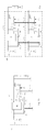
Typically, there are several kinds of power systems using the converters, such as a central power system (CPS) or a distributed power system (DPS). Referring to FIG. 1, FIG. 1 is a system block diagram showing a conventional central power system. In a central power system 10, a single input power source 11 is electrically connected to a power converter 12 and then to a plurality of loadings (RL) 13 (such as electronic devices). For example, the input power source 11 may be a DC power source, and the power converter 12 is employed to convert one DC voltage level to another DC voltage level. Therefore, the input power source 11 can supply power to the loadings 13. However, there are some disadvantages in the conventional central power system, such as high current stress on devices, poor reliability and difficulty in power maintenance, etc.
Referring to FIG. 2, FIG. 2 is a system block diagram showing a conventional distributed power system. In the distributed power system, a single input power source 21 is electrically connected to a plurality of DC-to-DC converters 22 and to a plurality of loadings (RL1, RL2, RL3) 23 (such as electronic devices), wherein the DC-to-DC converters 22 are electrically connected to the respective loadings 23, thereby supplying power to the loadings 23. Although there are some advantages in the conventional distributed power system, such as lower current stress on devices, supporting of N+1 redundancy, ease maintenance and customization with standardized module etc., yet when the single input power source 21 is broken-down or fails to supply power, the whole distributed power system would be useless.
DISCLOSURE OF INVENTION Disclosure
Therefore, an aspect of the present invention is to provide a power system to feed-forward control the paralleling converters, thereby self-regulating the output status of each of the power sources.
Another aspect of the present invention is to provide a power system with a plurality of power sources and a plurality of converters electrically connected thereto respectively in a one-to-one manner, thereby allowing each of the power sources to be replaceable.
According to an embodiment of the present invention, the power system comprises a voltage sharing bus and a plurality of power supply units. The power supply units are electrically connected in parallel and used to provide power to a loading, wherein each of the power supply units is electrically connected to the voltage sharing bus to receive a sharing voltage transmitted by the voltage sharing bus, and comprises: a power converter, a resistor, a first comparator, a current detector, and a second comparator. The power converter is electrically connected to a power source and the load. The resistor is electrically connected to an input terminal of the power converter. The first comparator is used to generate a current reference value in accordance with the difference between the sharing voltage and an input voltage of the power converter, wherein the first comparator is electrically connected to the resistor and the input terminal, and one end of the voltage sharing bus is electrically connected between the resistor and the first comparator. The current detector is used to detect an output current value of the power converter. The second comparator is used to generate the current compensation value in reference value thus that the power converter adjusts the output current value thereof in accordance with the current compensation value.
According to another embodiment of the present invention, the power system comprises a voltage sharing bus, a current sharing bus, and a plurality of power supply units. The power supply units are electrically connected in parallel and used to provide power to a loading, wherein the power supply units are electrically connected to the voltage sharing bus to receive a sharing voltage transmitted by the voltage sharing bus and electrically connected to the current sharing bus to receive a first current reference value transmitted by the current sharing bus, and each of the power supply units comprises a power converter, a feed-forward control (FFC) circuit, and a feedback control (FBC) circuit. The power converter is electrically connected to a power source and the loading. The feed-forward control circuit is used to generate a second current reference value in accordance with the difference between the sharing voltage and an input voltage of the power converter, wherein one end of the voltage sharing bus is electrically connected to the feed-forward control circuit. The feedback control circuit is used to generate a current compensation value in accordance with the first current reference value and the second current reference value, wherein one end of the current sharing bus is electrically connected to the feedback control circuit. The power converter adjusts an output current value thereof in accordance with the current compensation value.
According to a further embodiment of the present invention, the power system comprises a voltage sharing bus, a current sharing bus, a master power supply unit, and at least a slave power supply unit. The voltage sharing bus is used to transmit a sharing voltage. The current sharing bus is used to transmit a first current reference value. The master power supply unit is used to provide power to a loading and provide the first current reference value. The at least one slave power supply unit are electrically connected in parallel with the master power supply unit and used to provide power to the at least one loading. The master power supply unit comprise a first power converter, a first feed-forward control circuit, and a first feedback control circuit. The first power converter is electrically connected to a first power source and the loading. The first feed-forward control circuit is used to generate a second current reference value in accordance with the difference between the sharing voltage and a first input voltage of the power converter. The first feedback control circuit is used to generate the first current reference value, and generate a first current compensation value in accordance with a first output voltage of the first converter and the second current reference value. Then the first power converter adjusts a first output current value thereof in accordance with the first current compensation value. Each of the slave power supply units comprises a second power converter, a second feed-forward control circuit, and a second feedback control circuit. The second power converter is electrically connected to a second power source and the loading. The second feed-forward control circuit is used to generate a third current reference value in accordance with the difference between the sharing voltage and a second input voltage of the second power converter. The second feedback control circuit is used to generate a second current compensation value in accordance with the first current reference value and the third current reference value. The second power converter adjusts a second output current value thereof in accordance with the second current compensation value.
According to a further embodiment of the present invention, the power system comprises a voltage sharing bus, a first power supply unit, and a second power supply. The voltage sharing bus is used to transmit a sharing voltage. The first power supply unit is used to provide power to a loading. The second power supply unit is used to provide power to the loading and electrically connected in parallel with the first power supply. The first power supply comprises a first power converter, a first resistor, and a first comparator. The first power converter is electrically connected to a first power source and the loading, wherein the first power converter comprises a first current output terminal and a first voltage reverence terminal, and the first current output terminal is electrically connected to the loading. The first resistor is electrically connected to a first input terminal of the first power converter. The first comparator is used to generate a first voltage compensation value in accordance with the difference between the sharing voltage and a first input voltage of the first power converter, wherein the first comparator is electrically connected to the second resistor and the input terminal, and one end of the voltage sharing bus is electrically connected between the first resistor and the first comparator. The first power converter adjusts a first output voltage thereof in accordance with the first voltage compensation value. The second power supply unit comprises a second power converter, a second resistor, and a second comparator. The second power converter is electrically connected to a first power source and the loading, wherein the second power converter comprises a second current output terminal and a second voltage reverence terminal, the second current output terminal is electrically connected to the first voltage reference terminal. The second resistor is electrically connected to a second input terminal of the second power converter. The second comparator is used to generate a second voltage compensation value in accordance with the difference between the sharing voltage and a second input voltage of the second power converter, wherein the second comparator is electrically connected to the second resistor and the second input terminal, and another end of the voltage sharing bus is electrically connected between the second resistor and the second comparator. The second power converter adjusts a second output voltage thereof in accordance with the second voltage compensation value.
Therefore, with the application of the power system disclosed in the embodiments of the present invention, the converters are adapted to self-regulate the output current (or output voltage) supplied to the loading respectively according to the input status of each the power sources, thereby enhancing the power efficiency and life time of the power system.
DESCRIPTION OF DRAWINGS
The foregoing aspects and many of the attendant advantages of this invention will become more readily appreciated as the same becomes better understood by reference to the following detailed description, when taken in conjunction with the accompanying drawings, wherein:
FIG. 1 is a system block diagram showing a conventional central power system;
FIG. 2 is a system block diagram showing a conventional distributed power system; and
FIG. 3 is a system block diagram showing a power system according to a first embodiment of the present invention;
FIG. 4 is a circuit diagram power supply unitaccording to a first embodiment of the present invention;
FIG. 5 is a circuit diagram showing one power system according to the first embodiment of the present invention;
FIG. 6 is a circuit diagram showing one power supply unit of a power system according to the first embodiment of the present invention;
FIG. 7 is a system block diagram showing a power system according to a second embodiment through a fifth embodiment of the present invention;
FIG. 8 shows several methods of using current sharing buses according to a second embodiment through a fifth embodiment of the present invention;
FIG. 9 is a circuit diagram showing one power supply unit of a power system according to the second embodiment of the present invention;
FIG. 10 is a circuit diagram showing a power system according to the second embodiment of the present invention;
FIG. 11 is a circuit diagram showing the power system according to the second embodiment of the present invention;
FIG. 12 is a circuit diagram showing a power system according to the second embodiment of the present invention;
FIG. 13 is a circuit diagram showing one power supply unit of a power system according to a third embodiment of the present invention;
FIG. 14 is a circuit diagram showing a power system according to a third embodiment of the present invention;
FIG. 15 is a circuit diagram showing the power system according to the third embodiment of the present invention;
FIG. 16 is a circuit diagram showing a power system according to the third embodiment of the present invention;
FIG. 17 is a circuit diagram showing one power supply unit of a power system 1300 according to a fourth embodiment of the present invention;
FIG. 18 is a circuit diagram showing a power system according to the fourth embodiment of the present invention;
FIG. 19 is a circuit diagram showing the power system according to the fourth embodiment of the present invention;
FIG. 20 is a circuit diagram showing a power system according to the fourth embodiment of the present invention;
FIG. 21 is a circuit diagram showing one power supply unit of a power system according to a fifth embodiment of the present invention;
FIG. 22 is a circuit diagram showing a power system according to the fifth embodiment of the present invention;
FIG. 23 is a circuit diagram showing a power system according to the fifth embodiment of the present invention;
FIG. 24 is a circuit diagram showing the power system according to the fifth embodiment of the present invention;
FIG. 25 is a circuit diagram showing a power system according to a sixth embodiment of the present invention; and
FIG. 26 is a circuit diagram showing a power system according to the sixth embodiment of the present invention.
BEST MODE
In order to make the illustration of the present invention more explicit and complete, the following description is stated with reference to FIG. 3 through FIG. 26.
Referring to FIG. 3. FIG. 3 is a system block diagram showing a power system according to a first embodiment of the present invention. A power system 100 comprises a plurality of power supply units 110, a sharing bus 120 and at least one loading 130. Each of the power supply units 110 comprises a power source 140, a power converter 150, and a converter control circuit 160. The sharing bus 120 is electrically connected to the converter control circuit 160 of each of the power supply units 110 for sharing voltage signal, wherein the sharing bus 120 is a voltage sharing bus. The power source 140 of the power system 100may be DC or AC power sources, such as manpower generators, solar cells, fuel cells, wind-power generators, thermal-power generators, water-power generators, conventional electric power generators or electric cell, to input a source voltage to the power converter 150, thereby supplying power to the loading 130 via the power converter 150.Thepower converter 150 may be DC-to-DC, DC-to-AC, AC-to-DC or AC-to-AC converter for converting the input voltage (DC or AC) to the output voltage (DC or AC). The loading 130 may be any device or apparatus actuated by electric power, such as a motor. Furthermore, a single loading 130 or more than two loadings 130 may be used in the power system 100.
Referring to FIG. 4. FIG. 4 is a circuit diagram showing one power supply unit 110 according to the first embodiment of the present invention. The converter control circuit 160comprises a resistor 160 a, and a first comparator 160 b.The resistor 160 a is electrically connected to the input terminal P, of the power converter 150 thus that the input voltage of the power converter 150 is inputted into the sharing bus 120 via the resistor 160 a. One end of the sharing bus 120 is electrically connected between the resistor 160 a and the first comparator 160 b. The first comparator 160 b is used to generate a current reference value in accordance with the difference between the input voltage of the power converter 150 and a sharing voltage. The sharing voltage is the average of the input voltages inputted into the sharing bus 120 multiplied by weighted values. The power converter 150 comprise a an another converter control circuit 152, wherein the converter control circuit 152 can adjust the output thereof in accordance with the current reference value. In addition, in this embodiment the first comparator 160 b and the second comparator 160 d are more prefer op amplifiers. The power converter of this invention may comprise electrical isolation elements (such as a transformer) or electrical non-isolation elements, thus that the ground voltage GND1 is not necessarily equal to the ground voltage GND2.
In view of the above description, the output current of the converter150 can follow the difference between the voltage provided by the power source 140 and the sharing voltage transmitted by the sharing bus 120.
Referring to FIG. 5. FIG. 5 is a circuit diagram showing a power system 200 according to the first embodiment of the present invention. The power system 200 is a specific example of the power system 100. The power system 200 comprises a power supply unit 110 a, a power supply unit 110 b, the sharing bus 120, and the loading 130, wherein the power supply unit 110 a and power supply unit 110 b is similar to the power supply unit 110. One end of the sharing bus 120 is electrically connected between the resistor 160 a and the first comparator 160 b of the power supply unit 110 a, and another end of the sharing bus 120 is electrically connected between the resistor 160 a and the first comparator 160 b of the power supply unit 110 b. In the power system 200, the power source 140 a provides a first voltage, and the power source 140 b provides a second voltage, wherein the first voltage is higher than the second voltage. When the first voltage (such as 48V) is higher than the second voltage (such as 38V), the power supply unit 110 a can output more current than that outputted by the power supply unit 110 b and keep the power supply unit 110 b do not output the current value exceeding the limitation thereof so that the power supply unit 110 b is protected thereby.
Referring to FIG. 6. FIG. 6 is a circuit diagram showing one power supply unit 310of a power system 300 according to the first embodiment of the present invention. The power system 300 comprises a plurality of power supply units 310. One power supply unit 310 is similar to the power supply unit 110, but the difference is in that the power supply unit 310 further comprises a current detector 160 c, a second comparator 160 d, and an adder 160 e. The current detector 160 c is electrically connected to the output terminal Po of the power converter 150 to detect an output current value of the power converter 150. The adder 160 e is used to calculate the sum of the voltage compensation value and a predetermined voltage Vref, wherein the predetermined voltage Vref is a comparing level. The second comparator 160 d is used to generate a current compensation value in accordance with the difference between the sum and the output current value detected by the current detector 160 c, and then the power converter 150 adjusts the output current thereof in accordance with the current compensation value.
Referring to FIG. 7 and FIG. 8, FIG. 7 is a system block diagram showing a power system 400 according to a second embodiment through a fifth embodiment of the present invention; and FIG. 8 shows several methods of using current sharing buses according to a second embodiment through a fifth embodiment of the present invention. The power system 400 comprises a plurality of power supply units 410, a voltage sharing bus 420 a, a current sharing bus 420 b, and at least one loading 430. Each of the power supply units 410 comprises a power source 440, a power converter 450, a feed-forward control (FFC) circuit 460, and a feedback control (FBC) circuit 470. The voltage sharing bus 420 a is electrically connected to the FFC circuit 460 of each of the power supply units 410, and the current sharing bus 420 b is electrically connected to the FBC circuit 470 of each of the power supply units 410.
The power source 440 may be DC or AC power sources, such as manpower generators, solar cells, fuel cells, wind-power generators, thermal-power generators, water-power generators, conventional electric power generators or electric cell, to input the input voltage to the power converter 450, thereby supplying power to the loading 430 via the power converter 450. The converters 450 may be DC-to-DC, DC-to-AC, AC-to-DC or AC-to-AC converter for converting the input voltage (DC or AC) to the output voltage (DC or AC). The loading 430 may be any device or apparatus actuated by electric power, such as a motor. Furthermore, a single loading or more than two loadings may be used in the power system 400.
In accordance with the second embodiment, the current sharing bus 420 b may be connected by using the method such as dedicated master (DM) method, average current (AC) method, automatic master (AM) method or other suitable method, and the sharing control method may be an inner loop regulation (ILR), an outer loop regulation (OLR), a dual loop regulation (DLR), a single loop regulation (SLR) or other suitable method.
Referring to FIG. 9. FIG. 9 is a circuit diagram showing one power supply unit 510 of a power system 500 according to the second embodiment of the present invention. Power system 500 comprises a plurality of power supply units 510, a voltage sharing bus 520 a, a current sharing bus 520 b, and at least one loading 530. Each of the power supply units 510 comprises a power source 540, a power converter 550, a FFC circuit 560, and a FBC circuit 570. The FFC circuit 560 comprises a resistor 560 a and a first comparator 560 b, and the FBC circuit 570 comprises a second comparator 570 a, a diode 570 b, an adder 570 c, a current detector 570 d, and a third comparator 570 e.In the power system 500, the current sharing bus 520 b is connected in theDM method and the inner loop regulation (ILR) is employed in the power system 500.
In the FFC circuit 560, the resistor 560 a is connected to the input terminal P, of the power converter 550 thus that the input voltage of the power converter 550 is inputted into the voltage sharing bus 520 a via the resistor 560 a. One end of the voltage sharing bus 520 a is electrically connected between the resistor 560 a and the first comparator 560 b. The first comparator 560 b generates a first current reference value in accordance with the difference between the input voltage of the power converter 550 and a sharing voltage. The sharing voltage is the average of the input voltages inputted into the sharing bus 520 a multiplied by weighted values.
In the FBC circuit 570, the second comparator 570 a generates a second current reference value in accordance with the difference between a predetermined voltage Vref and the output voltage of the power converter 550, and forms a regulation loop RL. The positive terminal of the diode 570 b is electrically connected to the second comparator 570 a, and the negative terminal of that is electrically connected to the current sharing bus 520 b, wherein the diode 570 b is used for automatic master method (AM). In each of the power supply units 510, the second current reference value may be inputted into the current sharing bus 520 b via the diode 570 b so that the current sharing bus 520 b can transmitted a third current reference value automatically selected from all the second current reference value. The adder 570 c is used to add the first current reference value and the third current reference value together to generate a total current reference value, and the current detector 570 d is electrically connected to the output terminal Po of the power converter 550 to detect the output current value of the power converter 550. The third comparator 570 e is used to generate a current compensation value in accordance with the difference between the output current value of the power converter 550 and the total current reference value, wherein the third comparator 570 e and the current detector 570 d form a current sharing loop CSL. Then the power converter 550 adjusts the output current thereof in accordance with the current compensation value. The current sharing loop CSL is formed prior to the regulation loop RL, thereby forming the inner loop regulation (ILR). In addition, in the power system 500, the first comparator 560 b, thesecondcomparator 570 a, and the third comparator 570 e are more prefer op amplifiers.
In view of the above description, the output current of the converter 550 can follow the voltage provide by the current sharing bus 520 b and the difference between the voltage provided by the power source 540 and the sharing voltage transmitted by the voltage sharing bus 520 a.
Referring to FIG. 10. FIG. 10 is a circuit diagram showing a power system 600according to the second embodiment of the present invention. The power system 600 is a specific example of the power system 500. The power system 600 comprises a power supply unit 510 a, a power supply unit 510 b, a voltage sharing bus 520 a, a current sharing bus 520 b, and a loading 530, wherein the power supply unit 510 a and the power supply unit 510 b are similar to the power supply unit 510. One end of the voltage sharing bus 520 a is electrically connected between the resistor 560 a and the first comparator 560 b of the power supply unit 510 a, and another end of the voltage sharing bus 520 a is electrically connected between the resistor 560 a and the first comparator 560 b of the power supply unit 510 b.One end of the current sharing bus 520 b is electrically connected between the diode 570 b and the adder 570 c of the power supply unit 510 a, and another end of the current sharing bus 520 b is electrically connected between the diode 570 b and the adder 570 c of the power supply unit 510 b. In the power system 600, the power source 540 a is used to provide a first voltage and the power source 540 b is used to provide a second voltage, and the first voltage is higher than the second voltage. For example, when the first voltage (such as 48V) provided is higher than the second voltage (such as 38V), the FFC circuit 560 of the power supply unit 510 a and that of the power supply unit 510 b enable the output current value of the power supply unit 510 a to be always higher than that of the power supply unit 510 b, and keep the output current of the power supply unit 510 b lower than the limitation thereof, thus that the power supply unit 510 b is protected, and a output current difference between the power supply unit 510 a and the power supply unit 510 b in the power system 600 is smaller than that between the power supply unit 110 a and the power supply unit 110 b in the power system 200.
Referring to FIG. 11. FIG. 11 is a circuit diagram showing a power system 700 according to the second embodiment of the present invention. The power system 700 is similar to the power system 500, but the difference is in that each of the power supply units 710 of the power system 700 comprises a resistor 570 g instead of the diode 570 b.In the power system 700, the average current (AC) method and the inner loop regulation (ILR) are employed, thus that the third current reference value is the average of the second current reference values inputted into the current sharing bus 520 b multiplied by weighted values.
Referring to FIG. 12. FIG. 12 is a circuit diagram showing a power system 800 according to the second embodiment of the present invention. The power system 800 comprises a master power supply unit 810 a, at least one slave power supply unit 810 b, the voltage sharing bus 520 a, the current sharing bus 520 b, and the loading 530. The master power supply unit 810 a is similar to the power supply unit 510, but the difference is in that the master power supply unit 810 a do not have the diode 570 b, and one end of the current sharing bus 520 b is connected between the first comparator 570 a and the adder 570 c of the master power supply unit 810 a. In addition, the slave power supply unit 810 b is similar to the master power supply unit 810 a, but the difference is in that the slave power supply unit 810 b do not have the first comparator 570 a, and one end of the current sharing bus 520 b is connected to the adder 570 c of the slave power supply unit 810 b.In the power system 800, the dedicated master (DM) method and the inner loop regulation (ILR) is employed, thus that the third current reference value is the second current reference value provided by the first comparator 570 a of the master power supply unit 810 a.
Referring to FIG. 13. FIG. 13 is a circuit diagram showing one power supply unit 910 of a power system 900 according to a third embodiment of the present invention. Power system 900 comprises a plurality of power supply units 910, a voltage sharing bus 920 a, a current sharing bus 920 b, and at least one loading 930. Each of the power supply units 910 comprises a power source 940, a converter 950, a FFC circuit 960, and a FBC circuit 970. The FFC circuit 960 comprises a resistor 960 a and a first comparator 960 b, and the FBC circuit 970 comprises a second comparator 970 a, a diode 970 b, an adder 970 c, a current detector 970 d, and a third comparator 970 e. In the power system 900, the current sharing bus 920 b is connected in the AM method and the outer loop regulation (OLR) is employed.
In the FFC circuit 960, the resistor 960 a is connected to the input terminal P, of the power converter 950 thus that an input voltage of the power converter 950 is inputted into the voltage sharing bus 920 a via the resistor 960 a. One end of the voltage sharing bus 920 a is electrically connected between the resistor 960 a and the first comparator 960 b. Thefirst comparator 960 b generates a first current reference value in accordance with the difference between the input voltage of the power converter 950 and a sharing voltage. The sharing voltage is the average of the input voltages inputted into the sharing bus 920 a multiplied by weighted values.
In the FBC circuit 970,the current detector 970 d is electrically connected to the output terminal Po of the power converter 950 to detect the output current value of the power converter 950.The positive terminal of the diode 970 b is electrically connected to the current detector 970 d, and the negative terminal of that is electrically connected to the current sharing bus 920 b, wherein the diode 970 b is used for automatic master method. In each of the power supply units 910, the output current value of the power converter 950 may be inputted into the current sharing bus 920 b via the diode 970 b so that the current sharing bus 920 b can transmit a second current reference value automatically selected from all the output current values inputted into the current sharing bus 920 b.The second comparator 970 a generates a third current reference value in accordance with the difference between the second current reference value and the output current of the power converter 950, and forms a current sharing loop CSL. The adder 970 c is used to add the first current reference value, the third current reference value, and a predetermined voltage Vref to generate a total current reference value. The third comparator 970 e is used to generate a current compensation value in accordance with the difference between the output voltage value of the power converter 950 and the total current reference value, forms a regulation loop RL. Then the power converter 950 adjusts the output current thereof in accordance with the current compensation value. The regulation loop RL is formed prior to the current sharing loop CSL, thereby forming the outer loop regulation (OLR). In addition, in the power system 900, the first comparator 960 b, the second comparator 970 a, and the third comparator 970 e are more prefer op amplifiers.
In view of the above description, the output current of the converter 950 can follow the voltage transmitted by the current sharing bus 920 b and the difference between the voltage provided by the power source 940 and the sharing voltage transmitted by the voltage sharing bus 920 a. It is noted that the predetermined voltage is not necessary in the third embodiment.
Referring to FIG. 14. FIG. 14 is a circuit diagram showing a power system 1000 according to the third embodiment of the present invention. The power system 1000 is a specific example of the power system 900. The power system 1000 comprises a power supply unit 910 a, a power supply unit 910 b, a voltage sharing bus 920 a, a current sharing bus 920 b, and a loading 930, wherein the power supply unit 910 a and the power supply unit 910 b is similar to the power supply unit 910. One end of the voltage sharing bus 920 a is electrically connected between the resistor 960 a and the first comparator 960 b of the power supply unit 910 a, and another end of the voltage sharing bus 920 a is electrically connected between the resistor 960 a and the first comparator 960 b of the power supply unit 910 b. One end of the current sharing bus 920 b is electrically connected between the diode 970 b and the comparator 970 a of the power supply unit 910 a, and another end of the current sharing bus 920 b is electrically connected between the diode 970 b and the comparator 970 a of the power supply unit 910 b. The function of the power system 1000 is similar to that of the power system 600. For example, when a first voltage (such as 48V) provided by a power source 940 a is higher than a second voltage (such as 38V) provided by a power source 940 b, the FFC circuit 960 of the power supply unit 910 a and that of the power supply unit 910 b enable the output current value of the power supply unit 910 a to be always higher than that of the power supply unit 910 b and keep the output current of the power supply unit 910 b lower than the limitation thereof, thus that the power supply unit 910 b is protected, and a output current difference between the power supply unit 910 a and the power supply unit 910 b in the power system 900 is smaller than that between the power supply unit 910 a and the power supply unit 910 b in the power system 200.
Referring to FIG. 15. FIG. 15 is a circuit diagram showing a power system 1100 according to the third embodiment of the present invention. The power system 1100 is similar to the power system 900, but the difference is in that each of the power supply units 1010 of the power system 1000 comprises a resistor 970 g instead of the diode 970 b.In the power system 1100, the average current method and the outer loop regulation are employed, thus that the second current reference value is the average of the second current reference values inputted into the current sharing bus 920 b multiplied by weighted values.
Referring to FIG. 16. FIG. 16 is a circuit diagram showing a power system 1200 according to the third embodiment of the present invention. The power system 1200 comprises a master power supply unit 1210 a, at least one slave power supply unit 1210 b, the voltage sharing bus 920 a, the current sharing bus 920 b, and the loading 930. The master power supply unit 1210 a is similar to the power supply unit 910, but the difference is in that the master power supply unit 1210 a do not have the first comparator 970 a and the diode 970 b, and one end of the current sharing bus 920 b is connected to the current detector 970 d of the master power supply unit 1210 a. In addition, the slave power supply unit 1210 b is similar to the power supply unit 910, but the difference is in that the slave power supply unit 1210 b do not have the diode 970 b, and one end of the current sharing bus 920 b is connected to the first comparator 970 a. In the power system 1200, the dedicated master (DM) method and the outer loop regulation (OLR) is employed, thus that the second current reference value is the output current value detected by the current detector 970 d of the master power supply unit 1210 a.
Referring to FIG. 17. FIG. 17 is a circuit diagram showing one power supply unit1310 of a power system 1300 according to a fourth embodiment of the present invention. Power system 1300 comprises a plurality of power supply units 1310, a voltage sharing bus 1320 a, a current sharing bus 1320 b, and at least one loading 1330. Each of the power supply units 1310 comprises a power source 1340, a converter 1350, a FFC circuit 1360, and a FBC circuit 1370. The FFC circuit 1360 comprises a resistor 1360 a and a first comparator 1360 b, and the FBC circuit 1370 comprises a second comparator 1370 a, a diode 1370 b, an adder 1370 c, a current detector 1370 d, and a third comparator 1370 e.In the power system 1300, the current sharing bus 1320 b is connected in the AM method method and the dual loop regulation (DLR) is employed in the power system 1300.
In the FFC circuit 1360, the resistor 1360 a is connected to the input terminal P, of the power converter 1350 thus that the input voltage of the power converter 1350 is inputted into the voltage sharing bus 1320 a via the resistor 1360 a. One end of the voltage sharing bus 1320 a is electrically connected between the resistor 1360 a and the first comparator 1360 b. The first comparator 1360 b generates a first current reference value in accordance with the difference between the input voltage of the power converter 1350 and a sharing voltage. The sharing voltage is the average of the input voltages inputted into the sharing bus 1320 a multiplied by weighted values.
In the FBC circuit 1370, the second comparator 1370 a generates a second current reference value in accordance with the difference between a predetermined voltage Vref and the output voltage of the power converter 1350, and forms a regulation loop RL. The current detector 1370 d is electrically connected to the output terminal Po of the power converter 1350 to detect an output current value of the power converter 1350. The positive terminal of the diode 1370 b is electrically connected to the current detector 1370 d and the negative terminal of that is electrically connected to the current sharing bus 1320 b, wherein the diode 1370 b is used for automatic master method. In each of the power supply units 1310, a output current value of the converter 1350 may be inputted into the current sharing bus 1320 b via the diode 1370 b so that the current sharing bus 1320 b can transmitted a third current reference value automatically selected from all the output current values of the power supply units 1310. The third comparator 1370 e is used to generate a fourth current reference value in accordance with the difference between the third current reference value and the output current value of the power converter 1350. The adder 1370 c is used to add the first current reference, the second current reference, and the fourth current reference value together to generate a current compensation reference value. Then the power converter 1350 adjusts the output current thereof in accordance with the current compensation value. The current sharing loop CSL and the regulation loop RL are connected in parallel, thereby forming the dual loop regulation (DLR). In addition, in the power system 1300, the first comparator 1360 b, the second comparator1370 a, and the third comparator 1370 e are more prefer op amplifiers.
In view of the above description, the output current of the converter 1350 can follow the voltage transmitted by the current sharing bus 1320 b, and the difference between the voltage provided by the power source 1340 and the sharing voltage transmitted by the voltage sharing bus 1320 a.
Referring to FIG. 18. FIG. 18 is a circuit diagram showing a power system 1400 according to the fourth embodiment of the present invention. The power system 1400 is a specific example of the power system 1300. The power system 1400 comprises a power supply unit 1410 a, a power supply unit 1410 b, the voltage sharing bus 1320 a, a current sharing bus 1320 b, and the loading 1330, wherein the power supply unit 1410 a and the power supply unit 1410 b is similar to the power supply unit 1310. The power source 1340 a is used to provide a first voltage, and the power source 1340 b is used to provide a second voltage. One end of the voltage sharing bus 1320 a is electrically connected between the resistor 1360 a and the first comparator 1360 b of the power supply unit 1410 a, and another end of the voltage sharing bus 1320 a is electrically connected between the resistor 1360 a and the first comparator 1360 b of thepower supply unit 1410 b. One end of the current sharing bus 1320 b is electrically connected between the diode 1370 b and and the third comparator 1370 e of the power supply unit 1410 a, and another end of the current sharing bus 1320 b is electrically connected between the diode 1370 b and the third comparator 1370 e of the power supply unit 1410 b. The function of the power system 1400 is similar to that of the power system 1000. For example, when a first voltage (such as 48V) provided by a power source 1340 a is higher than a second voltage (such as 38V) provided by a power source 1340 b, the FFC circuit 1360 of the power supply unit 1410 a and that of the power supply unit 1410 b enable the output current value of the power supply unit 1410 a to be always higher than that of the power supply unit 1410 b and keep the output current of the power supply unit 1410 b lower than the limitation thereof, thus that the power supply unit 1410 b is protected, and a output current difference between the power supply unit 1410 a and the power supply unit 1410 b in the power system 1400 is smaller than that between the power supply unit 1410 a and the power supply unit 1410 b in the power system 200.
Referring to FIG. 19. FIG. 19 is a circuit diagram showing a power system 1500 according to the fourth embodiment of the present invention. The power system 1500 is similar to the power system 1300, but the difference is in that each of the power supply units 1510 of the power system 1500 comprises a resistor 1370 g instead of the diode 1370 b. In the power system 1500, the average current (AC) method and the dual loop regulation (DLR) are employed, thus that the third current reference value is the average of all the output current values detected by the current detectors 1370 d multiplied by weighted values.
Referring to FIG. 20. FIG. 20 is a circuit diagram showing a power system 1600 according to the fourth embodiment of the present invention. The power system 1600 comprises a master power supply unit 1610 a, at least one slave power supply unit 1610 b, the voltage sharing bus 1320 a, the current sharing bus 1320 b, and the loading 1330. The master power supply unit 1610 a is similar to the power supply unit 1310, but the difference is in that the master power supply unit 1610 a does not have the third comparator 1370 e and the diode 1370 b, and one end of the current sharing bus 1320 b is connected to the current detector 1370 d of the master power supply unit 1610 a. In addition, the slave power supply unit 1610 b is similar to the power supply unit 1310, but the difference is in that the slave power supply unit 1610 b do not have the diode 1370 b, and one end of the current sharing bus 1320 b is connected to the third comparator 1370 e of the slave power supply unit 1610 b. In the power system 1600, the dedicated master (DM) method and the dual loop regulation (DLR) is employed, thus that the third current reference value is the output current value detected by the current detector 1370 d of the master power supply unit 1610 a.
Referring to FIG. 21. FIG. 21 is a circuit diagram showing one power supply unit 1710 of the power system 1700 according to a fifth embodiment of the present invention. Power system 1700 comprises a plurality of power supply units 1710, a voltage sharing bus 1720 a, a current sharing bus 1720 b, and at least one loading 1730. Each of the power supply units 1710 comprises a power source 1740, a converter 1750, a FFC circuit 1760, and a FBC circuit 1770. The FFC circuit 1760 comprises a resistor 1760 a and a first comparator 1760 b, and the FBC circuit 1770 comprises a second comparator 1770 a, a diode 1770 b, an adder 1770 c, and a current detector 1770 d. In the power system 1700, the current sharing bus 1720 b is connected in the AM method and the single loop regulation (SLR) is employed in the power system 1700.
In the FFC circuit 1760, the resistor 1760 a is connected to the input terminal P, of the power converter 1750 thus that the input voltage of the power converter 1750 is inputted into the voltage sharing bus 1720 a via the resistor 1760 a. One end of the voltage sharing bus 1720 a is electrically connected between the resistor 1760 a and the first comparator 1760 b. The first comparator 1760 b generates a first current reference value in accordance with the difference between the input voltage of the power converter 1750 and a sharing voltage. The sharing voltage is the average of the input voltages inputted into the sharing bus 1720 a or the average of the input voltages inputted into the sharing bus 1720 a multiplied by weighted values.
In the FBC circuit 1770, the current detector 1770 d is electrically connected to the output terminal Po of the power converter 1370 to detect the output current value of the power converter 1350.The positive terminal of the diode 1770 b is electrically connected to the current detector 1770 d and the negative terminal of that is electrically connected to the current sharing bus 1720 b, wherein the diode 1770 b is used for automatic master method. In each of the power supply units 1710, the output current value of the power converter 1750 may be inputted into the current sharing bus 1720 b via the diode 1770 b so that the current sharing bus 1720 b can transmitted a second current reference value selected automatically from all the output current values inputted into the current sharing bus 1720 b. The second comparator 1770 a generates a third current reference value in accordance with the difference between the second current reference value and the output current value of the power converter 1750. The adder 1770 c is used to add the first current reference and the third current reference value together to generate a current compensation value. Then the power converter 1750 adjusts the output current thereof in accordance with the current compensation value. Because the power system does not comprise regulation loop RL, the single loop regulation is formed. In addition, in the power system 1700, the first comparator 1760 b, the second comparator 1770 a, and the third comparator 1770 e are more prefer op amplifiers.
In view of the above description, the output current of the converter 1750 can follow the voltage transmitted by the current sharing bus 1720 b, and the difference between the voltage provided by the power source 1740 and the sharing voltage transmitted by the voltage sharing bus 1720 a.
Referring to FIG. 22. FIG. 22 is a circuit diagram showing a power system 1800 according to the fifth embodiment of the present invention. The power system 1800 is a specific example of the power system 1700. The power system 1800 comprises a power supply unit 1810 a, a power supply unit 1810 b, the voltage sharing bus 1720 a, a current sharing bus 1720 b, and the loading 1730, wherein the power supply unit 1810 a and power supply unit 1810 b are similar to the power supply unit 1710. The power source 1740 a is used to provide a first voltage, and the power source 1740 b is used to provide a second voltage. One end of the voltage sharing bus 1720 a is electrically connected between the resistor 1760 a and the first comparator 1760 b of the power supply unit 1810 a, and another end of the voltage sharing bus 1720 a is electrically connected between the resistor 1760 a and the first comparator 1760 b of the power supply unit 1810 b.One end of the current sharing bus 1720 b is electrically connected between the diode 1770 b and the second comparator 1770 a of the power supply unit 1810 a, and another end of the current sharing bus 1720 b is electrically connected between the diode 1770 b and the second comparator 1770 a of the power supply unit 1810 b.The function of the power system 1800 is similar to that of the power system 1000. For example, when a first voltage (such as 48V) provided by a power source 1740 a is higher than a second voltage (such as 38V) provided by a power source 1370 b, the FFC circuit 1760 of the power supply unit 1810 a and that of the power supply unit 1810 b enable the output current value of the power supply unit 1710 a to be always higher than that of the power supply unit 1810 b and keep the output current of the power supply unit1810 b lower than the limitation thereof, thus that the power supply unit 1810 b is protected, and a output current difference between the power supply unit 1810 a and the power supply unit 1810 b in the power system 1800 is smaller than that between the power supply unit 1810 a and the power supply unit 1810 b in the power system 200.
Referring to FIG. 23. FIG. 23 is a circuit diagram showing a power system 1900 according to the fifth embodiment of the present invention. The power system 1900 is similar to the power system 1700, but the difference is in that each of the power supply units 1910 of the power system 1900 comprises a resistor 1770 g instead of the diode 1770 b. In the power system 1900, the average current method and the single loop regulation (SLR) are employed, thus that the second current reference value is the average of all the output current values detected by the current detectors 1770 d.
Referring to FIG. 24. FIG. 24 is a circuit diagram showing a power system 2000 according to the fifth embodiment of the present invention. The power system 2000 comprises a master power supply unit 2010 a, at least one slave power supply unit 2010 b, the voltage sharing bus 1720 a, the current sharing bus 1720 b, and the loading 1730. The master power supply unit 2010 a is similar to the power supply unit 910 a, but the difference is in that the FBC circuit 970 of the master power supply unit 2010 a does not comprises the second comparator 970 a and the diode 970 b, wherein the current detector is used to detect the output current of the power converter 950; the adder 970 c is used to add the first current reference value and a predetermined voltage Vref together to generate a fifth current reference value; and third comparator 970 e is used to generate a current compensation value in accordance with the difference between the fifth current reference value and the output voltage value of the power converter 950 of the master power supply unit 2010 a. Then the power converter 950 of the master power supply unit 2010 a adjusts the output current thereof in accordance with the current compensation value. In addition, one end of the current sharing bus 1720 b is electrically connected to the current detector 970 d to transmit the output current value of the power converter 950 of the master power supply unit 2010 a. The slave power supply unit 2010 b is similar to the power supply unit 1710, but the difference is in that the slave power supply unit 2010 b do not have the diode 1770 b, and one end of the current sharing bus 1720 b is connected to the second comparator 1770 a. In the power system 2000, the dedicated master method and single loop regulation is employed, thus that the second current reference value is the output current value detected by the current detector 970 d of the master power supply unit 2010 a.
Referring to FIG. 25. FIG. 25 is a circuit diagram showing a power system 2100 according to a sixth embodiment of the present invention. The power system 2100 comprises a power supply unit 2110 a, a power supply unit 2110 b, a voltage sharing bus 2120, and at least a loading 2130. The power supply unit 2110 a comprises a power source 2140, a power converter 2150 a, and a FFC circuit 2160, wherein the power converter 2150 a comprises a current output terminal and a voltage reference terminal, and the current output terminal is connected to the loading 2130 to provide power. The power supply unit 2110 b comprises the power source 2140, a power converter 2150 b, and the FFC circuit 2160, wherein the power converter 2150 b comprises a current output terminal and a voltage reference terminal. The current output terminal of the converter 2150 b is electrically connected to the voltage reference terminal of the converter 2150 a, and the voltage reference terminal of the converter 2150 b is electrically connected to ground voltage.
The FFC circuit 2160 comprises a resistor 2160 a, and a first comparator 2160 b. Because the function of the FFC circuit 2160 of the power supply unit 2110 a and that of the power supply unit 2110 b are the same, the following description takes the FFC circuit 2160 of the power supply unit 2110 a as an example for explanation. In the FFC circuit 2160 of the power supply unit 2110 a, the resistor 2160 a is connected to the input terminal P, of the power converter 2150 a thus that the input voltage of the power converter 2150 a is inputted into the voltage sharing bus 2120 via the resistor 2160 a. One end of the voltage sharing bus 2120 is electrically connected between the resistor 2160 a and the first comparator 2160 b. The first comparator 2160 b generates a voltage compensation value in accordance with the difference between the input voltage of the power converter 2150 a and a sharing voltage. The sharing voltage is the average of the input voltages inputted into the sharing bus 2120 multiplied by weighted values. Then the power converter 2150 a adjusts the output voltage Vo thereof in accordance with the voltage compensation value.
In the power system 2100, the power source 2140 of the power supply unit 2110 a provides a first voltage, and the power source 2140 of the power supply unit 2110 b provides a second voltage, wherein the first voltage is higher than the second voltage. The function of the power system 2100 is described in the followings. For example, when the first voltage (such as 48V) is higher than the second voltage (such as 38V), the FFC circuit 2160 of the power supply unit 2110 a and that of the power supply unit 2110 b enable the output voltage value of the power supply unit 2110 a to be always higher than that of the power supply unit 2110 b so that the power supply unit 2110 b do not output the voltage exceeding the limitation thereof.
Referring to FIG. 26. FIG. 26 is a circuit diagram showing a power system 2200 according to the third embodiment of the present invention. The power system 2200 is similar to the power system 2100, but the difference is in that the power system 2200 further comprise a third power supply unit 2110. The third power supply unit 2110 c is similar to the first power supply unit 2110 a, but the difference is in that the current output terminal of the power converter 2150 c is electrically connected to the voltage reference terminal of the power converter 2150 a, and the voltage reference terminal of the power converter 2150 c is electrically connected to the current output terminal of the power converter 2150 b. Because the advantages of the power system 2200 are similar to the power system 2100, the advantages of the power system 2200 are not described here. In addition, the amount of the third power supply unit is not limited here, connecting every two adjacent ones of the third power supply units can achieve the same advantages with that of the power system 2200.
In view of the above description, the output current of the converter 2150 can follow the difference between the voltage provided by the power source 2140 and the sharing voltage transmitted by the voltage sharing bus 2120.
Therefore, the power system shown in the respective embodiments of the present invention provide a plurality of power sources connected in parallel or serial, so as to prevent the whole power system from not working when a single power source is poor or fails. Further, the converters are adapted to self-regulate the output current (or output voltage) supplied to the loading respectively according to the input status of each the power sources, i.e. the power source with higher input status can supply more power to the loading, and the power source with lower input status can avoid supplying too much power, thereby enhancing the power efficiency and life time of the power system.
As is understood by a person skilled in the art, the foregoing embodiments of the present invention are strengths of the present invention rather than limiting of the present invention. It is intended to cover various modifications and similar arrangements included within the spirit and scope of the appended claims, the scope of which should be accorded the broadest interpretation so as to encompass all such modifications and similar structure.

Claims (36)

1. A power system, comprising:
a voltage sharing bus used to transmit a sharing voltage; and
a plurality of power supply units electrically connected in parallel and used to provide power to a loading, wherein each of the power supply units is electrically connected to the voltage sharing bus to receive the sharing voltage, and comprises:
a power converter electrically connected to a power source and the loading;
a resistor electrically connected to a input terminal of the power converter;
a first comparator used to generate a current reference value in accordance with the difference between the sharing voltage and an input voltage of the power converter, wherein the first comparator is electrically connected to the resistor and the input terminal, and one end of the voltage sharing bus is electrically connected between the resistor and the first comparator;
a current detector used to detect an output current value of the power converter; and
a second comparator used to generate the current compensation value in accordance with the difference between the output current value and the current reference value thus that the power converter adjusts the output current value thereof in accordance with the current compensation value.
2. The power system as claimed in claim 1, wherein each of the power supply units further comprises an adder electrically connected between the power converter and the second comparator, wherein the adder is used to add the current reference value and a predetermined voltage value together.
3. The power system as claimed in claim 1, wherein the sharing voltage is the average of the input voltages of the power converters multiplied by a plurality of weighted values.
4. The power system as claimed in claim 1, wherein the power source is a manpower generator, a solar cell, a fuel cells, a wind-power generator, a thermal-power generator, a water-power generator, a electric power generator and a electric cell.
5. A power system, comprising:
a voltage sharing bus used to transmit a sharing voltage;
a current sharing bus used to transmit a first current reference; and
a plurality of power supply units electrically connected in parallel and used to provide power to a loading, wherein the power supply units are electrically connected to the voltage sharing bus to receive the sharing voltage and electrically connected to the current sharing bus to receive the first current reference value, and each of the power supply units comprises:
a power converter electrically connected to a power source and the loading;
a feed-forward control (FFC) circuit used to generate a second current reference value in accordance with the difference between the sharing voltage and an input voltage of the power converter, wherein one end of the voltage sharing bus is electrically connected to the feed-forward control circuit; and
a feedback control (FBC) circuit used to generate a current compensation value in accordance with the first current reference value and the second current reference value, wherein one end of the current sharing bus is electrically connected to the feedback control circuit;
wherein the power converter adjusts an output current value thereof in accordance with the current compensation value.
6. The power system as claimed in claim 5, wherein the feed-forward control circuit comprises:
a resistor electrically connected to a input terminal of the power converter; and
a first comparator used to generate the second current reference value in accordance with the difference between the sharing voltage and an input voltage of the power converter, wherein the first comparator is electrically connected to the resistor and the input terminal, and one end of the voltage sharing bus is electrically connected between the resistor and the first comparator.
7. The power system as claimed in claim 5, wherein the feedback control circuit comprises:
a first comparator used to generate a third current reference value in accordance with the difference between a output voltage of the converter and a predetermined voltage;
a diode, wherein a positive terminal of the diode is electrically connected to the first comparator and a negative terminal of the diode is electrically connected to the end of the current sharing bus;
an adder used to add the first current reference value and the second current reference value together to generate a total current reference value; and
a current detector used to detect the output current value of the power converter;
a second comparator used to generate the current compensation value in accordance with the difference between the total current reference value and the output current value of the power converter.
8. The power system as claimed in claim 5, wherein the feedback control circuit comprises:
a first comparator used to generate a third current reference value in accordance with the difference between a output voltage of the converter and a predetermined voltage;
a resistor electrically connected between the first comparator and the end of the current sharing bus;
an adder used to add the first current reference value and the second current reference value together to generate a total current reference value;
a current detector used to detect the output current value of the power converter;
a second comparator used to generate the current compensation value in accordance with the difference between the total current reference value and the output current value of the power converter.
9. The power system as claimed in claim 5, wherein the feedback control circuit comprises:
a current detector used to detect the output current value of the power converter;
a diode, wherein a positive terminal of the diode is electrically connected to the current detector and a negative terminal of the diode is electrically connected to the end of the current sharing bus;
a first comparator electrically connected to the current detector and the end of the current sharing bus, wherein the first comparator is used to generate a third current reference value in accordance with the difference between output current value and the second current reference value;
an adder used to add the third current reference value and the second current reference value together to generate a total current reference value; and
a second comparator used to generates the current compensation value in accordance with the total current reference value and the output current value of the power converter.
10. The power system as claimed in claim 9, wherein the adder further adds a predetermined voltage to the sum of the third current reference value and the second current reference value together.
11. The power system as claimed in claim 5, wherein the feedback control circuit comprises:
a current detector used to detect the output current value of the power converter;
a resistor, electrically connected between the current detector and the end of the current sharing bus;
a first comparator connected to the current detector and the end of the current sharing bus, wherein the first comparator is used to generate a third current reference value in accordance with the difference between output current value and the second current reference value;
an adder used to add the third current reference value and the second current reference value together to generate a total current reference value; and
a second comparator used to generates the current compensation value in accordance with the total current reference value and the output current value of the power converter.
12. The power system as claimed in claim 11, wherein the adder further adds a predetermined voltage on the sum of the third current reference value and the second current reference value together.
13. The power system as claimed in claim 5, wherein the feedback control circuit comprises:
a current detector used to detect the output current value of the power converter;
a diode, wherein a positive terminal of the diode is electrically connected to the current detector and a negative terminal of the diode is electrically connected to the end of the current sharing bus;
a first comparator electrically connected to the current detector and the end of the current sharing bus, wherein the first comparator is used to generate a third current reference value in accordance with the difference between the output current value of the converter and the first current reference value;
a second comparator used to generates a fourth current reference value in accordance with the difference between the a output voltage value of the converter and a predetermined voltage; and
an adder used to add the second current reference value, the third current reference value, and the fourth current reference value together to generate the current compensation value.
14. The power system as claimed in claim 5, wherein the feedback control circuit comprises:
a current detector used to detect the output current value of the power converter;
a diode, wherein a positive terminal of the diode is electrically connected to the current detector and a negative terminal of the diode is electrically connected to the end of the current sharing bus;
a first comparator electrically connected to the current detector and the end of the current sharing bus, wherein the first comparator is used to generate a third current reference value in accordance with the difference between the output current value of the converter and the first current reference value; and
an adder used to add the second current reference value, and the third current reference value together to generate the current compensation value.
15. The power system as claimed in claim 5, wherein the feedback control circuit comprises:
a current detector used to detect the output current value of the power converter;
a resistor electrically connected between the current detector and the end of the current sharing bus;
a first comparator electrically connected to the current detector and the end of the current sharing bus, wherein the first comparator is used to generate a third current reference value in accordance with the difference between the output current value of the converter and the first current reference value; and
an adder used to add the second current reference value, and the third current reference value together to generate the current compensation value.
16. The power system as claimed in claim 5, wherein the sharing voltage is the average of the input voltages of the power converters multiplied by a plurality of weighted values.
17. The power system as claimed in claim 5, wherein the power source is a manpower generator, a solar cell, a fuel cells, a wind-power generator, a thermal-power generator, a water-power generator, a electric power generator and a electric cell.
18. A power system, comprising:
a voltage sharing bus used to transmit a sharing voltage;
a current sharing bus used to transmit a first current reference value;
a master power supply unit used to provide power to at least one loading and provide the first current reference value, wherein the master power supply unit comprises:
a first power converter electrically connected to a first power source and the at least one loading;
a first feed-forward control (FFC) circuit used to generate a second current reference value in accordance with the difference between the sharing voltage and a first input voltage of the power converter; and
a first feedback control (FBC) circuit used to generate the first current reference value, and generate a first current compensation value in accordance with a first output voltage of the first converter and the second current reference value;
wherein the first power converter adjusts a first output current value thereof in accordance with the first current compensation value; and
at least one slave power supply unit electrically connected in parallel with the and used to provide power to the at least one loading, wherein the slave power supply units are electrically connected to the voltage sharing bus to receive the sharing voltage and electrically connected to the current sharing bus to receive the first current reference value, and each of the power supply units comprises:
a second power converter electrically connected to a second power source and the at least one loading;
a second feed-forward control (FFC) circuit used to generate a third current reference value in accordance with the difference between the sharing voltage and a second input voltage of the second power converter; and
a second feedback control (FBC) circuit used to generate a second current compensation value in accordance with the first current reference value and the third current reference value;
wherein the second power converter adjusts a second output current value thereof in accordance with the second current compensation value.
19. The power system as claimed in claim 18, wherein the first feed-forward control circuit comprises:
a resistor electrically connected to a input terminal of the first power converter; and
a first comparator used to generate the second current reference value in accordance with the difference between the sharing voltage and a first input voltage of the first power converter, wherein the first comparator is electrically connected to the resistor and the input terminal, and one end of the voltage sharing bus is electrically connected between the resistor and the first comparator.
20. The power system as claimed in claim 18, wherein the second feed-forward control circuit comprises:
a resistor electrically connected to a input terminal of the second power converter; and
a first comparator used to generate the third current reference value in accordance with the difference between the sharing voltage and a second input voltage of the second power converter, wherein the first comparator is electrically connected to the resistor and the input terminal, and one end of the voltage sharing bus is electrically connected between the resistor and the first comparator.
21. The power system as claimed in claim 18, wherein the first feedback control circuit comprises:
a first comparator used to generate the first current reference value in accordance with the difference between the output voltage of the first converter and a predetermined voltage;
an adder used to add the first current reference value and the second current reference value together to generate a total current reference value; and
a current detector used to detect the output current value of the first power converter;
a second comparator used to generate the first current compensation value in accordance with the difference between the total current reference value and the output current value of the power converter.
22. The power system as claimed in claim 18, wherein the second feedback control circuit comprises:
an adder used to add the first current reference value and the second current reference value together to generate a total current reference value; and
a current detector used to detect the output current value of the second power converter;
a first comparator used to generate the second current compensation value in accordance with the difference between the total current reference value and the output current value of the power converter.
23. The power system as claimed in claim 18, wherein the first feedback control circuit comprises:
a current detector used to detect a output current value of the first power converter to generate the first current reference value;
a first comparator used to generate the first current compensation value in accordance with the difference between the output voltage of the first converter and the second current reference value.
24. The power system as claimed in claim 18, wherein the first feedback control circuit comprises:
a current detector used to detect a output current value of the first power converter to generate the first current reference value;
an adder used to add the first current reference value and the second current reference value together to generate a total current reference value; and
a first comparator used to generate the first current compensation value in accordance with the difference between the output voltage of the first converter and the second current reference value.
25. The power system as claimed in claim 18, wherein the second feedback control circuit comprises:
a first current detector used to detect the second output current value of the second converter;
a first comparator used to generate a fourth current reference value in accordance with the difference between the first current reference value and the second output current value of the second power converter;
an adder used to add the fourth current reference value and the third current reference value together to generate a total current reference value; and
a second comparator used to generate the second current compensation value in accordance with the difference between the total current reference value and a second output voltage of the second power converter.
26. The power system as claimed in claim 18, wherein the first feedback control circuit comprises:
a current detector used to detect a output current value of the first power converter to generate the first current reference value;
a first comparator used to generate a fourth current reference value in accordance with the difference between the output voltage value of the first converter and a predetermined voltage value; and
an adder used to add the fourth current reference value and the second current reference value together to generate the first current compensation value.
27. The power system as claimed in claim 18, wherein the second feedback control circuit comprises:
a first current detector used to detect the second output current value of the second converter;
a first comparator used to generate a fourth current reference value in accordance with the difference between the first current reference value and the second output current value of the second power converter;
a second comparator used to generate a fifth current reference value in accordance with a second output voltage value of the second converter and a predetermined voltage value; and
an adder used to add the fourth current reference value, fifth current reference value, and the third current reference value together to generate the second current compensation value.
28. The power system as claimed in claim 18, wherein the first feedback control circuit comprises:
a current detector used to detect a output current value of the first power converter to generate the first current reference value;
a first comparator used to generate the first current compensation value in accordance with the difference between the first output voltage of the first converter and the second current reference value.
29. The power system as claimed in claim 18, wherein the first feedback control circuit comprises:
a current detector used to detect a output current value of the first power converter to generate the first current reference value;
an adder used to add the second current reference value and a predetermined voltage together to generate a total current reference value; and
a first comparator used to generate the first current compensation value in accordance with the difference between the output voltage of the first converter and the total current reference value.
30. The power system as claimed in claim 18, wherein the second feedback control circuit comprises:
a first current detector used to detect the second output current value of the second converter;
a first comparator used to generate a fourth current reference value in accordance with the difference between the first current reference value and the second output current value of the second power converter; and
an adder used to add the fourth current reference value and the third current reference value together to generate the second current compensation value.
31. The power system as claimed in claim 18, wherein the sharing voltage is the average of the input voltages of the power converters multiplied by a plurality of weighted values.
32. The power system as claimed in claim 18, wherein the power source is a manpower generator, a solar cell, a fuel cells, a wind-power generator, a thermal-power generator, a water-power generator, a electric power generator and a electric cell.
33. A power system, comprising:
a voltage sharing bus used to transmit a sharing voltage;
a first power supply unit used to provide power to a loading, wherein the first power supply unit comprises:
a first power converter electrically connected to a first power source and the loading, wherein the first power converter comprises a first current output terminal and a first voltage reverence terminal, and the first current output terminal is electrically connected to the loading;
a first resistor electrically connected to a first input terminal of the first power converter; and
a first comparator used to generate a first voltage compensation value in accordance with the difference between the sharing voltage and a first input voltage of the first power converter, wherein the first comparator is electrically connected to the second resistor and the input terminal, and one end of the voltage sharing bus is electrically connected between the first resistor and the first comparator;
wherein the first power converter adjusts a first output voltage thereof in accordance with the first voltage compensation value;
a second power supply unit used to provide power to the loading, wherein the second power supply unit comprises:
a second power converter electrically connected to a first power source and the loading, wherein the second power converter comprises a second current output terminal and a second voltage reverence terminal, the second current output terminal is electrically connected to the first voltage reference terminal;
a second resistor electrically connected to a second input terminal of the second power converter; and
a second comparator used to generate a second voltage compensation value in accordance with the difference between the sharing voltage and a second input voltage of the second power converter, wherein the second comparator is electrically connected to the second resistor and the second input terminal, and another end of the voltage sharing bus is electrically connected between the second resistor and the second comparator;
wherein the second power converter adjusts a second output voltage thereof in accordance with the second voltage compensation value.
34. The power system as claimed in claim 33, wherein the power system further comprises:
at least one third power supply unit electrically connected between the first power supply unit and the second power supply unit to provide power to the loading, wherein the third power supply unit is electrically connected to the voltage sharing bus, and adjusts a third output voltage thereof in accordance with the sharing voltage.
35. The power system as claimed in claim 33, wherein the sharing voltage is the average of the input voltages of the power converters multiplied by a plurality of weighted values.
36. The power system as claimed in claim 33, wherein the power source is a manpower generator, a solar cell, a fuel cells, a wind-power generator, a thermal-power generator, a water-power generator, a electric power generator and a electric cell.
US12/679,904 2007-10-02 2007-10-02 Power system Active 2028-12-19 US8400794B2 (en)

Applications Claiming Priority (1)

Application Number Priority Date Filing Date Title
PCT/IB2007/054005 WO2009044231A2 (en) 2007-10-02 2007-10-02 A power system including a feed-back and a feed-forward control circuit

Publications (2)

Publication Number Publication Date
US20100277140A1 US20100277140A1 (en) 2010-11-04
US8400794B2 true US8400794B2 (en) 2013-03-19

Family

ID=40526768

Family Applications (1)

Application Number Title Priority Date Filing Date
US12/679,904 Active 2028-12-19 US8400794B2 (en) 2007-10-02 2007-10-02 Power system

Country Status (2)

Country Link
US (1) US8400794B2 (en)
WO (1) WO2009044231A2 (en)

Cited By (1)

* Cited by examiner, † Cited by third party
Publication number Priority date Publication date Assignee Title
US20140111008A1 (en) * 2011-06-21 2014-04-24 Abb Technology Ltd. Modular power supply for distribution automation system

Families Citing this family (14)

* Cited by examiner, † Cited by third party
Publication number Priority date Publication date Assignee Title
US8552589B2 (en) 2010-05-14 2013-10-08 Schneider Electric It Corporation Digital control method for operating the UPS systems in parallel
GB201110823D0 (en) * 2011-06-27 2011-08-10 Cooper Technologies Co Power supply
US9306417B2 (en) 2011-12-05 2016-04-05 Utc Fire & Security Americas Corporation, Inc. Load-sharing and boost voltage for notification appliance circuits
EP2624400A1 (en) * 2012-02-06 2013-08-07 ABB Technology AG Converter for a battery charging station
CN104049703A (en) * 2013-03-11 2014-09-17 群光电能科技股份有限公司 Proportionally current sharing power adapter and mobile electronic device with power adapter
CN105337493A (en) * 2014-06-13 2016-02-17 株式会社村田制作所 Power conversion system and power conversion method
CN105514964A (en) * 2014-09-26 2016-04-20 中车大连电力牵引研发中心有限公司 Current-sharing circuit and current-sharing control method
CN105652935B (en) * 2014-11-10 2017-05-17 施耐德电器工业公司 Redundant hot-standby power supply management device for power supply units without current-share bus
US10627839B2 (en) * 2016-03-02 2020-04-21 Qualcomm Incorporated Multiple input multiple output regulator controller system
CN106026203B (en) * 2016-06-30 2018-11-06 温州大学 Based on efficiency and stream deviation it is expected the parallel operation system optimized control method of weighted sum matrix
CN106094522B (en) * 2016-06-30 2018-11-06 温州大学 Parallel operation system module number controlling method
TWI629846B (en) * 2017-06-20 2018-07-11 國立交通大學 Device for harvesting and managing wireless energy
KR20220037280A (en) * 2020-09-17 2022-03-24 삼성전자주식회사 Power supply method and electronic device usint the same
US20230163683A1 (en) * 2021-11-23 2023-05-25 Lear Corporation Method and System for Balancing Parallel DC/DC Converters

Citations (5)

* Cited by examiner, † Cited by third party
Publication number Priority date Publication date Assignee Title
US6009000A (en) * 1999-02-05 1999-12-28 The Aerospace Corporation Shared-bus current sharing parallel connected current-mode DC to DC converters
US6177783B1 (en) * 1999-09-13 2001-01-23 Adc Telecommunications, Inc. Current balancing for voltage regulator having inputs from multiple power supplies
US6664659B1 (en) * 2000-07-03 2003-12-16 Scientific-Atlanta, Inc. CATV amplifier power supply redundancy
US7038924B2 (en) * 2003-11-04 2006-05-02 Lockheed Martin Corporation Surge current suppression in power-factor-corrected AC-to-DC converter with capacitive load
US7724552B2 (en) * 2005-03-17 2010-05-25 Fujitsu Limited Power supply

Family Cites Families (2)

* Cited by examiner, † Cited by third party
Publication number Priority date Publication date Assignee Title
JPS5332331A (en) * 1976-09-06 1978-03-27 Hitachi Ltd Controlling for electrical power converting device
JP2758782B2 (en) * 1992-05-22 1998-05-28 三菱電機株式会社 Power supply

Patent Citations (5)

* Cited by examiner, † Cited by third party
Publication number Priority date Publication date Assignee Title
US6009000A (en) * 1999-02-05 1999-12-28 The Aerospace Corporation Shared-bus current sharing parallel connected current-mode DC to DC converters
US6177783B1 (en) * 1999-09-13 2001-01-23 Adc Telecommunications, Inc. Current balancing for voltage regulator having inputs from multiple power supplies
US6664659B1 (en) * 2000-07-03 2003-12-16 Scientific-Atlanta, Inc. CATV amplifier power supply redundancy
US7038924B2 (en) * 2003-11-04 2006-05-02 Lockheed Martin Corporation Surge current suppression in power-factor-corrected AC-to-DC converter with capacitive load
US7724552B2 (en) * 2005-03-17 2010-05-25 Fujitsu Limited Power supply

Cited By (2)

* Cited by examiner, † Cited by third party
Publication number Priority date Publication date Assignee Title
US20140111008A1 (en) * 2011-06-21 2014-04-24 Abb Technology Ltd. Modular power supply for distribution automation system
US9640990B2 (en) * 2011-06-21 2017-05-02 Abb Schweiz Ag Modular power supply for distribution automation system

Also Published As

Publication number Publication date
WO2009044231A3 (en) 2009-06-11
US20100277140A1 (en) 2010-11-04
WO2009044231A2 (en) 2009-04-09

Similar Documents

Publication Publication Date Title
US8400794B2 (en) Power system
US10131239B2 (en) Charging station and method for charging a plug-in motor vehicle at a charging post
US10873207B2 (en) Charge equalization systems and methods for battery systems and uninterruptible power supplies
US8766478B2 (en) Power system and control method thereof
KR101703521B1 (en) Series connection of on-off controllers for power transmission in battery systems
CN104052032B (en) Electric arc in direct current power system prevents
US10110000B2 (en) Power management and distribution architecture for a space vehicle
US8928176B2 (en) Energy storage system
US8922054B2 (en) Distributed DC energy storage for supplying an intermittent subsea load
CN108233421B (en) Photovoltaic power generation system and photovoltaic power transmission method
KR20170126053A (en) Bidirectional powering on board charger, vehicle power providing system comprising the same, and control method therefor
US20150375628A1 (en) Multi-directional converter comprising three ports and a single transformer for electric vehicles
CN103029586A (en) Power distribution in aircraft
US10103549B2 (en) Electric power system for a space vehicle
US20200114846A1 (en) Auxiliary power supply for a vehicle
JP6362283B2 (en) Electric vehicle charging equipment and charging method
US10486836B2 (en) Solar powered spacecraft power system
KR101226628B1 (en) Series voltage compensation apparatus for solar generating system
WO2017038787A1 (en) Power supply device
US20220115876A1 (en) Series-connected battery cell charger with cell balancing
CN201926946U (en) Power system
JP2000166124A (en) Auxiliary power unit
JP2007209092A (en) Accumulation system
TWI345865B (en) Converter set and power system and control method thereof
JP6919765B2 (en) Power converter and power generation system

Legal Events

Date Code Title Description
AS Assignment

Owner name: AIR FORCE, UNITED STATES, VIRGINIA

Free format text: CONFIRMATORY LICENSE;ASSIGNOR:UNIVERSITY OF ILLINIOS URBANA-CHAMPAIGN;REEL/FRAME:025232/0741

Effective date: 20100527

STCF Information on status: patent grant

Free format text: PATENTED CASE

REMI Maintenance fee reminder mailed
FPAY Fee payment

Year of fee payment: 4

SULP Surcharge for late payment
FEPP Fee payment procedure

Free format text: MAINTENANCE FEE REMINDER MAILED (ORIGINAL EVENT CODE: REM.); ENTITY STATUS OF PATENT OWNER: SMALL ENTITY

FEPP Fee payment procedure

Free format text: 7.5 YR SURCHARGE - LATE PMT W/IN 6 MO, SMALL ENTITY (ORIGINAL EVENT CODE: M2555); ENTITY STATUS OF PATENT OWNER: SMALL ENTITY

MAFP Maintenance fee payment

Free format text: PAYMENT OF MAINTENANCE FEE, 8TH YR, SMALL ENTITY (ORIGINAL EVENT CODE: M2552); ENTITY STATUS OF PATENT OWNER: SMALL ENTITY

Year of fee payment: 8