US8399288B2 - Semiconductor device, method of manufacturing the same, and method of forming multilayer semiconductor thin film - Google Patents
Semiconductor device, method of manufacturing the same, and method of forming multilayer semiconductor thin film Download PDFInfo
- Publication number
- US8399288B2 US8399288B2 US12/848,732 US84873210A US8399288B2 US 8399288 B2 US8399288 B2 US 8399288B2 US 84873210 A US84873210 A US 84873210A US 8399288 B2 US8399288 B2 US 8399288B2
- Authority
- US
- United States
- Prior art keywords
- group
- substituent
- insulating material
- structural formula
- dioxaanthanthrene
- Prior art date
- Legal status (The legal status is an assumption and is not a legal conclusion. Google has not performed a legal analysis and makes no representation as to the accuracy of the status listed.)
- Expired - Fee Related, expires
Links
Images


Classifications
-
- H—ELECTRICITY
- H10—SEMICONDUCTOR DEVICES; ELECTRIC SOLID-STATE DEVICES NOT OTHERWISE PROVIDED FOR
- H10K—ORGANIC ELECTRIC SOLID-STATE DEVICES
- H10K85/00—Organic materials used in the body or electrodes of devices covered by this subclass
- H10K85/60—Organic compounds having low molecular weight
- H10K85/649—Aromatic compounds comprising a hetero atom
-
- H—ELECTRICITY
- H10—SEMICONDUCTOR DEVICES; ELECTRIC SOLID-STATE DEVICES NOT OTHERWISE PROVIDED FOR
- H10K—ORGANIC ELECTRIC SOLID-STATE DEVICES
- H10K10/00—Organic devices specially adapted for rectifying, amplifying, oscillating or switching; Organic capacitors or resistors having potential barriers
- H10K10/40—Organic transistors
- H10K10/46—Field-effect transistors, e.g. organic thin-film transistors [OTFT]
- H10K10/462—Insulated gate field-effect transistors [IGFETs]
- H10K10/468—Insulated gate field-effect transistors [IGFETs] characterised by the gate dielectrics
- H10K10/471—Insulated gate field-effect transistors [IGFETs] characterised by the gate dielectrics the gate dielectric comprising only organic materials
-
- H—ELECTRICITY
- H10—SEMICONDUCTOR DEVICES; ELECTRIC SOLID-STATE DEVICES NOT OTHERWISE PROVIDED FOR
- H10K—ORGANIC ELECTRIC SOLID-STATE DEVICES
- H10K10/00—Organic devices specially adapted for rectifying, amplifying, oscillating or switching; Organic capacitors or resistors having potential barriers
- H10K10/40—Organic transistors
- H10K10/46—Field-effect transistors, e.g. organic thin-film transistors [OTFT]
- H10K10/462—Insulated gate field-effect transistors [IGFETs]
- H10K10/484—Insulated gate field-effect transistors [IGFETs] characterised by the channel regions
-
- H—ELECTRICITY
- H10—SEMICONDUCTOR DEVICES; ELECTRIC SOLID-STATE DEVICES NOT OTHERWISE PROVIDED FOR
- H10K—ORGANIC ELECTRIC SOLID-STATE DEVICES
- H10K71/00—Manufacture or treatment specially adapted for the organic devices covered by this subclass
- H10K71/10—Deposition of organic active material
- H10K71/12—Deposition of organic active material using liquid deposition, e.g. spin coating
-
- H—ELECTRICITY
- H10—SEMICONDUCTOR DEVICES; ELECTRIC SOLID-STATE DEVICES NOT OTHERWISE PROVIDED FOR
- H10K—ORGANIC ELECTRIC SOLID-STATE DEVICES
- H10K85/00—Organic materials used in the body or electrodes of devices covered by this subclass
- H10K85/60—Organic compounds having low molecular weight
- H10K85/649—Aromatic compounds comprising a hetero atom
- H10K85/657—Polycyclic condensed heteroaromatic hydrocarbons
- H10K85/6574—Polycyclic condensed heteroaromatic hydrocarbons comprising only oxygen in the heteroaromatic polycondensed ring system, e.g. cumarine dyes
Definitions
- the present invention relates to a semiconductor device including a channel-forming region composed of a dioxaanthanthrene compound, a method of manufacturing the same, and a method of forming a multilayer semiconductor thin film including a semiconductor layer composed of a dioxaanthanthrene compound.
- semiconductor devices including semiconductor layers composed of organic semiconductor materials have been receiving considerable attention.
- semiconductor layers can be formed by low-temperature coating in contrast to structures including semiconductor layers composed of inorganic materials. Therefore, such semiconductor devices are advantageous in that device area can be increased, and can be disposed on a flexible substrate that has low heat resistance, such as a plastic substrate. An increase in the range of functions and a reduction in cost are also expected.
- organic semiconductor materials constituting semiconductor layers for example, polyacenes, such as anthracene, naphthacene, and pentacene, the structural formulae of which are shown below, have been widely researched to date.
- acene compounds have high crystallinity because of strong cohesion resulting from the intermolecular interactions utilizing the “C—H . . . pi” interactions between adjacent molecules.
- the “C—H . . . pi” interaction is one of the interactions acting between two adjacent molecules and refers to the state in which the C—H groups (edges) in the periphery of a molecule are weakly attracted toward the pi orbital (faces) above and below the molecular plane, generally resulting in an edge-to-face arrangement.
- the molecules pack in a herringbone arrangement in which the molecules are in contact with each other at planes and sides.
- the herringbone packing arrangement is disadvantageous to carrier conduction in view of overlapping of molecular orbitals when compared to packing in the pi-stacking arrangement in which molecules are stacked such that the molecular planes are arranged in parallel. Accordingly, a method has been proposed in which the herringbone packing arrangement is prevented by introducing bulky substituents into the pentacene skeleton, and the pentacene backbones responsible for carrier conduction are allowed to pack in a pi-stacking arrangement as shown in FIG. 9 (refer to U.S. Pat. No. 6,690,029 B1).
- peri-xanthenoxanthenes a method of producing the peri-xanthenoxanthene molecules themselves has been reported by Pummerer et al. (refer to Ber. Dtsch. Chem. Ges., 59, 2159, 1926). Furthermore, it has been known that the molecules pack in the pi-stacking arrangement in the neutral state in the absence of an applied voltage and in the ionic state in the presence of an applied voltage (refer to Asari, et al., Bull. Chem. Soc. Jpn., 74, 53, 2001). Furthermore, peri-xanthenoxanthene derivatives have been reported by A. E. Wetherby Jr., et al. (refer to Inorg. Chim. Acta., 360, 1977, 2007). Such peri-xanthenoxanthene derivatives have bulky substituents, and are completely different from dioxaanthanthrene compounds according to the embodiments of the present invention which will be described later.
- a method of manufacturing a semiconductor device including a gate electrode, a gate insulating layer, source/drain electrodes, and a channel-forming region that are disposed on a base includes the steps of forming a thin film by application of a mixed solution including a polymeric insulating material and a dioxaanthanthrene compound represented by structural formula (1) below, and subsequently drying the thin film to induce phase separation of the polymeric insulating material and the dioxaanthanthrene compound represented by structural formula (1) below, thereby forming the gate insulating layer from the polymeric insulating material and the channel-forming region from the dioxaanthanthrene compound represented by structural formula (1) below:
- the dioxaanthanthrene compound represented by structural formula (1) is referred to as the “dioxaanthanthrene compound according to the first embodiment” for the sake of convenience.
- the dioxaanthanthrene compound according to the first embodiment is an organic semiconductor material which is obtained by replacement with a substituent other than hydrogen at least one of positions 3 and 9 of 6,12-dioxaanthanthrene (peri-xanthenoxanthene, which may be abbreviated as “PXX”).
- a method of manufacturing a semiconductor device including a gate electrode, a gate insulating layer, source/drain electrodes, and a channel-forming region that are disposed on a base includes the steps of forming a thin film by application of a mixed solution including a polymeric insulating material and a dioxaanthanthrene compound represented by structural formula (2) below; and subsequently drying the thin film to induce phase separation of the polymeric insulating material and the dioxaanthanthrene compound represented by structural formula (2) below, thereby forming the gate insulating layer from the polymeric insulating material and the channel-forming region from the dioxaanthanthrene compound represented by structural formula (2) below:
- the dioxaanthanthrene compound represented by structural formula (2) is referred to as the “dioxaanthanthrene compound according to the second embodiment” for the sake of convenience.
- the dioxaanthanthrene compound according to the second embodiment an organic semiconductor material which is obtained by replacement with a substituent other than hydrogen at least one of positions 1, 3, 4, 5, 7, 9, 10, and 11 of 6,12-dioxaanthanthrene.
- a method of forming a multilayer semiconductor thin film according to a first embodiment of the present invention includes the steps of forming a thin film by applying a mixed solution including (a) a first material composed of a polymeric insulating material and (b) a second material composed of a dioxaanthanthrene compound represented by structural formula (1) described above onto a substrate, and subsequently drying the thin film to induce phase separation of the first material and the second material, thereby producing a stacked structure including a first layer composed of the first material and a second layer composed of the second material.
- a mixed solution including (a) a first material composed of a polymeric insulating material and (b) a second material composed of a dioxaanthanthrene compound represented by structural formula (1) described above onto a substrate, and subsequently drying the thin film to induce phase separation of the first material and the second material, thereby producing a stacked structure including a first layer composed of the first material and a second layer composed of the second material.
- a method of forming a multilayer semiconductor thin film according to a second embodiment of the present invention includes the steps of forming a thin film by applying a mixed solution including (a) a first material composed of a polymeric insulating material and (b) a second material composed of a dioxaanthanthrene compound represented by structural formula (2) described above onto a substrate, and subsequently drying the thin film to induce phase separation of the first material and the second material, thereby producing a stacked structure including a first layer composed of the first material and a second layer composed of the second material.
- a mixed solution including (a) a first material composed of a polymeric insulating material and (b) a second material composed of a dioxaanthanthrene compound represented by structural formula (2) described above onto a substrate, and subsequently drying the thin film to induce phase separation of the first material and the second material, thereby producing a stacked structure including a first layer composed of the first material and a second layer composed of the second material.
- a semiconductor device includes a gate electrode, a gate insulating layer, source/drain electrodes, and a channel-forming region that are disposed on a base, in which the channel-forming region is composed of a dioxaanthanthrene compound represented by structural formula (1) described above, and the gate insulating layer is composed of PaMS.
- a semiconductor device includes a gate electrode, a gate insulating layer, source/drain electrodes, and a channel-forming region that are disposed on a base, in which the channel-forming region is composed of a dioxaanthanthrene compound represented by structural formula (2) described above, and the gate insulating layer is composed of PaMS.
- the interface between the channel-forming region and the gate insulating layer has been considered as a region in which electric charges move, and is one of the most important parts that influence characteristics of semiconductor devices.
- Research has been conducted to improve characteristics of semiconductor devices by treating the surface of gate insulating layers using a surface-treating agent. For example, it has been reported that treatment of the surface of thermal oxide formed on the surface of a silicon substrate using an interface-treating agent, such as octadecyltrichlorosilane (OTS) or hexamethylenedisilazane (HMDS), improves characteristics of semiconductor devices.
- OTS octadecyltrichlorosilane
- HMDS hexamethylenedisilazane
- a thin film is formed by application of a mixed solution including a polymeric insulating material and a dioxaanthanthrene compound having a specific structure, and subsequently the thin film is dried to induce phase separation of the polymeric insulating material and the dioxaanthanthrene compound having the specific structure, thereby forming a gate insulating layer from the polymeric insulating material and a channel-forming region from the dioxaanthanthrene compound having the specific structure.
- a thin film is formed by applying a mixed solution including a first material and a second material, and subsequently the thin film is dried to induce phase separation of the first material and the second material, thereby producing a stacked structure including a first layer composed of the first material and a second layer composed of the second material. Consequently, it is not necessary to perform surface treatment on the gate insulating layer or the first layer.
- FIG. 1 is a schematic partial sectional view of a bottom gate/top contact type field-effect transistor
- FIG. 2 is a graph showing the gate voltage dependence of the current-voltage curve (I-V characteristics) between source/drain electrodes in an evaluation sample in Example 1, the graph also showing the channel mobility;
- FIG. 3 is a diagram showing measurement results of the concentration profile in the depth direction by ToF-SIMS in combination with sputtering in the channel-forming region of a semiconductor device of Example 1;
- FIG. 4 is a graph showing the gate voltage dependence of the current-voltage curve (I-V characteristics) between source/drain electrodes in an evaluation sample in Example 2, the graph also showing the channel mobility;
- FIG. 5 is a graph showing the gate voltage dependence of the current-voltage curve (I-V characteristics) between source/drain electrodes in an evaluation sample in Example 3;
- FIG. 6 is a diagram showing a synthesis scheme of dibromo-peri-xanthenoxanthene
- FIGS. 7A , 7 B, and 7 C are diagrams respectively showing a molecular structure, a crystal structure, and a stacking structure along the c-axis of 3,9-diphenyl-peri-xanthenoxanthene which is a dioxaanthanthrene compound in Example 4;
- FIGS. 8A and 8B are diagrams respectively showing a molecular structure and a crystal structure of 3,9-di(trans-1-octen-1-yl)-peri-xanthenoxanthene which is a dioxaanthanthrene compound in Example 5;
- FIG. 9 is a diagram showing an example of packing in the pi-stacking arrangement.
- the method of manufacturing a semiconductor device according to the first or second embodiment of the present invention (hereinafter, may be collectively simply referred to as the “method of manufacturing a semiconductor device according to the embodiment of the present invention”), or in the method of forming a multilayer semiconductor thin film according to the first or second embodiment of the present invention (hereinafter, may be collectively simply referred to as the “method of forming a multilayer semiconductor thin film according to the embodiment of the present invention”), preferably, by adjusting the molecular weight of the polymeric insulating material, phase separation of the polymeric insulating material and the dioxaanthanthrene compound represented by structural formula (1) or (2) is induced.
- the Gibbs energy of mixing of a mixing system of the polymeric insulating material and the dioxaanthanthrene compound represented by structural formula (1) or structural formula (2) constituting the mixed solution has a positive value.
- the polymeric insulating material is composed of poly(alpha-methyl styrene) (PaMS).
- PaMS poly(alpha-methyl styrene)
- the polymeric insulating material is not limited to this, and the polymeric insulating material may be composed of at least one selected from the group consisting of polystyrene (PS), Topas, Marproof, DAP, and poly(halogenated styrene).
- the semiconductor devices according to the first embodiment of the present invention including the preferred configurations and embodiments described above, the method of manufacturing a semiconductor device according to the first embodiment of the present invention, or the method of forming a multilayer semiconductor thin film according to the first embodiment of the present invention may be collectively simply referred to as the “first embodiment of the present invention”.
- the semiconductor devices according to the second embodiment of the present invention including the preferred configurations and embodiments described above, the method of manufacturing a semiconductor device according to the second embodiment of the present invention, or the method of forming a multilayer semiconductor thin film according to the second embodiment of the present invention may be collectively simply referred to as the “second embodiment of the present invention”.
- R 1 , R 3 , R 4 , R 5 , R 7 , R 9 , R 10 , and R 11 may be the same substituent or different substituents.
- At least one of R 3 and R 9 may be a substituent other than hydrogen, and at least one of R 1 , R 4 , R 5 , R 7 , R 10 , and R 11 may be a substituent other than hydrogen. Furthermore, in the second embodiment of the present invention, at least one of R 3 and R 9 may be a substituent other than hydrogen, and at least one of R 4 , R 5 , R 10 , and R 11 may be a substituent other than hydrogen.
- such preferred embodiments may include the following cases:
- R 1 , R 3 , R 4 , R 5 , R 7 , R 9 , R 10 , and R 11 may be the same substituent or different substituents.
- the substituent other than hydrogen may be a substituent selected from the group consisting of an alkyl group, a cycloalkyl group, an alkenyl group, an alkynyl group, an aryl group, an aryl-alkyl group, an aromatic heterocycle, a heterocyclic group, an alkoxy group, a cycloalkoxy group, an aryloxy group, an alkylthio group, a cycloalkylthio group, an arylthio group, an alkoxycarbonyl group, an aryloxycarbonyl group, a sulfamoyl group, an acyl group, an acyloxy group, an amide group, a carbamoyl group, a ureido group, a sulfinyl group, an alkylsulfonyl group, an arylsulfonyl group, an amino group, a halogen
- the substituent other than hydrogen may be a substituent selected from the group consisting of an alkyl group, an alkenyl group, an aryl group, an aryl-alkyl group, an aromatic heterocycle, and a halogen atom.
- alkyl group examples include methyl, ethyl, propyl, isopropyl, tertiary butyl, pentyl, hexyl, octyl, and dodecyl groups, which may be straight-chain or branched.
- Examples of the cycloalkyl group include cyclopentyl and cyclohexyl groups; examples of the alkenyl group include a vinyl group; examples of the alkynyl group include an ethynyl group; examples of the aryl group include phenyl, naphthyl, and biphenyl groups; examples of the aryl-alkyl group include methylaryl, ethylaryl, isopropylaryl, normal butylaryl, p-tolyl, p-ethylphenyl, p-isopropylphenyl, 4-propylphenyl, 4-butylphenyl, and 4-nonylphenyl groups; examples of the aromatic heterocycle include pyridyl, thienyl, furyl, pyridazinyl, pyrimidinyl, pyrazinyl, triazinyl, imidazolyl, pyrazolyl, thiazolyl, quina
- substituents include cyano, nitro, hydroxy, and mercapto groups.
- silyl group include trimethylsilyl, triisopropylsilyl, triphenylsilyl, and phenyldiethylsilyl groups. These substituents may be further replaced with another substituent described above. Moreover, a plurality of substituents may be combined together to form a ring.
- dioxaanthanthrene compounds instead of the dioxaanthanthrene compounds according to the first or second embodiment of the present invention, dioxaanthanthrene compounds described below may be used.
- a dioxaanthanthrene compound according to a third embodiment of the present invention includes 6,12-dioxaanthanthrene which is replaced at least one of positions 3 and 9 with a substituent other than hydrogen, the dioxaanthanthrene compound being obtained by halogenating peri-xanthenoxanthene into 3,9-dihalo-peri-xanthenoxanthene and then replacing the halogen atom with the substituent.
- the halogen atom may be bromine (Br).
- the substituent may be an aryl group or aryl-alkyl group, may be an aryl group which is replaced at least one of positions 2 to 6 with an alkyl group, or may be an aryl group which is replaced at least one of positions 2 to 6 with an aryl group.
- the substituent may be a p-tolyl group, p-ethylphenyl group, p-isopropylphenyl group, 4-propylphenyl group, 4-butylphenyl group, 4-nonylphenyl group, or p-biphenyl.
- a dioxaanthanthrene compound according to a fourth embodiment of the present invention includes 3,9-diphenyl-peri-xanthenoxanthene obtained by reacting peri-xanthenoxanthene with bromine to produce 3,9-dibromo-peri-xanthenoxanthene, and then by replacing bromine atoms with phenyl groups.
- a dioxaanthanthrene compound according to a fifth embodiment of the present invention includes 3,9-di(trans-1-octen-1-yl)-peri-xanthenoxanthene obtained by reacting peri-xanthenoxanthene with bromine to produce 3,9-dibromo-peri-xanthenoxanthene, and then by replacing bromine atoms with trans-1-octen-1-yl groups.
- a dioxaanthanthrene compound according to a sixth embodiment of the present invention includes 3,9-di(2-naphthyl)-peri-xanthenoxanthene obtained by reacting peri-xanthenoxanthene with bromine to produce 3,9-dibromo-peri-xanthenoxanthene, and then by replacing bromine atoms with ⁇ -naphthyl groups.
- a dioxaanthanthrene compound according to a seventh embodiment of the present invention includes 3,9-bis(2,2′-bithiophen-5-yl)-peri-xanthenoxanthene obtained by reacting peri-xanthenoxanthene with bromine to produce 3,9-dibromo-peri-xanthenoxanthene, and then by replacing bromine atoms with 2,2′-bithiophen-5-yl groups.
- a dioxaanthanthrene compound according to an eighth embodiment of the present invention includes 3,9-bis(trans-2-(4-pentylphenyl)vinyl)-peri-xanthenoxanthene obtained by reacting peri-xanthenoxanthene with bromine to produce 3,9-dibromo-peri-xanthenoxanthene, and then by replacing bromine atoms with trans-2-(4-pentylphenyl)vinyl groups.
- a dioxaanthanthrene compound according to a ninth embodiment of the present invention includes 3,9-di(p-tolyl)-peri-xanthenoxanthene obtained by reacting peri-xanthenoxanthene with bromine to produce 3,9-dibromo-peri-xanthenoxanthene, and then by replacing bromine atoms with p-tolyl groups.
- a dioxaanthanthrene compound according to a tenth embodiment of the present invention includes 3,9-bis(p-ethylphenyl)-peri-xanthenoxanthene obtained by reacting peri-xanthenoxanthene with bromine to produce 3,9-dibromo-peri-xanthenoxanthene, and then by replacing bromine atoms with p-ethylphenyl groups.
- a dioxaanthanthrene compound according to an eleventh embodiment of the present invention includes 3,9-bis(p-isopropylphenyl)-peri-xanthenoxanthene obtained by reacting peri-xanthenoxanthene with bromine to produce 3,9-dibromo-peri-xanthenoxanthene, and then by replacing bromine atoms with p-isopropylphenyl groups.
- a dioxaanthanthrene compound according to a twelfth embodiment of the present invention includes 3,9-bis(4-propylphenyl)-peri-xanthenoxanthene obtained by reacting peri-xanthenoxanthene with bromine to produce 3,9-dibromo-peri-xanthenoxanthene, and then by replacing bromine atoms with 4-propylphenyl groups.
- a dioxaanthanthrene compound according to a thirteenth embodiment of the present invention includes 3,9-bis(4-butylphenyl)-peri-xanthenoxanthene obtained by reacting peri-xanthenoxanthene with bromine to produce 3,9-dibromo-peri-xanthenoxanthene, and then by replacing bromine atoms with 4-butylphenyl groups.
- a dioxaanthanthrene compound according to a fourteenth embodiment of the present invention includes 3,9-bis(4-nonylphenyl)-peri-xanthenoxanthene obtained by reacting peri-xanthenoxanthene with bromine to produce 3,9-dibromo-peri-xanthenoxanthene, and then by replacing bromine atoms with 4-nonylphenyl groups.
- a dioxaanthanthrene compound according to a fifteenth embodiment of the present invention includes 3,9-bis(p-biphenyl)-peri-xanthenoxanthene obtained by reacting peri-xanthenoxanthene with bromine to produce 3,9-dibromo-peri-xanthenoxanthene, and then by replacing bromine atoms with p-biphenyl groups.
- the channel-forming region may be composed of any of the dioxaanthanthrene compounds according to the third to fifteenth embodiments of the present invention described above.
- a semiconductor device can also be configured as a bottom gate/top contact type field-effect transistor (FET) which will be described below.
- FET field-effect transistor
- the bottom gate/top contact type FET includes (A) a gate electrode disposed on a base, (B) a gate insulating layer disposed on the gate electrode, (C) a channel-forming region and a channel-forming region extension disposed on the gate insulating layer, and (D) source/drain electrodes disposed on the channel-forming region extension.
- the base can be composed of a silicon oxide-based material, such as SiO X or spin-on glass (SOG); silicon nitride (SiN Y ); aluminum oxide (Al 2 O 3 ); or a metal oxide high-dielectric-constant insulating film.
- a silicon oxide-based material such as SiO X or spin-on glass (SOG); silicon nitride (SiN Y ); aluminum oxide (Al 2 O 3 ); or a metal oxide high-dielectric-constant insulating film.
- examples of the material for the support and/or a base other than the base described above include organic polymers, such as polymethyl methacrylate (PMMA), polyvinyl alcohol (PVA), polyvinyl phenol (PVP), polyethersulfone (PES), polyimide, polycarbonate, polyethylene terephthalate (PET), and polyethylene naphthalate (PEN); and mica.
- organic polymers such as polymethyl methacrylate (PMMA), polyvinyl alcohol (PVA), polyvinyl phenol (PVP), polyethersulfone (PES), polyimide, polycarbonate, polyethylene terephthalate (PET), and polyethylene naphthalate (PEN); and mica.
- PMMA polymethyl methacrylate
- PVA polyvinyl alcohol
- PVP polyvinyl phenol
- PES polyethersulfone
- PET polyethylene terephthalate
- PEN polyethylene naphthalate
- mica mica
- the base include various glass substrates, various glass substrates provided with insulating films on the surfaces thereof, quartz substrates, quartz substrates provided with insulating films on the surfaces thereof, silicon substrates provided with insulating films on the surfaces thereof, and metal substrates composed of various alloys or various metals, such as stainless steel.
- a support having electrical insulating properties an appropriate material may be selected from the materials described above.
- the support include conductive substrates, such as a substrate composed of a metal (e.g., gold), a substrate composed of highly oriented graphite, and a stainless steel substrate.
- the semiconductor device may be provided on a support. Such a support can be composed of any of the materials described above.
- Examples of the material constituting the gate electrode, source/drain electrodes, and interconnect lines include metals, such as platinum (Pt), gold (Au), palladium (Pd), chromium (Cr), molybdenum (Mo), nickel (Ni), aluminum (Al), silver (Ag), tantalum (Ta), tungsten (W), copper (Cu), titanium (Ti), indium (In), and tin (Sn), alloys containing these metal elements, conductive particles composed of these metals, conductive particles composed of alloys containing these metals, and conductive materials, such as impurity-containing polysilicon.
- a stacked structure including layers containing these elements may be employed.
- an organic material such as poly(3,4-ethylenedioxythiophene)/polystyrene sulfonic acid [PEDOT/PSS]
- PEDOT/PSS poly(3,4-ethylenedioxythiophene)/polystyrene sulfonic acid
- the materials constituting the gate electrode, source/drain electrodes, and interconnect lines may be the same or different.
- Examples of the method for forming the gate electrode, source/drain electrodes, and interconnect lines include, although depending on the materials constituting them, physical vapor deposition (PVD) methods; various chemical vapor deposition (CVD) methods, such as MOCVD; spin coating methods; various printing methods, such as screen printing, ink-jet printing, offset printing, reverse offset printing, gravure printing, and microcontact printing; various coating methods, such as air-doctor coating, blade coating, rod coating, knife coating, squeeze coating, reverse roll coating, transfer roll coating, gravure coating, kiss coating, cast coating, spray coating, slit orifice coating, calender coating, and dipping; stamping methods; lift-off methods; shadow-mask methods; plating methods, such as electrolytic plating, electroless plating, or a combination of both; and spraying methods.
- PVD methods include (a) various vacuum deposition methods, such as electron beam heating, resistance heating, flash vapor deposition, and crucible heating; (b) plasma deposition methods; (c) various sputtering methods, such as diode sputtering, DC sputtering, DC magnetron sputtering, RF sputtering, magnetron sputtering, ion beam sputtering, and bias sputtering; and (d) various ion plating methods, such as a direct current (DC) method, an RF method, a multi-cathode method, an activation reaction method, an electric field deposition method, an RF ion plating method, and a reactive ion plating method.
- DC direct current
- Examples of the method for forming the thin film in which a mixed solution is applied and the method for forming the channel-forming region, or the channel-forming region and the channel-forming region extension include spin coating methods; various printing methods described above; various coating methods described above; dipping methods; casting methods; and spraying methods.
- additives e.g., doping materials, such as n-type impurities and p-type impurities
- a stacked structure is produced by phase separation.
- the second layer composed of the second material is (spontaneously) oriented with respect to the first layer.
- the Gibbs energy of mixing of a mixing system of the first material and the second material constituting the mixed solution has a positive value.
- G Gibbs energy
- ⁇ G m the Gibbs energy of mixing
- ⁇ G m ⁇ H m ⁇ T ⁇ S m (A) where ⁇ H m is the enthalpy variation of the system, ⁇ S m is the entropy variation of the system, and T is the absolute temperature.
- the Gibbs energy of the mixing system ( ⁇ G m ) can be determined according to the Flory-Huggins theory.
- a mixing system including an organic solvent and a polymeric insulating material which is a simple binary system
- this value is positive, the system does not undergo mixing and tends to proceed toward phase separation.
- ⁇ ⁇ ⁇ G m k ⁇ N T ⁇ T ⁇ ( ⁇ 12 ⁇ ⁇ 1 ⁇ ⁇ 2 ) + k ⁇ N T ⁇ T ⁇ ⁇ ⁇ 1 ⁇ ln ⁇ ( ⁇ 1 ) + ( ⁇ 2 / x ) ⁇ ln ⁇ ( ⁇ 2 ) ⁇ ( B )
- N T is the total number of lattice points
- N T N 1 +(x ⁇ N 2 )
- N 1 is the number of molecules of the low-molecular weight substance
- N 2 is the number of molecules of the polymer
- ⁇ 12 is the Flory ⁇ parameter
- ⁇ 1 N 1 /N T
- ⁇ 2 x ⁇ N 2 /N T
- x is the number of polymer units.
- Formula (B) relates to the mixing system of the organic solvent and the polymeric insulating material. Therefore, in the calculation, a low-molecular weight organic semiconductor is introduced into the organic solvent term, and the number of units of the polymeric insulating material in formula (B) is adjusted in accordance with the molecular weight of the dioxaanthanthrene compound according to any of the first to fifteenth embodiments.
- phase separation proceeds in the system. That is, desirably, the mixed solution is prepared by dissolving a mixture which makes formula (C) below to have a positive value in an appropriate solvent. ( ⁇ 12 ⁇ 1 ⁇ 2 )+ ⁇ 1 ⁇ ln( ⁇ 1 )+( ⁇ 2 /x ) ⁇ ln( ⁇ 2 )>0 (C)
- solvent for example, tetralin, toluene, xylene, mesitylene, methylnaphthalene, hexane, heptane, or octane may be used.
- monolithic integrated circuits in which many semiconductor devices are integrated on supports may be fabricated, or the individual semiconductor devices may be separated by cutting to produce discrete components. Furthermore, the semiconductor devices may be sealed with resins.
- Example 1 relates to semiconductor devices according to the first and second embodiments of the present invention, methods of manufacturing the same, and methods of forming a multilayer semiconductor thin film according to the first and second embodiments of the present invention.
- a semiconductor device specifically, field-effect transistor (FET), more specifically, thin-film transistor (TFT) of Example 1 includes a gate electrode, a gate insulating layer, source/drain electrodes, and a channel-forming region that are disposed on a base, in which the channel-forming region is composed of the dioxaanthanthrene compound represented by structural formula (1) described above, and the gate insulating layer is composed of PaMS, wherein at least one of R 3 and R 9 represents a substituent other than hydrogen.
- FET field-effect transistor
- TFT thin-film transistor
- a semiconductor device of Example 1 includes a gate electrode, a gate insulating layer, source/drain electrodes, and a channel-forming region that are disposed on a base, in which the channel-forming region is composed of the dioxaanthanthrene compound represented by structural formula (2) described above, and the gate insulating layer is composed of PaMS, wherein at least one of R 1 , R 3 , R 4 , R 5 , R 7 , R 9 , R 10 , and R 11 represents a substituent other than hydrogen.
- a semiconductor device of Example 1 is a bottom gate/top contact type FET (specifically, TFT), a schematic partial sectional view of which is shown in FIG. 1 , and includes (A) a gate electrode 12 disposed on a base ( 10 , 11 ), (B) a gate insulating layer 13 disposed on the gate electrode 12 , (C) a channel-forming region 14 and a channel-forming region extension 14 A disposed on the gate insulating layer 13 , and (D) source/drain electrodes 15 disposed on the channel-forming region extension 14 A.
- TFT bottom gate/top contact type FET
- the base ( 10 , 11 ) includes a substrate 10 composed of a glass substrate and an insulating film 11 composed of SiO 2 disposed on the surface thereof.
- Each of the gate electrode 12 and the source/drain electrodes 15 is composed of a gold thin film.
- the gate insulating layer 13 is composed of PaMS as described above.
- Each of the channel-forming region 14 and the channel-forming region extension 14 A is composed of any one of the dioxaanthanthrene compounds described in Examples 4 to 15.
- each of the channel-forming region 14 and the channel-forming region extension 14 A is composed of 3,9-bis(p-ethylphenyl)-peri-xanthenoxanthene [PXX—(C2Ph) 2 ] of Example 10 which will be described below, in which R 3 and R 9 are each an aryl-alkyl group.
- the gate electrode 12 and the gate insulating layer 13 are more specifically disposed on the insulating film 11 .
- TFT bottom gate/top contact type FET
- a gate electrode 12 is formed on a base (which includes a glass substrate 10 and an insulating film 11 composed of SiO 2 disposed on the surface thereof). Specifically, a resist layer (not shown) is formed on the insulating film 11 using a lithographic technique, the resist layer having an opening corresponding to the portion at which the gate electrode 12 is to be formed. Next, a chromium (Cr) layer (not shown) as an adhesion layer and a gold (Au) layer as the gate electrode 12 are formed in that order by a vacuum deposition method over the entire surface, and then the resist layer is removed. Thereby, the gate electrode 12 can be obtained by a lift-off method.
- a gate insulating layer 13 , a channel-forming region 14 , and a channel-forming region extension 14 A are formed on the base (specifically, the insulating film 11 ) including the gate electrode 12 .
- a mixed solution including a polymeric insulating material (more specifically, PaMS) and the dioxaanthanthrene compound represented by structural formula (1) or structural formula (2) described above is prepared.
- the dioxaanthanthrene compound is more specifically 3,9-bis(p-ethylphenyl)-peri-xanthenoxanthene [PXX—(C2Ph) 2 ] represented by structural formula (9) below. Note that tetralin was used as a solvent.
- the mixing ratio of PaMS to PXX—(C2Ph) 2 was 1:1 (weight ratio).
- the mixed solution was applied by a spin coating method onto the gate electrode 12 and the insulating film 11 to form a thin film. Then, the thin film was dried at 120° C. for 30 minutes. The drying process was performed using a hot plate, in the air. During the drying process, phase separation of the polymeric insulating material and the dioxaanthanthrene compound represented by structural formula (9) occurred, and thereby a gate insulating layer 13 composed of the polymeric insulating material (PaMS) and a channel-forming region 14 and a channel-forming region extension 14 A composed of the dioxaanthanthrene compound represented by structural formula (9) were obtained.
- a gate insulating layer 13 composed of the polymeric insulating material (PaMS)
- a channel-forming region 14 and a channel-forming region extension 14 A composed of the dioxaanthanthrene compound represented by structural formula (9) were obtained.
- source/drain electrodes 15 are formed on the channel-forming region extension 14 A so as to sandwich the channel-forming region 14 .
- a chromium (Cr) layer (not shown) as an adhesion layer and gold (Au) layers as the source/drain electrodes 15 are formed in that order by a vacuum deposition method over the entire surface.
- Au gold
- the structure shown in FIG. 1 can be obtained.
- the source/drain electrodes 15 by covering part of the channel-forming region extension 14 A with a hard mask, the source/drain electrodes 15 can be formed without performing a photolithographic process.
- an insulating layer (not shown) which is a passivation film is formed over the entire surface, and openings are formed in the insulating layer on top of the source/drain electrodes 15 .
- the wiring material layer is subjected to patterning. Thereby, a bottom gate/top contact type FET (TFT) in which interconnect lines (not shown) connected to the source/drain electrodes 15 are formed on the insulating layer can be obtained.
- TFT bottom gate/top contact type FET
- Step- 110 A described above is treated as a step in the method of forming a multilayer semiconductor thin film
- a mixed solution including (a) a first material composed of a polymeric insulating material (specifically, PaMS) and (b) a second material composed of a dioxaanthanthrene compound represented by structural formula (1) or structural formula (2) described above (specifically, structural formula (9)) is applied onto a substrate to form a thin film.
- the thin film is dried to induce phase separation of the first material and the second material, thereby producing a stacked structure including a first layer composed of the first material (specifically, PaMS) and a second layer composed of the second material (specifically, the compound represented by structural formula (9)) disposed in that order from the substrate.
- a sample was fabricated as an evaluation sample as described below. That is, a highly doped silicon semiconductor substrate was used as a gate electrode, and an insulating film composed of polyvinylphenol (PVP) was formed on the surface of the silicon semiconductor substrate. Then, by the same process as that in Step- 110 A, a gate insulating layer composed of a polymeric insulating material (PaMS) and a channel-forming region and a channel-forming region extension composed of the dioxaanthanthrene compound represented by structural formula (9) were formed on the insulating film. Then, as in Step- 120 A, source/drain electrodes were formed.
- PaMS polymeric insulating material
- Step- 120 A source/drain electrodes were formed.
- the gate voltage dependence of the current-voltage curve between source/drain electrodes of the resulting sample was measured. The results thereof are shown in FIG. 2 .
- current modulation occurs in response to the change in the gate electrode, thus confirming the characteristics of a transistor.
- the mobility is 1 cm 2 /Vs. The conditions are shown below.
- the concentration profile in the depth direction in the channel-forming region was measured by ToF-SIMS in combination with sputtering. The results thereof are shown in FIG. 3 .
- the peak of oxygen contained in the dioxaanthanthrene compound is strongly detected in the vicinity of the surface.
- PXX—(C2Ph) 2 which is the organic semiconductor material and PaMS which is the polymeric insulating material occurs in Step- 110 A, and PXX—(C2Ph) 2 is highly concentrated on the upper side above the insulating film composed of PVP.
- Later analysis reveals that some amount of PXX—(C2Ph) 2 is mixed in the gate insulating layer which is in contact with the insulating film composed of PVP, and some amount of PaMS is mixed in the channel-forming region.
- Example 2 is a modification of Example 1.
- dioxaanthanthrene compound 3,9-bis(4-propylphenyl)-peri-xanthenoxanthene [PXX—(C3Ph) 2 ] represented by structural formula (11) of Example 12 described later, in which R 3 and R 9 are each an aryl-alkyl group, was used. Tetralin was used as the solvent. The mixing ratio of PaMS to PXX—(C3Ph) 2 was 1:1 (weight ratio).
- Example 1 As in Example 1, a semiconductor device was fabricated, and as in Example 1, an evaluation sample was fabricated. The gate voltage dependence of the current-voltage curve between source/drain electrodes of the resulting sample was measured. The results thereof are shown in FIG. 4 . As is evident from FIG. 4 , current modulation occurs in response to the change in the gate electrode, thus confirming the characteristics of a transistor. Furthermore, as shown in FIG. 4 , the mobility is 1 cm 2 /Vs. The conditions are shown below.
- Example 3 is also a modification of Example 1.
- an evaluation sample was fabricated as in Example 1 except that a thermal oxide film (SiO 2 film with a thickness of 150 nm) was formed instead of forming an insulating film composed of PVP on the surface of the silicon semiconductor substrate.
- a thermal oxide film SiO 2 film with a thickness of 150 nm
- Comparative Example 3 an evaluation sample was fabricated in the same manner as that of Example 3 using a solution obtained by dissolving only PXX—(C2Ph) 2 in tetralin.
- Example 1 or 3 The other dioxaanthanthrene compounds suitable for use in the embodiments of the present invention will be described below in Examples 4 to 15.
- semiconductor devices were fabricated as in Example 1 or 3 using the dioxaanthanthrene compounds of these examples, the same results as those of Example 1 or 3 were obtained.
- Example 4 relates to dioxaanthanthrene compounds according to the first to fourth embodiments.
- a dioxaanthanthrene compound of Example 4 is an organic semiconductor material which is obtained by replacement with phenyl groups as aryl groups at both of positions 3 and 9 of 6,12-dioxaanthanthrene (PXX), i.e., 3,9-diphenyl-peri-xanthenoxanthene (PXX-Ph 2 ) represented by structural formula (3) below. That is, R 3 and R 9 are each an aryl group (specifically, phenyl group).
- a dioxaanthanthrene compound of Example 4 is 6,12-dioxaanthanthrene which is replaced at least one of positions 3 and 9 with a substituent, the dioxaanthanthrene compound being obtained by halogenating peri-xanthenoxanthene into 3,9-dihalo-peri-xanthenoxanthene and then replacing the halogen atom with the substituent.
- the halogen atom is bromine (Br).
- the substituent is an aryl group or aryl-alkyl group, or the substituent is an aryl group which is replaced at least one of positions 2 to 6 with an alkyl group or is an aryl group which is replaced at least one of positions 2 to 6 with an aryl group.
- the substituent is a phenyl group.
- a dioxaanthanthrene compound of Example 4 is 3,9-diphenyl-peri-xanthenoxanthene obtained by reacting peri-xanthenoxanthene with bromine to produce 3,9-dibromo-peri-xanthenoxanthene, and then by replacing bromine atoms with phenyl groups.
- the PXX-Ph 2 which is the dioxaanthanthrene compound of Example 4 can be synthesized according to the scheme described below.
- PXX—Br 2 which is a bromine substitution product of PXX is synthesized according to the scheme shown in FIG. 6 . Specifically, a dichloromethane solution of bromine (2 equivalents) was reacted with a dichloromethane solution of PXX (1 equivalent) at ⁇ 78° C. Then, the temperature of the reaction mixture was raised to room temperature, and the reaction mixture was treated with an aqueous solution of sodium bisulfite to give a yellow-green crude product. The crude product obtained by filtration was washed with dichloromethane, and thereby 3,9-dibromo-peri-xanthenoxanthene (PXX—Br 2 ) was obtained. It was confirmed by time-of-flight mass spectrometry (hereinafter abbreviated as “Tof-MS”) and proton nuclear magnetic resonance spectroscopy ( 1 H-NMR) that this compound was a dibromonated product.
- Tof-MS time-of-flight mass spectrometry
- FIG. 7A shows the molecular structure, which confirms that replacement with phenyl groups occurred at positions 3 and 9 of the PXX skeleton.
- FIG. 7B shows the crystal structure. Adjacent molecules are arranged along the c-axis such that pi-planes of PXX backbones are stacked in parallel (refer to FIG. 7C ). The distance in the stacking direction between the molecular planes was 3.47 ⁇ .
- Example 5 relates to dioxaanthanthrene compounds according to the first and second embodiments of the present invention, and further relates to dioxaanthanthrene compounds according to the third and fifth embodiments.
- a dioxaanthanthrene compound of Example 5 is 3,9-di(trans-1-octen-1-yl)-peri-xanthenoxanthene [PXX—(VC6) 2 ] represented by structural formula (4) below. That is, R 3 and R 9 each include an alkenyl group (specifically, vinyl group) and an alkyl group.
- a dioxaanthanthrene compound of Example 5 is 3,9-di(trans-1-octen-1-yl)-peri-xanthenoxanthene obtained by reacting peri-xanthenoxanthene with bromine to produce 3,9-dibromo-peri-xanthenoxanthene, and then by replacing bromine atoms with trans-1-octen-1-yl groups.
- PXX—(VC6) 2 of Example 5 was obtained according to the same scheme as that in Example 4, except that (4,4,5,5-tetramethyl-1,3,2-dioxaborolan-2-yl)benzene was changed to trans-1-octen-1-ylboronic acid pinacol ester in the synthesis process. Then, purification was performed by recrystallization from toluene. It was confirmed by Tof-MS and 1 H-NMR that the resulting compound was a disubstituted product, i.e., PXX—(VC6) 2 .
- FIG. 8A shows the molecular structure, which confirms that replacement with trans-1-octen-1-yl groups occurred at positions 3 and 9 of the PXX skeleton.
- FIG. 8B shows the crystal structure. Adjacent molecules are arranged along the c-axis such that pi-planes of PXX backbones are stacked in parallel.
- P-1 means the following:
- Example 6 also relates to dioxaanthanthrene compounds according to the first and second embodiments of the present invention, and further relates to dioxaanthanthrene compounds according to the third and sixth embodiments.
- a dioxaanthanthrene compound of Example 6 is 3,9-di(2-naphthyl)-peri-xanthenoxanthene [PXX-(Nap) 2 ] represented by structural formula (5) below. That is, R 3 and R 9 are each an aryl group (specifically, ⁇ -naphthyl group).
- a dioxaanthanthrene compound of Example 6 is 3,9-di(2-naphthyl)-peri-xanthenoxanthene obtained by reacting peri-xanthenoxanthene with bromine to produce 3,9-dibromo-peri-xanthenoxanthene, and then by replacing bromine atoms with ⁇ -naphthyl groups.
- PXX-(Nap) 2 of Example 6 was obtained according to the same scheme as that in Example 4, except that (4,4,5,5-tetramethyl-1,3,2-dioxaborolan-2-yl)benzene was changed to naphthalene-2-boronic acid pinacol ester in the synthesis process. Then, purification was performed by extraction using tetrahydrofuran. It was confirmed by Tof-MS and 1 H-NMR that the resulting compound was a disubstituted product, i.e., PXX-(Nap) 2 .
- Example 7 also relates to dioxaanthanthrene compounds according to the first and second embodiments of the present invention, and further relates to dioxaanthanthrene compounds according to the third and seventh embodiments.
- a dioxaanthanthrene compound of Example 7 is 3,9-bis(2,2′-bithiophen-5-yl)-peri-xanthenoxanthene [PXX—(BT) 2 ] represented by structural formula (6) below. That is, R 3 and R 9 are each an aromatic heterocycle (specifically, 2,2′-bithiophen-5-yl group).
- a dioxaanthanthrene compound of Example 7 is 3,9-bis(2,2′-bithiophen-5-yl)-peri-xanthenoxanthene obtained by reacting peri-xanthenoxanthene with bromine to produce 3,9-dibromo-peri-xanthenoxanthene, and then by replacing bromine atoms with 2,2′-bithiophen-5-yl groups.
- PXX—(BT) 2 of Example 7 was obtained according to the same scheme as that in Example 4, except that (4,4,5,5-tetramethyl-1,3,2-dioxaborolan-2-yl)benzene was changed to 2,2′-bithiophene-5-boronic acid pinacol ester in the synthesis process. Then, purification was performed by extraction using tetrahydrofuran. It was confirmed by Tof-MS and 1 H-NMR that the resulting compound was a disubstituted product, i.e., PXX—(BT) 2 .
- Example 8 also relates to dioxaanthanthrene compounds according to the first and second embodiments of the present invention, and further relates to dioxaanthanthrene compounds according to the third and eighth embodiments.
- a dioxaanthanthrene compound of Example 8 is 3,9-bis(trans-2-(4-pentylphenyl)vinyl)-peri-xanthenoxanthene [PXX—(VPC5) 2 ] represented by structural formula (7) below. That is, R 3 and R 9 each include a vinyl group, a phenyl group, and an alkyl group.
- a dioxaanthanthrene compound of Example 8 is 3,9-bis(trans-2-(4-pentylphenyl)vinyl)-peri-xanthenoxanthene obtained by reacting peri-xanthenoxanthene with bromine to produce 3,9-dibromo-peri-xanthenoxanthene, and then by replacing bromine atoms with trans-2-(4-pentylphenyl)vinyl groups.
- PXX—(VPC5) 2 of Example 8 was obtained according to the same scheme as that in Example 4, except that (4,4,5,5-tetramethyl-1,3,2-dioxaborolan-2-yl)benzene was changed to 2-[2-(4-pentylphenyl)vinyl]-4,4,5,5-tetramethyl-1,3,2-dioxaborane in the synthesis process. Then, purification was performed by extraction using tetrahydrofuran. It was confirmed by Tof-MS and 1 H-NMR that the resulting compound was a disubstituted product, i.e., PXX—(VPC5) 2 .
- Example 9 also relates to dioxaanthanthrene compounds according to the first and second embodiments of the present invention, and further relates to dioxaanthanthrene compounds according to the third and ninth embodiments.
- a dioxaanthanthrene compound of Example 9 is 3,9-di(p-tolyl)-peri-xanthenoxanthene [PXX—(C1Ph) 2 ] represented by structural formula (8) below. That is, R 3 and R 9 are each an aryl-alkyl group (aryl group partially substituted by an alkyl group; hereinafter, the same).
- a dioxaanthanthrene compound of Example 9 is 3,9-di(p-tolyl)-peri-xanthenoxanthene obtained by reacting peri-xanthenoxanthene with bromine to produce 3,9-dibromo-peri-xanthenoxanthene, and then by replacing bromine atoms with p-tolyl groups.
- PXX—(C1Ph) 2 of Example 9 was obtained according to the same scheme as that in Example 4, except that (4,4,5,5-tetramethyl-1,3,2-dioxaborolan-2-yl)benzene was changed to p-tolylboronic acid in the synthesis process. Then, purification was performed by sublimation under high vacuum, followed by extraction using tetrahydrofuran. It was confirmed by Tof-MS and 1 H-NMR that the resulting compound was a disubstituted product, i.e., PXX—(C1Ph) 2 .
- Example 10 also relates to dioxaanthanthrene compounds according to the first and second embodiments of the present invention, and further relates to dioxaanthanthrene compounds according to the third and tenth embodiments.
- a dioxaanthanthrene compound of Example 10 is 3,9-bis(p-ethylphenyl)-peri-xanthenoxanthene [PXX—(C2Ph) 2 ] represented by structural formula (9) below. That is, R 3 and R 9 are each an aryl-alkyl group.
- a dioxaanthanthrene compound of Example 10 is 3,9-bis(p-ethylphenyl)-peri-xanthenoxanthene obtained by reacting peri-xanthenoxanthene with bromine to produce 3,9-dibromo-peri-xanthenoxanthene, and then by replacing bromine atoms with p-ethylphenyl groups.
- PXX—(C2Ph) 2 of Example 10 was obtained according to the same scheme as that in Example 4, except that (4,4,5,5-tetramethyl-1,3,2-dioxaborolan-2-yl)benzene was changed to p-ethylphenylboronic acid in the synthesis process. Then, purification was performed by sublimation under high vacuum, followed by recrystallization using toluene. It was confirmed by Tof-MS and 1 H-NMR that the resulting compound was a disubstituted product, i.e., PXX—(C2Ph) 2 .
- Example 11 also relates to dioxaanthanthrene compounds according to the first and second embodiments of the present invention, and further relates to dioxaanthanthrene compounds according to the third and eleventh embodiments.
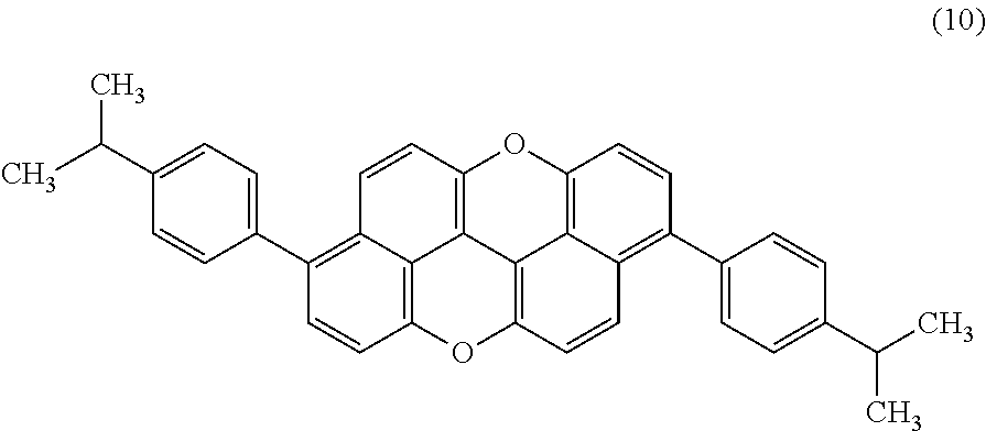
- a dioxaanthanthrene compound of Example 11 is 3,9-bis(p-isopropylphenyl)-peri-xanthenoxanthene [PXX-(iC3Ph) 2 ] represented by structural formula (10) below. That is, R 3 and R 9 are each an aryl-alkyl group.
- a dioxaanthanthrene compound of Example 11 is 3,9-bis(p-isopropylphenyl)-peri-xanthenoxanthene obtained by reacting peri-xanthenoxanthene with bromine to produce 3,9-dibromo-peri-xanthenoxanthene, and then by replacing bromine atoms with p-isopropylphenyl groups.
- PXX-(iC3Ph) 2 of Example 11 was obtained according to the same scheme as that in Example 4, except that (4,4,5,5-tetramethyl-1,3,2-dioxaborolan-2-yl)benzene was changed to p-isopropylphenylboronic acid in the synthesis process. Then, purification was performed by sublimation under high vacuum, followed by recrystallization using toluene. It was confirmed by Tof-MS and 1 H-NMR that the resulting compound was a disubstituted product, i.e., PXX-(iC3Ph) 2 .
- Example 12 also relates to dioxaanthanthrene compounds according to the first and second embodiments of the present invention, and further relates to dioxaanthanthrene compounds according to the third and twelfth embodiments.
- a dioxaanthanthrene compound of Example 12 is 3,9-bis(4-propylphenyl)-peri-xanthenoxanthene [PXX—(C3Ph) 2 ] represented by structural formula (11) below. That is, R 3 and R 9 are each an aryl-alkyl group.
- a dioxaanthanthrene compound of Example 12 is 3,9-bis(4-propylphenyl)-peri-xanthenoxanthene obtained by reacting peri-xanthenoxanthene with bromine to produce 3,9-dibromo-peri-xanthenoxanthene, and then by replacing bromine atoms with 4-propylphenyl groups.
- PXX—(C3Ph) 2 of Example 12 was obtained according to the same scheme as that in Example 4, except that (4,4,5,5-tetramethyl-1,3,2-dioxaborolan-2-yl)benzene was changed to 4-propylphenylboronic acid in the synthesis process. Then, purification was performed by sublimation under high vacuum, followed by recrystallization using toluene. It was confirmed by Tof-MS and 1 H-NMR that the resulting compound was a disubstituted product, i.e., PXX—(C3Ph) 2 .
- Example 13 also relates to dioxaanthanthrene compounds according to the first and second embodiments of the present invention, and further relates to dioxaanthanthrene compounds according to the third and thirteenth embodiments.
- a dioxaanthanthrene compound of Example 13 is 3,9-bis(4-butylphenyl)-peri-xanthenoxanthene [PXX—(C4Ph) 2 ] represented by structural formula (12) below. That is, R 3 and R 9 are each an aryl-alkyl group.
- a dioxaanthanthrene compound of Example 13 is 3,9-bis(4-butylphenyl)-peri-xanthenoxanthene obtained by reacting peri-xanthenoxanthene with bromine to produce 3,9-dibromo-peri-xanthenoxanthene, and then by replacing bromine atoms with 4-butylphenyl groups.
- PXX—(C4Ph) 2 of Example 13 was obtained according to the same scheme as that in Example 4, except that (4,4,5,5-tetramethyl-1,3,2-dioxaborolan-2-yl)benzene was changed to 4-butylphenylboronic acid in the synthesis process. Then, purification was performed by sublimation under high vacuum, followed by recrystallization using toluene. It was confirmed by Tof-MS and 1 H-NMR that the resulting compound was a disubstituted product, i.e., PXX—(C4Ph) 2 .
- Example 14 also relates to dioxaanthanthrene compounds according to the first and second embodiments of the present invention, and further relates to dioxaanthanthrene compounds according to the third and fourteenth embodiments.
- a dioxaanthanthrene compound of Example 14 is 3,9-bis(4-nonylphenyl)-peri-xanthenoxanthene [PXX—(C9Ph) 2 ] represented by structural formula (13) below. That is, R 3 and R 9 are each an aryl-alkyl group.
- a dioxaanthanthrene compound of Example 14 is 3,9-bis(4-nonylphenyl)-peri-xanthenoxanthene obtained by reacting peri-xanthenoxanthene with bromine to produce 3,9-dibromo-peri-xanthenoxanthene, and then by replacing bromine atoms with 4-nonylphenyl groups.
- PXX—(C9Ph) 2 of Example 14 was obtained according to the same scheme as that in Example 4, except that (4,4,5,5-tetramethyl-1,3,2-dioxaborolan-2-yl)benzene was changed to 4-normal-nonylbenzene boronic acid in the synthesis process. Then, purification was performed by sublimation under high vacuum, followed by recrystallization using toluene. It was confirmed by Tof-MS that the resulting compound was a disubstituted product, i.e., PXX—(C9Ph) 2 .
- Example 15 also relates to dioxaanthanthrene compounds according to the first and second embodiments of the present invention, and further relates to dioxaanthanthrene compounds according to the third and fifteenth embodiments.
- a dioxaanthanthrene compound of Example 15 is 3,9-bis(p-biphenyl)-peri-xanthenoxanthene [PXX—(BPh) 2 ] represented by structural formula (14) below. That is, R 3 and R 9 are each an aryl group.
- a dioxaanthanthrene compound of Example 15 is 3,9-bis(p-biphenyl)-peri-xanthenoxanthene obtained by reacting peri-xanthenoxanthene with bromine to produce 3,9-dibromo-peri-xanthenoxanthene, and then by replacing bromine atoms with p-biphenyl groups.
- PXX—(BPh) 2 of Example 15 was obtained according to the same scheme as that in Example 4, except that (4,4,5,5-tetramethyl-1,3,2-dioxaborolan-2-yl)benzene was changed to 4-biphenylboronic acid in the synthesis process. Then, purification was performed by sublimation under high vacuum, followed by extraction using benzene. It was confirmed by Tof-MS that the resulting compound was a disubstituted product, i.e., PXX—(BPh) 2 .
- the present invention has been described on the basis of the preferred Examples. However, the present invention is not limited to these Examples.
- the configurations and structures of the semiconductor devices, the fabrication conditions, and the fabrication methods described above are merely exemplification, and can be altered appropriately.
- monolithic integrated circuits in which many FETs are integrated on supports or supporting members may be fabricated, or the individual FETs may be separated by cutting to produce discrete components.
Landscapes
- Engineering & Computer Science (AREA)
- Manufacturing & Machinery (AREA)
- Physics & Mathematics (AREA)
- Spectroscopy & Molecular Physics (AREA)
- Chemical & Material Sciences (AREA)
- Materials Engineering (AREA)
- Thin Film Transistor (AREA)
Abstract

wherein at least one of R3 and R9 represents a substituent other than hydrogen.
Description


wherein at least one of R3 and R9 represents a substituent other than hydrogen. In addition, the dioxaanthanthrene compound represented by structural formula (1) is referred to as the “dioxaanthanthrene compound according to the first embodiment” for the sake of convenience. In other words, the dioxaanthanthrene compound according to the first embodiment is an organic semiconductor material which is obtained by replacement with a substituent other than hydrogen at least one of

wherein at least one of R1, R3, R4, R5, R7, R9, R10, and R11 represents a substituent other than hydrogen. In addition, the dioxaanthanthrene compound represented by structural formula (2) is referred to as the “dioxaanthanthrene compound according to the second embodiment” for the sake of convenience. In other words, the dioxaanthanthrene compound according to the second embodiment an organic semiconductor material which is obtained by replacement with a substituent other than hydrogen at least one of
- 1. Overall description on semiconductor devices according to first and second embodiments of the present invention, methods of manufacturing the same, and methods of forming multilayer semiconductor thin films according to first and second embodiments of the present invention
- 2. Example 1 (Semiconductor devices according to first and second embodiments of the present invention, methods of manufacturing the same, and methods of forming multilayer semiconductor thin films according to first and second embodiments of the present invention)
- 3. Example 2 (Modification of Example 1)
- 4. Example 3 (Another modification of Example 1)
- 5. Example 4 (Dioxaanthanthrene compounds according to first to fourth embodiments of the present invention)
- 6. Example 5 (Dioxaanthanthrene compounds according to first to third and fifth embodiments of the present invention)
- 7. Example 6 (Dioxaanthanthrene compounds according to first to third and sixth embodiments of the present invention)
- 8. Example 7 (Dioxaanthanthrene compounds according to first to third and seventh embodiments of the present invention)
- 9. Example 8 (Dioxaanthanthrene compounds according to first to third and eighth embodiments of the present invention)
- 10. Example 9 (Dioxaanthanthrene compounds according to first to third and ninth embodiments of the present invention)
- 11. Example 10 (Dioxaanthanthrene compounds according to first to third and tenth embodiments of the present invention)
- 12. Example 11 (Dioxaanthanthrene compounds according to first to third and eleventh embodiments of the present invention)
- 13. Example 12 (Dioxaanthanthrene compounds according to first to third and twelfth embodiments of the present invention)
- 14. Example 13 (Dioxaanthanthrene compounds according to first to third and thirteenth embodiments of the present invention)
- 15. Example 14 (Dioxaanthanthrene compounds according to first to third and fourteenth embodiments of the present invention)
- 16. Example 15 (Dioxaanthanthrene compounds according to first to third and fifteenth embodiments of the present invention), and others
- (1-1) Case where R3 is a substituent other than hydrogen, and R9 is a hydrogen atom.
- (1-2) Case where R9 is a substituent other than hydrogen, and R3 is a hydrogen atom.
- (1-3) Case where R3 and R9 are each a substituent other than hydrogen. In case (1-3), R3 and R9 may be the same substituent or different substituents.
- (2-1) Case where R1 is a substituent other than hydrogen, and R3 to R11 are each a substituent other than hydrogen or a hydrogen atom (27 cases in total).
- (2-2) Case where R3 is a substituent other than hydrogen, and R1 and R4 to R11 are each a substituent other than hydrogen or a hydrogen atom (27 cases in total).
- (2-3) Case where R4 is a substituent other than hydrogen, and R1, R3, and R5 to R11 are each a substituent other than hydrogen or a hydrogen atom (27 cases in total).
- (2-4) Case where R5 is a substituent other than hydrogen, and R1 to R4 and R7 to R11 are each a substituent other than hydrogen or a hydrogen atom (27 cases in total).
- (2-5) Case where R7 is a substituent other than hydrogen, and R1 to R5 and R9 to R11 are each a substituent other than hydrogen or a hydrogen atom (27 cases in total).
- (2-6) Case where R9 is a substituent other than hydrogen, and R1 to R7, R10, and R11 are each a substituent other than hydrogen or a hydrogen atom (27 cases in total).
- (2-7) Case where R10 is a substituent other than hydrogen, and R1 to R9 and R11 are each a substituent other than hydrogen or a hydrogen atom (27 cases in total).
- (2-8) Case where R11 is a substituent other than hydrogen, and R1 to R10 are each a substituent other than hydrogen or a hydrogen atom (27 cases in total).
- (3-1) Case where R3 is a substituent other than hydrogen, and R1 and R4 to R11 are each a substituent other than hydrogen or a hydrogen atom (27 cases in total).
- (3-2) Case where R9 is a substituent other than hydrogen, and R1 to R7, R10, and R11 are each a substituent other than hydrogen or a hydrogen atom (27 cases in total).
- (3-3) Case where R3 and R9 are each a substituent other than hydrogen, and R1, R4, R5, R7, R10, and R11 are each a substituent other than hydrogen or a hydrogen atom (26 cases in total).
- (3-4) Case where R3 is a substituent other than hydrogen, R1 is a hydrogen atom, and R4 to R11 are each a substituent other than hydrogen or a hydrogen atom (26 cases in total).
- (3-5) Case where R3 is a substituent other than hydrogen, R7 is a hydrogen atom, and R1, R4, R5, and R9 to R11 are each a substituent other than hydrogen or a hydrogen atom (26 cases in total).
- (3-6) Case where R9 is a substituent other than hydrogen, R1 is a hydrogen atom, and R3 to R7, R10, and R11 are each a substituent other than hydrogen or a hydrogen atom (26 cases in total).
- (3-7) Case where R9 is a substituent other than hydrogen, R7 is a hydrogen atom, and R1, R3 to R5, R10, and R11 are each a substituent other than hydrogen or a hydrogen atom (26 cases in total).
- (3-8) Case where R3 and R9 are each a substituent other than hydrogen, R1 is a hydrogen atom, and R4 to R7, R10, and R11 are each a substituent other than hydrogen or a hydrogen atom (25 cases in total).
- (3-9) Case where R3 and R9 are each a substituent other than hydrogen, R7 is a hydrogen atom, and R1, R4, R5, R10, and R11 are each a substituent other than hydrogen or a hydrogen atom (25 cases in total).
- (3-10) Case where R3 and R9 are each a substituent other than hydrogen, R1 and R7 are each a hydrogen atom, and R4, R5, R10, and R11 are each a substituent other than hydrogen or a hydrogen atom (24 cases in total).
ΔG m =ΔH m −T·ΔS m (A)
where ΔHm is the enthalpy variation of the system, ΔSm is the entropy variation of the system, and T is the absolute temperature.
where k is the Boltzmann constant, NT is the total number of lattice points [NT=N1+(x·N2), where N1 is the number of molecules of the low-molecular weight substance, and N2 is the number of molecules of the polymer], χ12 is the Flory χ parameter, φ1=N1/NT, φ2=x·N2/NT, and x is the number of polymer units.
(χ12·φ1·φ2)+φ1·ln(φ1)+(φ2 /x)·ln(φ2)>0 (C)


- Crystal system: Orthorhombic system
- Space group: Pccn (#56)
- Lattice constant
- a=15.920(5) Å
- b=18.508(5) Å
- c=6.930(5) Å
- V=2041.9(17) Å3
- Z=8

-
-
P 1
-
- Crystal system: Triclinic system
- Space group: P-1 (#2)
- Lattice constant
- a=8.279(2) Å
- b=18.015(5) Å
- c=4.9516(13) Å
- α=97.291(4) °
- β=103.559(4) °
- γ=98.867(4) °
- V=699.0(3) Å3
- Z=1


Claims (15)


Priority Applications (2)
| Application Number | Priority Date | Filing Date | Title |
|---|---|---|---|
| US12/848,732 US8399288B2 (en) | 2010-08-02 | 2010-08-02 | Semiconductor device, method of manufacturing the same, and method of forming multilayer semiconductor thin film |
| US13/771,846 US8546796B2 (en) | 2010-08-02 | 2013-02-20 | Semiconductor device, method of manufacturing the same, and method of forming multilayer semiconductor thin film |
Applications Claiming Priority (1)
| Application Number | Priority Date | Filing Date | Title |
|---|---|---|---|
| US12/848,732 US8399288B2 (en) | 2010-08-02 | 2010-08-02 | Semiconductor device, method of manufacturing the same, and method of forming multilayer semiconductor thin film |
Related Child Applications (1)
| Application Number | Title | Priority Date | Filing Date |
|---|---|---|---|
| US13/771,846 Division US8546796B2 (en) | 2010-08-02 | 2013-02-20 | Semiconductor device, method of manufacturing the same, and method of forming multilayer semiconductor thin film |
Publications (2)
| Publication Number | Publication Date |
|---|---|
| US20120025173A1 US20120025173A1 (en) | 2012-02-02 |
| US8399288B2 true US8399288B2 (en) | 2013-03-19 |
Family
ID=45525798
Family Applications (2)
| Application Number | Title | Priority Date | Filing Date |
|---|---|---|---|
| US12/848,732 Expired - Fee Related US8399288B2 (en) | 2010-08-02 | 2010-08-02 | Semiconductor device, method of manufacturing the same, and method of forming multilayer semiconductor thin film |
| US13/771,846 Expired - Fee Related US8546796B2 (en) | 2010-08-02 | 2013-02-20 | Semiconductor device, method of manufacturing the same, and method of forming multilayer semiconductor thin film |
Family Applications After (1)
| Application Number | Title | Priority Date | Filing Date |
|---|---|---|---|
| US13/771,846 Expired - Fee Related US8546796B2 (en) | 2010-08-02 | 2013-02-20 | Semiconductor device, method of manufacturing the same, and method of forming multilayer semiconductor thin film |
Country Status (1)
| Country | Link |
|---|---|
| US (2) | US8399288B2 (en) |
Families Citing this family (4)
| Publication number | Priority date | Publication date | Assignee | Title |
|---|---|---|---|---|
| JP5899010B2 (en) * | 2012-03-06 | 2016-04-06 | 株式会社ダイセル | ANANTHOLENE COMPOUND AND PROCESS FOR PRODUCING THE SAME |
| WO2013157421A1 (en) * | 2012-04-17 | 2013-10-24 | ソニー株式会社 | Organic semiconductor layer, electronic device, and method for producing electronic device |
| JP2014055208A (en) * | 2012-09-11 | 2014-03-27 | Sony Corp | 6,12-dioxaanthanthrene derivative, organic semiconductor element, and method for manufacturing organic semiconductor element |
| JP2014146637A (en) * | 2013-01-28 | 2014-08-14 | Sony Corp | Electronic device and method of manufacturing the same, and method of forming laminated structure |
Citations (1)
| Publication number | Priority date | Publication date | Assignee | Title |
|---|---|---|---|---|
| US6690029B1 (en) | 2001-08-24 | 2004-02-10 | University Of Kentucky Research Foundation | Substituted pentacenes and electronic devices made with substituted pentacenes |
Family Cites Families (1)
| Publication number | Priority date | Publication date | Assignee | Title |
|---|---|---|---|---|
| JP2011012001A (en) * | 2009-07-01 | 2011-01-20 | Sony Corp | Anthanthrene-based compound and semiconductor device |
-
2010
- 2010-08-02 US US12/848,732 patent/US8399288B2/en not_active Expired - Fee Related
-
2013
- 2013-02-20 US US13/771,846 patent/US8546796B2/en not_active Expired - Fee Related
Patent Citations (1)
| Publication number | Priority date | Publication date | Assignee | Title |
|---|---|---|---|---|
| US6690029B1 (en) | 2001-08-24 | 2004-02-10 | University Of Kentucky Research Foundation | Substituted pentacenes and electronic devices made with substituted pentacenes |
Non-Patent Citations (1)
| Title |
|---|
| Norihito Kobayashi, Stable peri-Xanthenoxanthene Thin Film Transistors with Efficient Carrier Injection, Jan. 12, 2009, Chem. Matr., 21, 552-556. * |
Also Published As
| Publication number | Publication date |
|---|---|
| US20120025173A1 (en) | 2012-02-02 |
| US8546796B2 (en) | 2013-10-01 |
| US20130200343A1 (en) | 2013-08-08 |
Similar Documents
| Publication | Publication Date | Title |
|---|---|---|
| US20090289248A1 (en) | Dioxaanthanthrene compound and semiconductor device | |
| US8860018B2 (en) | Anthanthrene based compound and semiconductor device | |
| JP2008513544A (en) | Carbonyl-functionalized thiophene compounds and related device structures | |
| EP1758172A1 (en) | Organic semiconductor thin film, organic semiconductor device, organic thin film transistor, and organic electro-luminescence element | |
| US8546796B2 (en) | Semiconductor device, method of manufacturing the same, and method of forming multilayer semiconductor thin film | |
| EP2767540A1 (en) | Dioxaanthanthrene-based compound, laminated structure and molding method thereof, and electronic device and production method thereof | |
| US8129497B2 (en) | Organic thin film transistor | |
| EP1710266B1 (en) | Organic semiconductor material, organic transistor, field effect transistor, switching device and thiazole compound | |
| CN100568471C (en) | Method for forming thin film of organic semiconductor material and method for manufacturing organic thin film transistor | |
| US20150108447A1 (en) | Dioxaanthanthrene compound and electronic device | |
| JP2007088224A (en) | Organic semiconductor material and organic semiconductor film using same, organic semiconductor device, and organic thin-film transistor | |
| JP6094831B2 (en) | Organic semiconductor layer, electronic device, and manufacturing method of electronic device | |
| JP5055716B2 (en) | Method for forming organic semiconductor film and method for producing organic thin film transistor | |
| JP2007059682A (en) | Organic semiconductor material, organic semiconductor film, organic semiconductor device, and organic thin film transistor | |
| JPWO2006098121A1 (en) | Organic semiconductor material, organic semiconductor film, organic semiconductor device, organic thin film transistor, and method for forming organic thin film transistor | |
| JPWO2006064776A1 (en) | Method for producing organic thin film transistor | |
| JP2007294719A (en) | Organic thin film transistor | |
| JP2013082655A (en) | Dioxaanthanthrene-based compound and electronic device | |
| JP2008124122A (en) | Organic semiconductor thin film, organic semiconductor thin film manufacturing method, and organic semiconductor element | |
| JP2004303890A (en) | Organic thin film transistor, method of forming thin film, and method of manufacturing organic thin film transistor | |
| JP2013087071A (en) | Dioxaanthanthrene-based compound and electronic device | |
| WO2006090569A1 (en) | Organic semiconductor material, organic semiconductor film, organic semiconductor device, organic thin-film transistor, field effect transistor and switching device |
Legal Events
| Date | Code | Title | Description |
|---|---|---|---|
| AS | Assignment |
Owner name: SONY CORPORATION, JAPAN Free format text: ASSIGNMENT OF ASSIGNORS INTEREST;ASSIGNORS:KOBAYASHI, NORIHITO;SASAKI, MARI;OHE, TAKAHIRO;SIGNING DATES FROM 20101028 TO 20101203;REEL/FRAME:025505/0037 |
|
| FEPP | Fee payment procedure |
Free format text: PAYOR NUMBER ASSIGNED (ORIGINAL EVENT CODE: ASPN); ENTITY STATUS OF PATENT OWNER: LARGE ENTITY |
|
| STCF | Information on status: patent grant |
Free format text: PATENTED CASE |
|
| FPAY | Fee payment |
Year of fee payment: 4 |
|
| MAFP | Maintenance fee payment |
Free format text: PAYMENT OF MAINTENANCE FEE, 8TH YEAR, LARGE ENTITY (ORIGINAL EVENT CODE: M1552); ENTITY STATUS OF PATENT OWNER: LARGE ENTITY Year of fee payment: 8 |
|
| FEPP | Fee payment procedure |
Free format text: MAINTENANCE FEE REMINDER MAILED (ORIGINAL EVENT CODE: REM.); ENTITY STATUS OF PATENT OWNER: LARGE ENTITY |
|
| LAPS | Lapse for failure to pay maintenance fees |
Free format text: PATENT EXPIRED FOR FAILURE TO PAY MAINTENANCE FEES (ORIGINAL EVENT CODE: EXP.); ENTITY STATUS OF PATENT OWNER: LARGE ENTITY |
|
| STCH | Information on status: patent discontinuation |
Free format text: PATENT EXPIRED DUE TO NONPAYMENT OF MAINTENANCE FEES UNDER 37 CFR 1.362 |
|
| FP | Lapsed due to failure to pay maintenance fee |
Effective date: 20250319 |