US8399057B2 - Ordered vertically oriented porous inorganic films produced through solution processing - Google Patents
Ordered vertically oriented porous inorganic films produced through solution processing Download PDFInfo
- Publication number
- US8399057B2 US8399057B2 US11/449,465 US44946506A US8399057B2 US 8399057 B2 US8399057 B2 US 8399057B2 US 44946506 A US44946506 A US 44946506A US 8399057 B2 US8399057 B2 US 8399057B2
- Authority
- US
- United States
- Prior art keywords
- film
- pattern
- composite
- inorganic
- pores
- Prior art date
- Legal status (The legal status is an assumption and is not a legal conclusion. Google has not performed a legal analysis and makes no representation as to the accuracy of the status listed.)
- Expired - Fee Related, expires
Links
Images


Classifications
-
- C—CHEMISTRY; METALLURGY
- C04—CEMENTS; CONCRETE; ARTIFICIAL STONE; CERAMICS; REFRACTORIES
- C04B—LIME, MAGNESIA; SLAG; CEMENTS; COMPOSITIONS THEREOF, e.g. MORTARS, CONCRETE OR LIKE BUILDING MATERIALS; ARTIFICIAL STONE; CERAMICS; REFRACTORIES; TREATMENT OF NATURAL STONE
- C04B35/00—Shaped ceramic products characterised by their composition; Ceramics compositions; Processing powders of inorganic compounds preparatory to the manufacturing of ceramic products
- C04B35/622—Forming processes; Processing powders of inorganic compounds preparatory to the manufacturing of ceramic products
- C04B35/62218—Forming processes; Processing powders of inorganic compounds preparatory to the manufacturing of ceramic products obtaining ceramic films, e.g. by using temporary supports
-
- C—CHEMISTRY; METALLURGY
- C04—CEMENTS; CONCRETE; ARTIFICIAL STONE; CERAMICS; REFRACTORIES
- C04B—LIME, MAGNESIA; SLAG; CEMENTS; COMPOSITIONS THEREOF, e.g. MORTARS, CONCRETE OR LIKE BUILDING MATERIALS; ARTIFICIAL STONE; CERAMICS; REFRACTORIES; TREATMENT OF NATURAL STONE
- C04B35/00—Shaped ceramic products characterised by their composition; Ceramics compositions; Processing powders of inorganic compounds preparatory to the manufacturing of ceramic products
- C04B35/01—Shaped ceramic products characterised by their composition; Ceramics compositions; Processing powders of inorganic compounds preparatory to the manufacturing of ceramic products based on oxide ceramics
- C04B35/14—Shaped ceramic products characterised by their composition; Ceramics compositions; Processing powders of inorganic compounds preparatory to the manufacturing of ceramic products based on oxide ceramics based on silica
-
- C—CHEMISTRY; METALLURGY
- C04—CEMENTS; CONCRETE; ARTIFICIAL STONE; CERAMICS; REFRACTORIES
- C04B—LIME, MAGNESIA; SLAG; CEMENTS; COMPOSITIONS THEREOF, e.g. MORTARS, CONCRETE OR LIKE BUILDING MATERIALS; ARTIFICIAL STONE; CERAMICS; REFRACTORIES; TREATMENT OF NATURAL STONE
- C04B35/00—Shaped ceramic products characterised by their composition; Ceramics compositions; Processing powders of inorganic compounds preparatory to the manufacturing of ceramic products
- C04B35/01—Shaped ceramic products characterised by their composition; Ceramics compositions; Processing powders of inorganic compounds preparatory to the manufacturing of ceramic products based on oxide ceramics
- C04B35/46—Shaped ceramic products characterised by their composition; Ceramics compositions; Processing powders of inorganic compounds preparatory to the manufacturing of ceramic products based on oxide ceramics based on titanium oxides or titanates
-
- C—CHEMISTRY; METALLURGY
- C04—CEMENTS; CONCRETE; ARTIFICIAL STONE; CERAMICS; REFRACTORIES
- C04B—LIME, MAGNESIA; SLAG; CEMENTS; COMPOSITIONS THEREOF, e.g. MORTARS, CONCRETE OR LIKE BUILDING MATERIALS; ARTIFICIAL STONE; CERAMICS; REFRACTORIES; TREATMENT OF NATURAL STONE
- C04B35/00—Shaped ceramic products characterised by their composition; Ceramics compositions; Processing powders of inorganic compounds preparatory to the manufacturing of ceramic products
- C04B35/622—Forming processes; Processing powders of inorganic compounds preparatory to the manufacturing of ceramic products
- C04B35/626—Preparing or treating the powders individually or as batches ; preparing or treating macroscopic reinforcing agents for ceramic products, e.g. fibres; mechanical aspects section B
- C04B35/62605—Treating the starting powders individually or as mixtures
- C04B35/62645—Thermal treatment of powders or mixtures thereof other than sintering
- C04B35/62655—Drying, e.g. freeze-drying, spray-drying, microwave or supercritical drying
-
- C—CHEMISTRY; METALLURGY
- C04—CEMENTS; CONCRETE; ARTIFICIAL STONE; CERAMICS; REFRACTORIES
- C04B—LIME, MAGNESIA; SLAG; CEMENTS; COMPOSITIONS THEREOF, e.g. MORTARS, CONCRETE OR LIKE BUILDING MATERIALS; ARTIFICIAL STONE; CERAMICS; REFRACTORIES; TREATMENT OF NATURAL STONE
- C04B35/00—Shaped ceramic products characterised by their composition; Ceramics compositions; Processing powders of inorganic compounds preparatory to the manufacturing of ceramic products
- C04B35/622—Forming processes; Processing powders of inorganic compounds preparatory to the manufacturing of ceramic products
- C04B35/626—Preparing or treating the powders individually or as batches ; preparing or treating macroscopic reinforcing agents for ceramic products, e.g. fibres; mechanical aspects section B
- C04B35/62605—Treating the starting powders individually or as mixtures
- C04B35/6269—Curing of mixtures
-
- C—CHEMISTRY; METALLURGY
- C04—CEMENTS; CONCRETE; ARTIFICIAL STONE; CERAMICS; REFRACTORIES
- C04B—LIME, MAGNESIA; SLAG; CEMENTS; COMPOSITIONS THEREOF, e.g. MORTARS, CONCRETE OR LIKE BUILDING MATERIALS; ARTIFICIAL STONE; CERAMICS; REFRACTORIES; TREATMENT OF NATURAL STONE
- C04B38/00—Porous mortars, concrete, artificial stone or ceramic ware; Preparation thereof
- C04B38/0022—Porous mortars, concrete, artificial stone or ceramic ware; Preparation thereof obtained by a chemical conversion or reaction other than those relating to the setting or hardening of cement-like material or to the formation of a sol or a gel, e.g. by carbonising or pyrolysing preformed cellular materials based on polymers, organo-metallic or organo-silicon precursors
-
- C—CHEMISTRY; METALLURGY
- C04—CEMENTS; CONCRETE; ARTIFICIAL STONE; CERAMICS; REFRACTORIES
- C04B—LIME, MAGNESIA; SLAG; CEMENTS; COMPOSITIONS THEREOF, e.g. MORTARS, CONCRETE OR LIKE BUILDING MATERIALS; ARTIFICIAL STONE; CERAMICS; REFRACTORIES; TREATMENT OF NATURAL STONE
- C04B2235/00—Aspects relating to ceramic starting mixtures or sintered ceramic products
- C04B2235/02—Composition of constituents of the starting material or of secondary phases of the final product
- C04B2235/30—Constituents and secondary phases not being of a fibrous nature
- C04B2235/44—Metal salt constituents or additives chosen for the nature of the anions, e.g. hydrides or acetylacetonate
- C04B2235/441—Alkoxides, e.g. methoxide, tert-butoxide
-
- H—ELECTRICITY
- H01—ELECTRIC ELEMENTS
- H01G—CAPACITORS; CAPACITORS, RECTIFIERS, DETECTORS, SWITCHING DEVICES OR LIGHT-SENSITIVE DEVICES, OF THE ELECTROLYTIC TYPE
- H01G9/00—Electrolytic capacitors, rectifiers, detectors, switching devices, light-sensitive or temperature-sensitive devices; Processes of their manufacture
- H01G9/20—Light-sensitive devices
- H01G9/2027—Light-sensitive devices comprising an oxide semiconductor electrode
- H01G9/2031—Light-sensitive devices comprising an oxide semiconductor electrode comprising titanium oxide, e.g. TiO2
Definitions
- the field of the invention is porous films with straight pores oriented normal to the plane of the films.
- Porous films with straight pores oriented normal to the plane of the films are a desirable geometry for a wide range of applications.
- the state of the art for producing accessible vertical pores consisted of: optical lithography, e-beam serial lithography, ion track etching, anodic alumina, aligned diblock copolymers, and various surfactant or polymer template materials including magnetic field alignment of silica mesopores.
- Bicontinuous cubic pores do not have anisotropy between the in-plane and out of plane directions, but have homogenous porosity with a component that is normal to the substrate.
- Optical lithography is limited to features above 30 nm in pitch for EUV techniques [1,2].
- E-beam lithography is a serial method. The rest are parallel processes like that described here, but each has drawbacks.
- Track etching uses ion beams of heavy, high energy ions to irradiate a sample.
- the samples are dielectrics and semi-insulating materials like kapton with no polycrystallinity; the technique is most often applied onit to polymer films.
- the preferential etching of degraded material in the path of the ion allows cylindrical column pores to be etched out of the target.
- Single pores can be 6 nm or larger and have aspect ratios in excess of 1000. While it has no order, the density of pores is controlled by exposure time and feature density can reach 1014/cm 2 [3,4]. Throughput with this technique is limited by the collimation of the ion beam because of its reliance on ion trajectory.
- Aluminum can be anodically etched to produce vertical alumina pores.
- the process produces a disordered pore structure with diameters between 6 nm and 200 nm that is thermally stable to 800° C. As a film, this process is only able to produce pores in aluminum and only on conductive substrates [5].
- Block copolymers are two or more polymers covalently bound at one point. They microphase segregate based upon the miscibility of the blocks. This can be used to produce a material with hexagonal symmetry. In order for the cylinders to be vertically aligned there are several methods that have been applied. Heating above the glass transition in the presence of an electric field allows the system to reorganize locally about a preferred axis defined by the electric field. Specially treated surfaces that have equal contact angles to both volumes of a diblock copolymer allow orientation to be defined by the thickness of the film. When the thickness is n+ 1/2 the pore to pore distance, and the polymer is heated above the glass transition temperature, frustration of the interface leads to vertical orientation of the volumes [6].
- Templated inorganic systems rely on the interaction of a templating micelle (surfactant or polymer) and a polymerizable inorganic ( FIG. 1 ). They self assemble into a matrix which is inherently ordered and can be made porous by removing the organic component. Bicontinuous cubic phases can be produced [10, 11, 12]. Once calcined, these have a 3D pore system that is open to the top and the bottom of the film. There is no orientation control and the pores are only connected through small necks between the cubic sites. Generally, templated inorganic systems have high temperature stability and a wide variety of materials are available for the matrix, from conductors to insulators. A 2-D hexagonal system produces long cylindrical pores.
- In-plane orientation can also be controlled through the substrate, but until now it has only been possible to control orientation parallel to the substrate [15].
- Ordered inorganic pore systems can be produced by self assembly using an organic polymer or surfactant template and inorganic matrix precursors as in FIG. 1 .
- hexagonal pores produced by self assembly on homogenous substrates produce horizontal pores as in FIG. 2 .
- porous films with straight pores oriented normal to the plane of the films can be simply produced through solution processing techniques, and which can be applied to any ordered nanoporous inorganic material that can be produced by polymer or surfactant templating.
- the production takes advantage of inorganic-surfactant or inorganic-polymer co-assembly and a patterned substrate.
- the patterned substrate which is also produced via solution phase self-assembly, forces vertical orientation in a hexagonal cylinder system with no practical limits in substrate size or type. This provides a route to vertically oriented inorganic pores with a pitch ranging from 3 nm to over 15 nm and pore sizes ranging from 2 nm to over 12 nm.
- the size is tuned by the choice of organic templating agents and the deposition conditions.
- the pores can be produced with or without a capping layer which can be used to seal the nanopores.
- a method for producing an inorganic film having vertically oriented pores normal to the plane of a surface of the film in which a pattern of components of contrasting hydrophobicity and hydrophilicity is formed on the film surface.
- An inorganic/organic composite is grown on the patterned surface whereby the composite can conform to the surface pattern and form vertically oriented cylinder structures, following which the composite is treated to form a pattern of pores corresponding in location to the pattern of components.
- the surface pattern components are formed by self-assembly, crosslinking, then calcining to provide a flat patterned surface, and the nanoporous layer is similarly formed by self-assembly and crosslinking to form a nanostructure composite, and calcining or other methods to selectively remove the template and generate a porous material.
- the vertically oriented pore structures are arranged in a hexagonal pattern and the surface pattern is generated by the top surface of a cubic self-assembled material with a close lattice match to the hexagonal composite.
- the ordered, vertically oriented [porous inorganic films produced by the methods of this invention are novel.
- the method can be extended to any polymer or surfactant templated system where hexagonal nanoporous materials can be produced.
- vertical pores can be produced either from silica or titania using the same method of hexagonal-on-cubic interfacial nucleation.
- FIG. 1 is a schematic representation of the self assembly of mesopore materials in accordance with prior art
- FIG. 2 is a cross-section transmission electron microscope (TEM) image of hexagonal silica in accordance with prior art
- FIG. 3 depicts a scheme for vertical pore growth in accordance with the present invention
- FIG. 4 shows a cross-section scanning electron microscope (SEM) image of cubic titania film produced in accordance with this invention, with a hexagonal interface;
- FIG. 5 shows a cross section SEM image of a film produced in accordance with this invention, with hexagonal silica pores aligned by a cubic titania porous substrate;
- FIG. 6 shows an AFM image of a film produced in accordance with this invention, with hexagonal silica pores aligned by a cubic titania porous substrate and open to the surface;
- FIG. 7 shows a SEM image of a vertically oriented silica film where the top porosity is sealed by a thin continuous silica layer
- FIG. 8 shows a cross section SEM image of a film produced in an extension of this invention with a single film that phase separates into hexagonal vertical pores and a cubic substrate;
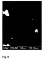
- FIG. 9 shows a cross section SEM image of a film produced in accordance with this invention, with hexagonal titania pores aligned by a cubic titania porous substrate.
- vertical pores can be produced via solution processing using a pattern of contrasting hydrophobicity, and/or hydrophilicity to direct the orientation of the liquid crystalline inorganic/organic precursor.
- the film has a pattern of hydrophobic domains or patches on a hydrophilic film surface.
- a pattern of hydrophilic domains on a hydrophobic film surface can also be used in a system based on inverse micelle self assembly.
- the pattern preferably has contrasting patches that match the hydrophobic and hydrophilic components of the final composite film.
- For aligning a composite composed of hexagonally arranged cylinders it is necessary to have a hexagonal surface pattern with a close lattice match to the composite. Since this is a surface directed orientation, roughness of the pattern must also be minimized.
- Patterns can be produced in many ways. Monolayers of nanoparticles make hexagonal patterns. Block copolymers can also be used to make a hexagonal pattern. Lithography using PDMS stamps can make a hexagonal pattern of discs [16]. While all of these methods should work, they all may have some problems, either with making very small patterns, or make highly regular patterns over large areas.
- FIG. 3 depicts a scheme for vertical pore growth in accordance with the present invention.
- the cubic pattern used must be matched to the hexagonal film system to be oriented. Production of such an oriented cubic film is compatible with deposition via spin casting, dip casting, drop casting and inkjet deposition.
- a hexagonal honeycomb structured surfactant or polymer templated inorganic/organic composite is then grown on top of the patterned surface under growth conditions where the hexagonal composite can conform to the surface pattern.
- the films can be formed under conditions where inorganic condensation proceeds slowly.
- silica pores this requires deposition from an ethanolic solution with a pH near the isoelectric point of silica ( ⁇ 2). This pH is used reduce the rate of silica condensation, thus giving the system time to rearrange into an orientation that is most compatible with the patterned substrate before the hexagonal structure is locked into place.
- Examples of specific surfactants that have been used to template the structure include Brij 58, Brij 56, or Cetyltriethylammonium bromide (CTAB). This is by no means an exhaustive list and based on reported properties, any quaternary ammonium surfactant like CTAB or any polyethylene oxide based surfactant (like the Brij series) can be used.
- Specific polymers that can be used to template the structures include Pluronics such as P123, P103, or F127 from BASF, all tri-block-copolymers with minimal capital costs.
- the di-block copolymer KLE (kraton liquid-block-polyethylene oxide) has also been shown to template these materials.
- any di- or tri-block copolymer with a polyethylene oxide (or polyethylene glycol) block can be used.
- traditional homopolymers with quaternary ammonium side change can be used to template these materials. This includes semiconducting polymers with conjugated backbones.
- a wide range of materials can be used to make the hexagonal material including almost any oxide (silica, titania, vanadia, zirconia, iron oxide, niobium oxide, tin oxide, manganese oxide, and alumina).
- Semiconducting templated materials can be produced using zintl clusters as building blocks. Systems that can be aligned include germanium, tin-germanium, silicon-germanium, platinum coupled tin tellurides, tin selenides, tin sulfides, germanium tellurides, germanium sulfides and germanium selenides. Periodic mesoporous organosilicas can be used.
- porous materials with organic groups in the walls including biphenylene, non-symmetrical 1,3-phenylene, naphthalene and terphenylene, methylene, ethane, ethylene, benzene, thiophene, acetylene, ferrocene.
- FIG. 4 which shows a cross-section SEM image of cubic titania film produced in accordance with this invention
- a substrate pattern was generated by cubic mesoporous titania and a slowly crosslinked 2D hexagonal silica film.
- the solution for the cubic titania was made using a protocol developed by Alberius et al. [17].
- 4.2 grams of tetraethylorthotitanate was mixed with 3.2 grams of concentrated HCl.
- 1 gram of Pluronic P123 dissolved in 14 grams of ethanol was added. The solution was stirred for 15 minutes and applied via dip casting at 2 cm/minute and the resulting film was aged for 4 days between ⁇ 10° C.
- the film was crosslinked by heating it first at 60° C. for 24 hours, then at 130° C. for 24 hours.
- the film was calcined with a 6 hour ramp to 350° C., held for 1 hour and a 6 hour ramp to room temperature.
- the substrate has a pattern with 15 nm pitch and appropriate hydrophobicity/hydrophilicity contrast.
- the rms roughness is under 1 nm as determined by an atomic force microscope.
- the 2D hexagonal silica was made from a protocol adapted from Stucky et al. [18].
- First 6.65 grams of Pluronic P123 and 0.8 gram of tetramethylammonium chloride was dissolved in 100 mL of ethanol.
- Second 16.65 grams of tetraethylorothosilicate and 12 grams of pH2 HCl are mixed in 50 mL of ethanol. Both solutions are stirred at 60° C. for 1 hour. They are combined and stirred for 2 hours at room temperature.
- the solution was applied by dip casting at 2 cm/min to the titania coated substrate at 50% relative humidity.
- the film was aged for 1 day at room temperature and 50% relative humidity, and hydrothermally treated for 1 day at 60° C.
- the film was calcined with a 9 hour ramp to 450° C., held for 4 hours, and cooled with a 9 hour ramp to room temperature.
- FIG. 5 shows a cross section SEM image of the end result in which a silica film was produced with 15 nm pitch and 10 nm diameter pores oriented vertically on the cubic titania substrate.
- the pores are covered in a lamellar layer.
- a slight modification of this procedure can produce pores that are open on the top so that the vertical pores can be made either sealed or unsealed.
- Example 1 produces a film with a capping layer.
- the top surface of such a film is shown in FIG. 7 .
- the tetramethylammonium chloride is left out of the synthesis. This will generate a film with slightly less straight pores, but open top porosity, as shown in FIG. 6 .
- Example 1 The procedure of Example 1 can be conducted, following which the top layer can be removed with a plasma etch to produce open pores.
- the foregoing Examples use a two step process that first involves formation of a cubic sub-film, followed by generation of a hexagonal film with vertical pore orientation using the top surface of the cubic film as a patterned nucleation site.
- the method has been extended to produce vertically oriented hexagonal pores in a single pot synthesis.
- the method works by producing a film that at the border of the cubic and hexagonal stability fields (which is controlled by the relative concentrations of the organic template and the inorganic precursor). If a composition is chosen that can not stably produce a pure hexagonal or a pure cubic phase, then multiple phases can be produced in a single film.
- Using a precursor solution that has a reagent composition chosen between the cubic and hexagonal stable regimes allows a film to be produced with both phases present.
- Spontaneous phase separation then yields a film with hexagonally packed cylinders growing from a cubic substrate similar to the two-pot synthesis where the cubic substrate is prepared separately in advance.
- the following examples illustrates one pot synthesis of vertically oriented nanoporous titania films.
- Example 4 The procedure of Example 4 was generally followed except that hexagonal titania was used instead of hexagonal silica.
- a cross section SEM image of the film so produced is shown in FIG. 9 wherein hexagonal titania pores are aligned by a cubic titania porous substrate.
- the novel use of a cubic self assembled liquid crystal system for a substrate to align a hexagonal self assembled liquid crystal system allows for features between 2 and 20 nm in size and pitch defined by choice of templating micelle agent.
- Self assembled systems offer unparalleled control over material composition and physical properties including high temperature stability and tunable electronic, catalytic, and optical properties.
- the inherent ordering of the system allows for applications like memory, which require registry and none of the brittleness associated with a lack of lattice.
- the practical limits to application area are generated only by the size of a container in dip coating, the storage area for aging, and an oven for calcination.
- the base substrate does not even need to be seriously flat as the cubic sub-phase can even out impurities.
- Capital investment is also minimal with no exotic light or ion sources.
- a wide range of applications are possible for vertically oriented nanoporous films, most of which take advantage of facile diffusion of molecules into pores of this orientation.
- the most straightforward of these applications involves separation or ultrafiltration in which solutions containing molecules or colloids are passed through a membrane made of templated vertical pores.
- Other applications take advantage of the fact that species diffused into such pores are accessible for electrical or magnetic contact from the top and bottom surfaces of the film. This opens up a very broad range of applications in electronic materials including devices such as transistors, diodes, light emitting diodes, batteries, solar cells, memory, and even logic switches.
- a wire is produced in the vertical pore by deposition or diffusion into the pores.
- Simple wires that can currently be produced in related pores systems include metals, inorganic semiconductors, and semiconducting polymers. Because of the vertical pore orientation, both top and bottom electrical contact can be made to these wires. Magnetic bits can be produced in a similar manner by filling the pores with wires made of ferrous metals or by filling the pores with stacks of magnetic nanocrystals. Importantly, because this templating method can be applied to a range of materials, applications can take advantage of both the magnetic and electronic properties of the material filling the pores and the properties of the inorganic framework itself, which can be insulating, semiconducting, or conducting
- hexagonal inorganic materials can be aligned in accordance with this invention. These materials include other oxides phases, zintl cluster based inorganic frameworks, and periodic meso porous organosilicas.
- the pores can be filled with metals, electroactive and photo active polymers, semiconductors and nanoparticles.
- the vertical pores can be used for the production of nanowire field effect transistors, nanoscale light emitting diodes, nanowire lasers, and magnetic storage based on stacked magnetic nanocrystals.
Abstract
Description
- 1. Patrick P. Naulleau. “Relevance of mask-roughness-induced printed line-edge roughness in recent and future extreme-ultraviolet lithography tests” APPLIED OPTICS 10 Jul. 2004 D Vol. 43, No. 20 D
- 2. Yang-Kyu Choi, Tsu-Jae King, and Chenming Hu. “A Spacer Patterning Technology for Nanoscale CMOS” IEEE TRANSACTIONS ON ELECTRON DEVICES, VOL. 49, NO. 3, March 2002.
- 3. M. Lindeberg, K. Hjort. “A comprehensive study of ion track enabled high aspect ratio microstructures in flexible circuit boards” Microsystem Technologies 10 (2004) 608-621.
- 4. S Metz, C Trautmann, A Bertsch and Ph Renaud. “Polyimide microfluidic devices with integrated nanoporous filtration areas manufactured by micromachining and ion track technology” J. Micromech. Microeng. 14 (2004) 324-331.
- 5. C. X. Xu, X. S. Zhang, and X. W. Sun. “Preparation of Porous Alumina by Anodization” Journal of Metastable and Nanocrystalline Materials, Vol. 23, 2005, pp. 7578.
- 6. Rachel A. Segalman. “Patterning with block copolymer thin films” Materials Science and Engineering R 48 (2005) 191-226.
- 7. Yao Lin, Alexander Boker, Jinbo He, Kevin Sill, Hongqi Xiang, Clarissa Abetz, Xuefa Li, Jin Wang, Todd Emrick, Su Long, Qian Wang, Anna Balalzs, and Thomas P. Russell. “Self directed self assembly of nanoparticle/copolymer mixtures” Nature, Vol 434, 3 Mar. 2005, pp 55-59.
- 8. Unyong Jeong, Du Yeol Ryu, Jin Kon Kim, Dong Ha Kim, Thomas P. Russell, Craig J. Hawker. “Volumen Contractions Induced by Crosslinking: A Novel Route to Nanoporous Polymer Films” Adv. Mater. 2003, 15, No. 15 pp. 1247-1250.
- 9. Miri Park, P.M. Chaikin, Richard A. Register, Douglas H. Adamson. “Large area dense nanoscale patterning of arbitrary surfaces” Applied Physics Letters —Jul. 9, 2001—Volume 79, Issue 2, pp. 257-259
- 10. David Grosso, Florence Cagno, Galo J. de A. A. Soler lilia, Eduardo L. Crepaldi, Heinz Amenitsch, Aline Brunet-Bruneau, Alexi Bourgeois, and Clement Sanchez. “Fundamentals of Mesostructuring Through Evaporation-Induced Self Assembly” Adv. Funct. Mater. 2004, 14, No. 4, April.
- 11. Ji Man Kim, Yasuhiro Sakamoto, Young Kyu Hwang, Young-Uk Kwon, Osamu Terasaki, Sang-Eon Park, Galen D. Stucky. “Structural Design of Mesoporous Silica by Micelle-Packing Control Using Blends of Amphilic Block Copolymers” J. Phys. Chem. B, 2002, 106, pp. 2552-2558.
- 12. C. J. Brinker, Yunfeng Lu, Alan Sellinger, and Hongyou Fan. “Evaporation-Induced Self-Assembly: Nanostructures Made Easy” Adv. Mater. 1999, 11, NO.7 pp579-585.
- 13. Yusuke Yamauchi, Makoto Sawada, Takashi Noma, Hidenosuke Ito, Seiichi Furumi, Yoshio Sakka, and Kazauyuki Kuroda. “Orientation of mesochannels in continuous mesoporous silica films by a high magnetic field” Journal of Materials Chemistry, 2005, 15, pp. 1137-1140.
- 14. Sarah H. Tolbert, Ali Firouzi, Galen D. Stucky, Bradley F. Chmelka. “Magnetic Field Alignment of Ordered Silicate-Surfactant Composites and Mesoporous Silica” Science, Vol 278, 1997, pp 264-268.
- 15. Hirokatsu Miyata, Kazuyuki Kuroda. “Formation of a Continous Mesoporous Silica Film with Fully Aligned Mesochannels on a Glass Substrate” Chem. Mater., 2000, 12, pp 49-54.
- 16. Rainer Pelzer, Cecile Gourgon, Stefan Landis, Paul Kettner. “Nanoimprint Lithography Full wafer Replication of Nanometer Features” Micro- and Nanotechnology: Materials, Processes, Packaging, and Systems II, February 2005, pp. 256-259.
- 17. Peter C. A. Alberius, Karen L. Frindell, Ryan C. Hayward, Edward J. Kramer, Galen D. Stucky, and Bradley Chmelka. “General Predictive Synthesis of Cubic, Hexagonal, and Lamellar Silica and Titania Mesostructured Thin Films” Chem. Mater. 2002, 14, pp. 3284-3294.
- 18. Dongjuan Zhao, Peidong Yang, Nick Melosh, Jianglin Feng, Bradley F. Chmelka, and Galen D. Stucky. “Continuous Mesoporous Silica Films with Highly Ordered Large Pore Structures” Adv. Mater. 1998, 10, No. 16, pp. 1380-1385.
Claims (20)
Priority Applications (1)
| Application Number | Priority Date | Filing Date | Title |
|---|---|---|---|
| US11/449,465 US8399057B2 (en) | 2005-06-08 | 2006-06-08 | Ordered vertically oriented porous inorganic films produced through solution processing |
Applications Claiming Priority (2)
| Application Number | Priority Date | Filing Date | Title |
|---|---|---|---|
| US68861505P | 2005-06-08 | 2005-06-08 | |
| US11/449,465 US8399057B2 (en) | 2005-06-08 | 2006-06-08 | Ordered vertically oriented porous inorganic films produced through solution processing |
Publications (2)
| Publication Number | Publication Date |
|---|---|
| US20060278158A1 US20060278158A1 (en) | 2006-12-14 |
| US8399057B2 true US8399057B2 (en) | 2013-03-19 |
Family
ID=37522975
Family Applications (1)
| Application Number | Title | Priority Date | Filing Date |
|---|---|---|---|
| US11/449,465 Expired - Fee Related US8399057B2 (en) | 2005-06-08 | 2006-06-08 | Ordered vertically oriented porous inorganic films produced through solution processing |
Country Status (1)
| Country | Link |
|---|---|
| US (1) | US8399057B2 (en) |
Families Citing this family (29)
| Publication number | Priority date | Publication date | Assignee | Title |
|---|---|---|---|---|
| JP4707995B2 (en) * | 2004-11-05 | 2011-06-22 | 富士フイルム株式会社 | Ordered nanostructured materials |
| US8394483B2 (en) * | 2007-01-24 | 2013-03-12 | Micron Technology, Inc. | Two-dimensional arrays of holes with sub-lithographic diameters formed by block copolymer self-assembly |
| US8083953B2 (en) | 2007-03-06 | 2011-12-27 | Micron Technology, Inc. | Registered structure formation via the application of directed thermal energy to diblock copolymer films |
| US8557128B2 (en) * | 2007-03-22 | 2013-10-15 | Micron Technology, Inc. | Sub-10 nm line features via rapid graphoepitaxial self-assembly of amphiphilic monolayers |
| US8097175B2 (en) | 2008-10-28 | 2012-01-17 | Micron Technology, Inc. | Method for selectively permeating a self-assembled block copolymer, method for forming metal oxide structures, method for forming a metal oxide pattern, and method for patterning a semiconductor structure |
| US8294139B2 (en) | 2007-06-21 | 2012-10-23 | Micron Technology, Inc. | Multilayer antireflection coatings, structures and devices including the same and methods of making the same |
| US7959975B2 (en) | 2007-04-18 | 2011-06-14 | Micron Technology, Inc. | Methods of patterning a substrate |
| US8372295B2 (en) | 2007-04-20 | 2013-02-12 | Micron Technology, Inc. | Extensions of self-assembled structures to increased dimensions via a “bootstrap” self-templating method |
| US8404124B2 (en) | 2007-06-12 | 2013-03-26 | Micron Technology, Inc. | Alternating self-assembling morphologies of diblock copolymers controlled by variations in surfaces |
| US8080615B2 (en) * | 2007-06-19 | 2011-12-20 | Micron Technology, Inc. | Crosslinkable graft polymer non-preferentially wetted by polystyrene and polyethylene oxide |
| US8283258B2 (en) | 2007-08-16 | 2012-10-09 | Micron Technology, Inc. | Selective wet etching of hafnium aluminum oxide films |
| US8431508B2 (en) * | 2007-10-30 | 2013-04-30 | Cerahelix, Inc. | Inorganic structure for molecular separations |
| US8999492B2 (en) | 2008-02-05 | 2015-04-07 | Micron Technology, Inc. | Method to produce nanometer-sized features with directed assembly of block copolymers |
| US8101261B2 (en) | 2008-02-13 | 2012-01-24 | Micron Technology, Inc. | One-dimensional arrays of block copolymer cylinders and applications thereof |
| US8425982B2 (en) | 2008-03-21 | 2013-04-23 | Micron Technology, Inc. | Methods of improving long range order in self-assembly of block copolymer films with ionic liquids |
| US8426313B2 (en) | 2008-03-21 | 2013-04-23 | Micron Technology, Inc. | Thermal anneal of block copolymer films with top interface constrained to wet both blocks with equal preference |
| US8114300B2 (en) | 2008-04-21 | 2012-02-14 | Micron Technology, Inc. | Multi-layer method for formation of registered arrays of cylindrical pores in polymer films |
| US8114301B2 (en) | 2008-05-02 | 2012-02-14 | Micron Technology, Inc. | Graphoepitaxial self-assembly of arrays of downward facing half-cylinders |
| WO2010056623A1 (en) * | 2008-11-11 | 2010-05-20 | Arizona Board Of Regents, A Body Corporate Of The State Of Arizona, Acting For And On Behalf Of Arizona State University | Method of making a porous polymer-metal and carbon-metal composites |
| US10472229B2 (en) | 2010-03-05 | 2019-11-12 | Cornell University—Cornell Center for Technology | Monocrystalline epitaxially aligned nanostructures and related methods |
| US8304493B2 (en) | 2010-08-20 | 2012-11-06 | Micron Technology, Inc. | Methods of forming block copolymers |
| CN102117702A (en) * | 2010-12-31 | 2011-07-06 | 上海联孚新能源科技有限公司 | Method for preparing photoanode in dye-sensitized solar cell in strong magnetic field |
| EP2517779A1 (en) * | 2011-04-26 | 2012-10-31 | Nederlandse Organisatie voor toegepast -natuurwetenschappelijk onderzoek TNO | Nanosieve composite membrane |
| US8900963B2 (en) | 2011-11-02 | 2014-12-02 | Micron Technology, Inc. | Methods of forming semiconductor device structures, and related structures |
| US9068086B2 (en) | 2011-12-21 | 2015-06-30 | Dow Global Technologies Llc | Compositions for antireflective coatings |
| US9087699B2 (en) | 2012-10-05 | 2015-07-21 | Micron Technology, Inc. | Methods of forming an array of openings in a substrate, and related methods of forming a semiconductor device structure |
| US9229328B2 (en) | 2013-05-02 | 2016-01-05 | Micron Technology, Inc. | Methods of forming semiconductor device structures, and related semiconductor device structures |
| WO2014178873A1 (en) * | 2013-05-02 | 2014-11-06 | Empire Technology Development Llc | Composition of hydrophilic painted surface |
| US9177795B2 (en) | 2013-09-27 | 2015-11-03 | Micron Technology, Inc. | Methods of forming nanostructures including metal oxides |
Citations (7)
| Publication number | Priority date | Publication date | Assignee | Title |
|---|---|---|---|---|
| US5958367A (en) * | 1995-04-03 | 1999-09-28 | Massachusetts Institute Of Technology | Methods for preparing porous metal oxides |
| US20020046682A1 (en) * | 2000-04-21 | 2002-04-25 | Hongyou Fan | Prototyping of patterned functional nanostructures |
| US20020097297A1 (en) * | 2000-12-05 | 2002-07-25 | SKINNER David | Corrision resistant hydrophobic liquid level control plate for printhead of ink jet printer and process |
| US6592764B1 (en) * | 1997-12-09 | 2003-07-15 | The Regents Of The University Of California | Block copolymer processing for mesostructured inorganic oxide materials |
| US20030157248A1 (en) * | 2001-11-21 | 2003-08-21 | Watkins James J. | Mesoporous materials and methods |
| US20040028809A1 (en) * | 2000-10-19 | 2004-02-12 | Bein Thomas W. | Porous layers and method for production thereof by means of spin-coating |
| US20060240590A1 (en) * | 2004-11-09 | 2006-10-26 | The Research Foundation Of State University Of New York | Controlled synthesis of nanowires, nanodiscs, and nanostructured materials using liquid crystalline templates |
-
2006
- 2006-06-08 US US11/449,465 patent/US8399057B2/en not_active Expired - Fee Related
Patent Citations (7)
| Publication number | Priority date | Publication date | Assignee | Title |
|---|---|---|---|---|
| US5958367A (en) * | 1995-04-03 | 1999-09-28 | Massachusetts Institute Of Technology | Methods for preparing porous metal oxides |
| US6592764B1 (en) * | 1997-12-09 | 2003-07-15 | The Regents Of The University Of California | Block copolymer processing for mesostructured inorganic oxide materials |
| US20020046682A1 (en) * | 2000-04-21 | 2002-04-25 | Hongyou Fan | Prototyping of patterned functional nanostructures |
| US20040028809A1 (en) * | 2000-10-19 | 2004-02-12 | Bein Thomas W. | Porous layers and method for production thereof by means of spin-coating |
| US20020097297A1 (en) * | 2000-12-05 | 2002-07-25 | SKINNER David | Corrision resistant hydrophobic liquid level control plate for printhead of ink jet printer and process |
| US20030157248A1 (en) * | 2001-11-21 | 2003-08-21 | Watkins James J. | Mesoporous materials and methods |
| US20060240590A1 (en) * | 2004-11-09 | 2006-10-26 | The Research Foundation Of State University Of New York | Controlled synthesis of nanowires, nanodiscs, and nanostructured materials using liquid crystalline templates |
Non-Patent Citations (18)
| Title |
|---|
| C. J. Brinker, Yunfeng Lu, Alan Sellinger, and Hongyou Fan. "Evaporation-Induced Self-Assembly: Nanostructures Made Easy" Adv. Mater. 1999, 11, No. 7 pp. 579-585. |
| C.X. Xu, X. S. Zhang, and X. W. Sun. "Preparation of Porous Alumina by Anodization" Journal of Metastable and Nanocrystalline Materials, vol. 23, 2005, pp. 7578. |
| David Grosso, Florence Cagno, Galo J. de A. A. Soler Iilia, Eduardo L. Crepaldi, Heinz Amenitsch, Aline Brunet-Bruneau, Alexi Bourgeois, and Clement Sanchez. "Fundamentals of Mesostructuring Through Evaporation-Induced Self Assembly" Adv. Funct. Mater. 2004, 14, No. 4, April. |
| Dongjuan Zhao, Peidong Yang, Nick Melosh, Jianglin Feng, Bradley F. Chmelka, and Galen Stucky. "Continuous Mesoporous Silica Films with Highly Ordered Large Pore Structures" Adv. Mater. 1998, 10, No. 16, pp. 1380-1385. |
| Hirokatsu Miyata, Kazuyuki Kuroda. "Formation of a Continous Mesoporous Silica Film with Fully Aligned Mesochannels on a Glass Substrate" Chem. Mater., 2000, 12, pp. 49-54. |
| Ji Man Kim, Yasuhiro Sakamoto, Young Kyu Hwang, Young-Uk Kwon, Osamu Terasaki, Sang-Eon Park, Galen D. Stucky. "Structural Design of Mesoporous Silica by Micelle-Packing Control Using Blends of Amphilic Block Copolymers" J. Phys. Chem. B, 2002, 106, pp. 2552-2558. |
| M. Lindeberg, K. Hjort. "A comprehensive study of ion track enabled high aspect ratio microstructures in flexible circuit boards" Microsystem Technologies 10 (2004) 608-621. |
| Miri Park, P.M. Chaikin, Richard A. Register, Douglas H. Adamson. "Large area dense nanoscale patterning of arbitrary surfaces" Applied Physics Letters-Jul. 9, 2001-vol. 79, Issue 2, pp. 257-259. |
| Patrick P. Naulleau. "Relevance of mask-roughness-induced printed line-edge roughness in recent and future extreme-ultraviolet lithography tests" Applied Optics Jul. 10, 2004 D vol. 43, No. 20. |
| Peter C. A. Alberius, Karen L. Frindell, Ryan C. Hayward, Edward J. Kramer, Galen D. Stucky, and Bradley Chmelka. "General Predictive Synthesis of Cubic, Hexagonal, and Lamellar Silica and Titania Mesostructured Thin Films" Chem. Mater. 2002, 14, pp. 3284-3294. |
| Rachel A. Segalman. "Patterning with block copolymer thin films" Materials Sdence and Engineering R 48 (2005) 191-226. |
| Rainer Pelzer, Cecile Gourgon, Stefan Landis, Paul Kettner. "Nanoimprint Lithography Full wafer Replication of Nanometer Features" Micro- and Nanotechnology: Materials, Processes, Packaging, and Systems II, Feb. 2005, pp. 256-259. |
| S Metz,C Trautmann,A Bertsch and Ph Renaud. "Polyimide microfluidic devices with integrated nanoporous filtration areas manufactured by micromachining and ion track technology" J. Micromech. Microeng. 14 (2004) 324-331. |
| Sarah H. Tolbert, Ali Firouzi, Galen D. Stucky, Bradley F. Chmelka. "Magnetic Field Alignment of Ordered Silicate-Surfactant Composites and Mesoporous Silica" Science, vol. 278, 1997, pp. 264-268. |
| Unyong Jeong, Du Yeol Ryu, Jin Kon Kim, Dong Ha Kim, Thomas P. Russell, Craig J. Hawker. "Volumen Contractions Induced by Crosslinking: A Novel Route to Nanoporous Polymer Films" Adv. Mater. 2003,15, No. 15 pp. 1247-1250. |
| Yang-Kyu Choi, Tsu-Jae King, and Chenming Hu. "A Spacer Patterning Technology for Nanoscale CMOS" IEEE Transactions on Electron Devices, vol. 49, No. 3, Mar. 2002. |
| Yao Lin, Alexander Boker, Jinbo He, Kevin Sill, Hongqi Xiang, Clarissa Abetz, Xuefa Li, Jin Wang, Todd Emrick, Su Long, Qian Wang, Anna Balalzs, and Thomas P. Russell. "Self directed self assembly of nanoparticle/copolymer mixtures" Nature, vol. 434, Mar. 3, 2005, pp. 55-59. |
| Yusuke Yamauchi, Makoto Sawada, Takashi Noma, Hidenosuke Ito, Seiichi Furumi, Yoshio Sakka, and Kazauyuki Kuroda. "Orientation of mesochannels in continuous mesoporous silica films by a high magnetic field" Journal of Materials Chemistry, 2005, 15, pp. 1137-1140. |
Also Published As
| Publication number | Publication date |
|---|---|
| US20060278158A1 (en) | 2006-12-14 |
Similar Documents
| Publication | Publication Date | Title |
|---|---|---|
| US8399057B2 (en) | Ordered vertically oriented porous inorganic films produced through solution processing | |
| Xie et al. | Review of research on template methods in preparation of nanomaterials | |
| Deng et al. | Development of solid-state nanopore fabrication technologies | |
| Brezesinski et al. | Evaporation‐Induced Self‐Assembly (EISA) at Its Limit: Ultrathin, Crystalline Patterns by Templating of Micellar Monolayers | |
| Weng et al. | Synthesis of arrayed, TiO2 needlelike nanostructures via a polystyrene-block-poly (4-vinylpyridine) diblock copolymer template | |
| Wu et al. | Electrochemical synthesis and applications of oriented and hierarchically quasi-1D semiconducting nanostructures | |
| Li et al. | Colloidal‐crystal‐assisted patterning of crystalline materials | |
| Yang et al. | Block copolymer nanopatterning for nonsemiconductor device applications | |
| Moon et al. | Can self-assembly address the permeability/selectivity trade-offs in polymer membranes? | |
| Xing et al. | Crumpled two-dimensional Ti3C2T x MXene lamellar membranes for solvent permeation and separation | |
| Ku et al. | Highly ordered freestanding titanium oxide nanotube arrays using Si-containing block copolymer lithography and atomic layer deposition | |
| Roh et al. | Understanding gas transport behavior through few-layer graphene oxide membranes controlled by tortuosity and interlayer spacing | |
| Malgras et al. | Coalescence-driven verticality in mesoporous TiO2 thin films with long-range ordering | |
| Koh et al. | Mesoporous titania thin film with highly ordered and fully accessible vertical pores and crystalline walls | |
| Wang et al. | Facile method to efficiently fabricate large-size mesoporous organosilica nanosheets with uniform tunable pore size for robust separation membranes | |
| KR101581406B1 (en) | Method of Preparing Three Dimensional Nanostructure and Three Dimensional Chiral Nanostructure | |
| KR100852628B1 (en) | Fabrication method of thin film transistor using 1 Dimensional nano-wire channel | |
| Yamauchi et al. | Fabrication of mesoporous Pt inside micrometer channels via “solvent-evaporation-mediated direct physical casting” | |
| Lee et al. | Hard templates for fabrication of nanostructured films | |
| Hur et al. | Design and Applications of Multiscale Organic–Inorganic Hybrid Materials Derived from Block Copolymer Self-Assembly | |
| Guo et al. | Soft-templating method to synthesize crystalline mesoporous α-Fe 2 O 3 films | |
| Tian et al. | Two-dimensional material membrane fabrication: progress and challenges | |
| Madkour et al. | Processing of nanomaterials (NMs) | |
| Ma et al. | High thermal stability PS-b-PEO templated mesoporous titania film | |
| JP6057278B2 (en) | POROUS MEMBRANE HAVING NETWORK METAL OXIDE SKELETON AND METHOD FOR PRODUCING THE SAME |
Legal Events
| Date | Code | Title | Description |
|---|---|---|---|
| AS | Assignment |
Owner name: CALIFORNIA, THE REGENTS OF THE UNIVERSITY OF, CALI Free format text: ASSIGNMENT OF ASSIGNORS INTEREST;ASSIGNORS:RICHMAN, ERIK K.;TOLBERT, SARAH H.;REEL/FRAME:021353/0042 Effective date: 20060711 Owner name: REGENTS OF THE UNIVERSITY OF CALIFORNIA, THE, CALI Free format text: ASSIGNMENT OF ASSIGNORS INTEREST;ASSIGNORS:RICHMAN, ERIK K.;TOLBERT, SARAH H.;REEL/FRAME:021353/0042 Effective date: 20060711 |
|
| STCF | Information on status: patent grant |
Free format text: PATENTED CASE |
|
| CC | Certificate of correction | ||
| FPAY | Fee payment |
Year of fee payment: 4 |
|
| FEPP | Fee payment procedure |
Free format text: MAINTENANCE FEE REMINDER MAILED (ORIGINAL EVENT CODE: REM.); ENTITY STATUS OF PATENT OWNER: SMALL ENTITY |
|
| LAPS | Lapse for failure to pay maintenance fees |
Free format text: PATENT EXPIRED FOR FAILURE TO PAY MAINTENANCE FEES (ORIGINAL EVENT CODE: EXP.); ENTITY STATUS OF PATENT OWNER: SMALL ENTITY |
|
| STCH | Information on status: patent discontinuation |
Free format text: PATENT EXPIRED DUE TO NONPAYMENT OF MAINTENANCE FEES UNDER 37 CFR 1.362 |
|
| FP | Lapsed due to failure to pay maintenance fee |
Effective date: 20210319 |