US8390637B2 - Method for frame memory access and display driver using the same - Google Patents
Method for frame memory access and display driver using the same Download PDFInfo
- Publication number
- US8390637B2 US8390637B2 US12/424,918 US42491809A US8390637B2 US 8390637 B2 US8390637 B2 US 8390637B2 US 42491809 A US42491809 A US 42491809A US 8390637 B2 US8390637 B2 US 8390637B2
- Authority
- US
- United States
- Prior art keywords
- row
- shift register
- memory
- pixel data
- stored
- Prior art date
- Legal status (The legal status is an assumption and is not a legal conclusion. Google has not performed a legal analysis and makes no representation as to the accuracy of the status listed.)
- Active, expires
Links
Images


Classifications
-
- G—PHYSICS
- G09—EDUCATION; CRYPTOGRAPHY; DISPLAY; ADVERTISING; SEALS
- G09G—ARRANGEMENTS OR CIRCUITS FOR CONTROL OF INDICATING DEVICES USING STATIC MEANS TO PRESENT VARIABLE INFORMATION
- G09G5/00—Control arrangements or circuits for visual indicators common to cathode-ray tube indicators and other visual indicators
- G09G5/36—Control arrangements or circuits for visual indicators common to cathode-ray tube indicators and other visual indicators characterised by the display of a graphic pattern, e.g. using an all-points-addressable [APA] memory
-
- G—PHYSICS
- G06—COMPUTING OR CALCULATING; COUNTING
- G06T—IMAGE DATA PROCESSING OR GENERATION, IN GENERAL
- G06T1/00—General purpose image data processing
- G06T1/60—Memory management
-
- G—PHYSICS
- G09—EDUCATION; CRYPTOGRAPHY; DISPLAY; ADVERTISING; SEALS
- G09G—ARRANGEMENTS OR CIRCUITS FOR CONTROL OF INDICATING DEVICES USING STATIC MEANS TO PRESENT VARIABLE INFORMATION
- G09G5/00—Control arrangements or circuits for visual indicators common to cathode-ray tube indicators and other visual indicators
- G09G5/36—Control arrangements or circuits for visual indicators common to cathode-ray tube indicators and other visual indicators characterised by the display of a graphic pattern, e.g. using an all-points-addressable [APA] memory
- G09G5/39—Control of the bit-mapped memory
- G09G5/391—Resolution modifying circuits, e.g. variable screen formats
-
- G—PHYSICS
- G09—EDUCATION; CRYPTOGRAPHY; DISPLAY; ADVERTISING; SEALS
- G09G—ARRANGEMENTS OR CIRCUITS FOR CONTROL OF INDICATING DEVICES USING STATIC MEANS TO PRESENT VARIABLE INFORMATION
- G09G5/00—Control arrangements or circuits for visual indicators common to cathode-ray tube indicators and other visual indicators
- G09G5/36—Control arrangements or circuits for visual indicators common to cathode-ray tube indicators and other visual indicators characterised by the display of a graphic pattern, e.g. using an all-points-addressable [APA] memory
- G09G5/39—Control of the bit-mapped memory
- G09G5/395—Arrangements specially adapted for transferring the contents of the bit-mapped memory to the screen
-
- G—PHYSICS
- G09—EDUCATION; CRYPTOGRAPHY; DISPLAY; ADVERTISING; SEALS
- G09G—ARRANGEMENTS OR CIRCUITS FOR CONTROL OF INDICATING DEVICES USING STATIC MEANS TO PRESENT VARIABLE INFORMATION
- G09G2340/00—Aspects of display data processing
- G09G2340/04—Changes in size, position or resolution of an image
- G09G2340/0492—Change of orientation of the displayed image, e.g. upside-down, mirrored
Definitions
- the present invention relates to the technology of a display driver, and more particularly to a memory access method for a portrait display and a landscape display, and a display driver circuit.
- one display driver integrated circuit is configured such that it can be applied to various panels.
- the panels having the same resolution of 320 ⁇ 240 Quality of Video Graphics Array, QVGA
- the challenge induced when the same integrated circuit is applied to the portrait mode and the landscape mode panels is how to effectively apply the frame memory embedded in the integrated circuit.
- the capacities of the frame memories for the portrait mode and the landscape mode are the same, but the numbers of scan lines needed in one frame and the numbers of pixels needed on each scan line in the two modes are different.
- the portrait mode QVGA panel needs 320 scan lines, and 240 pixels are needed on each scan line.
- the landscape mode QVGA panel needs 240 scan lines, and 320 pixels are needed on each scan line.
- the frame memory is configured to satisfy the requirement of the resolution of the panel. If one QVGA panel needs 320 scan lines in the portrait mode, and each scan line needs 240 pixels, then the frame memory is configured to have 320 word lines each having 240 ⁇ 24 bit lines.
- the display driver integrated circuit cannot be simultaneously applied to the landscape mode panel and the portrait mode panel.
- the present invention provides a method for frame memory access.
- the method is for storing an image with N ⁇ M pieces of pixel data to a memory with M ⁇ N storage spaces.
- the method includes the steps of: correspondingly storing the 1 st to M th pieces of pixel data of the 1 st to M th rows of the image to the 1 st to M th rows of storage spaces of the memory; and sequentially and correspondingly storing the (M+1) th to N th pieces of pixel data of the 1 st to M th rows of the image to the (M+1) th to N th rows of storage spaces of the memory.
- the method further includes the steps of: reading the data stored in the k th row of storage spaces of the memory to the 1 st to M th temporary storage positions of the shift register; shifting the (M+1) th to X th pieces of image data of the i th row of the image stored in the shift register to the (M+1) th to X th temporary storage positions of the shift register; reading the data stored in the (k+1) th row of storage spaces of the memory to the 1 st to M th temporary storage positions of the shift register; and shifting the (X+1) th to N th pieces of image data of the i th row of the image stored in
- the present invention further provides a display driving device adopted to drive a panel having N ⁇ M pixels or a panel having M ⁇ N pixels.
- the display driving device includes a memory, a shift register and a driving circuit.
- the memory has M ⁇ N storage spaces.
- the shift register has N temporary storage circuits.
- the i th temporary storage circuit is coupled to the i th column of storage spaces of the memory.
- An i th input terminal of the driving circuit is coupled to the i th temporary storage circuit of the shift register, and each of the temporary storage circuits has a corresponding temporary storage position.
- a driving stage of the display driving device includes a storing stage and a driving stage.
- the 1 st to M th pieces of pixel data of the 1 st to M th rows of an image having N ⁇ M pieces of pixel data are correspondingly stored to the 1 st to M th rows of storage spaces of the memory; and the (M+1) th to N th pieces of pixel data of the 1 st to M th rows of the image are sequentially and correspondingly stored to the (M+1) th to N th rows of storage spaces of the memory.
- the present invention mainly provides a data moving method of enabling the display driver integrated circuit with the built-in portrait style frame memory to be applied to the landscape mode.
- the spirit of this method is to repeatedly read the data from the portrait style frame memory and write the data to the shift register, to move the data over the shift register, and to put the data to the correct data latch so as to constitute the complete scan line data, and to transfer the complete scan line data to the pixel driving circuit.
- the portrait style display driver integrated circuit can drive the landscape mode display panel.
- FIG. 1 is a circuit block diagram showing a display driving device according to an embodiment of the present invention.
- FIG. 2A shows the configuration of a frame memory 102 according to the embodiment of the present invention.
- FIG. 2B is a schematic illustration showing how the frame memory 102 according to the embodiment of the present invention stores the image with the resolution of 320 ⁇ 240 in a landscape mode.
- FIGS. 3A to 3D are schematic illustrations showing how the embodiment of the present invention reads the image, which has the resolution of 320 ⁇ 240 in the landscape mode and is stored in the frame memory 102 .
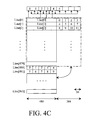
- FIGS. 4A to 4F are schematic illustrations showing how the embodiment of the present invention reads the image, which has the resolution of 864 ⁇ 480 in the landscape mode and is stored in the frame memory 102 .
- the frame memory of the display driver circuit of the present invention is the portrait display frame memory.
- a QVGA panel will be described, wherein the frame memory has 320 word lines each having 240 ⁇ 24 bit lines.
- FIG. 1 is a circuit block diagram showing a display driving device according to an embodiment of the present invention.
- the display driving device includes a driving circuit 101 , a memory 102 and a shift register 103 .
- the driving circuit 101 includes multiple digital-to-analog converters DA[01] to DA[80], multiple multiplexers mux[01] to mux[80] and multiple data latches L[01] to L[80].
- the shift register 103 includes multiple temporary storage circuits. If one temporary storage circuit stores one pixel, each temporary storage circuit needs to store three sub-pixels in total. Because each sub-pixel has 8 bits, each temporary storage circuit has 3 ⁇ 8 bits.
- the temporary storage circuit of the shift register in this embodiment is divided into 80 groups S[01] to S[80] each having 12 ⁇ 8 bits.
- the pixel driving circuit of the resolution of 240 ⁇ 320 is adopted in the pixel driving circuit of the display driving circuit 101 .
- the configuration of the 12:1 source driver is illustrated as an example.
- 80 channels DA[01] to DA[80] are needed.
- the memory 102 of this embodiment is a portrait style frame memory.
- the frame memory 102 has 320 word lines respectively corresponding to 320 scan lines. Each word line has 240 ⁇ 24 bit lines respectively corresponding to 240 ⁇ 3 (R, G, B) pixels.
- the shift register 103 is added in this embodiment, and the total storage spaces of the shift register 103 are 320 ⁇ 24 bits (320 ⁇ 3 sub-pixels each needing 8 bits).
- the 1 st to 60 th channels DA[01] to DA[60] correspond to 240 pixels and each column of the frame memory 102 .
- additional 20 channels DA[61] to DA[80] are needed to correspond to the display requirements of the 241 st to 320 th pixels.
- FIG. 2A shows the configuration of the frame memory 102 according to the embodiment of the present invention.
- FIG. 2B is a schematic illustration showing how the frame memory 102 according to the embodiment of the present invention stores the image with the resolution of 320 ⁇ 240 in the landscape mode.
- the data sizes of the image of the resolution of 320 ⁇ 240 and the image of the resolution of 240 ⁇ 320 are substantially the same.
- the frame memory 102 can absolutely store the data. However, if the data are stored arbitrarily, the data cannot be easily taken out and may cause the poor efficiency of the circuit operation.
- the method of storing the image data in the frame memory 102 is to store the first 240 pixels of each row to the corresponding storage positions of each row of the frame memory 102 . That is, the first 240 pixels of the i th row of the image data are stored in the i th row of the frame memory 102 . At this time, each row of the image data still has 80 pixels that have not been stored yet. Next, the remaining 80 pixels of each row of the image data are sequentially stored to the 241 st to 320 th rows (Line[239] to Line[319]) of the frame memory 102 . This purposes and advantages of this storing method will be described in the following embodiments.
- FIGS. 3A to 3D are schematic illustrations showing how the embodiment of the present invention reads the image, which has the resolution of 320 ⁇ 240 in the landscape mode and is stored in the frame memory 102 .
- the shift register 103 is divided into four blocks 301 to 304 , and the data in the blocks 301 to 303 may be respectively shifted to the block 304 .
- FIG. 3B if the data on the first scan line is to be taken out, the data on Line[240] will be taken out first and temporarily stored to the blocks 301 to 303 of the shift register 103 .
- FIG. 3B if the data on the first scan line is to be taken out, the data on Line[240] will be taken out first and temporarily stored to the blocks 301 to 303 of the shift register 103 .
- the driving circuit 101 can drive the landscape mode display panel according to its predetermined driving operation procedure.
- FIGS. 4A to 4F are schematic illustrations showing how the embodiment of the present invention reads the image, which has the resolution of 864 ⁇ 480 in the landscape mode and is stored in the frame memory 102 .
- the landscape mode corresponds to 864 ⁇ 480
- the frame memory 102 of this embodiment is used in conjunction with the resolution of 480 ⁇ 864.
- the shift register 103 in this embodiment is divided into nine blocks 401 to 409 , and the data in the blocks 401 to 405 may be respectively moved to the blocks 406 to 409 .
- the driving circuit 101 may drive the landscape mode display panel according to its predetermined driving operation procedure.
- the present invention mainly provides a data moving method of enabling the display driver integrated circuit with the built-in portrait style frame memory to be applied to the landscape mode.
- the spirit of this method is to repeatedly read the data from the portrait style frame memory and write the data to the shift register, to move the data over the shift register, and to put the data to the correct data latch so as to constitute the complete scan line data, and to transfer the complete scan line data to the pixel driving circuit.
- the portrait style display driver integrated circuit can drive the landscape mode display panel.
Landscapes
- Engineering & Computer Science (AREA)
- Physics & Mathematics (AREA)
- General Physics & Mathematics (AREA)
- Theoretical Computer Science (AREA)
- Computer Hardware Design (AREA)
- Control Of Indicators Other Than Cathode Ray Tubes (AREA)
- Controls And Circuits For Display Device (AREA)
- Liquid Crystal Display Device Control (AREA)
- Liquid Crystal (AREA)
Abstract
Description
Claims (2)
Applications Claiming Priority (3)
| Application Number | Priority Date | Filing Date | Title |
|---|---|---|---|
| TW097143986 | 2008-11-14 | ||
| TW97143986A | 2008-11-14 | ||
| TW097143986A TWI391912B (en) | 2008-11-14 | 2008-11-14 | Frame memory access method and display driver using the same |
Publications (2)
| Publication Number | Publication Date |
|---|---|
| US20100123730A1 US20100123730A1 (en) | 2010-05-20 |
| US8390637B2 true US8390637B2 (en) | 2013-03-05 |
Family
ID=42171668
Family Applications (1)
| Application Number | Title | Priority Date | Filing Date |
|---|---|---|---|
| US12/424,918 Active 2031-12-29 US8390637B2 (en) | 2008-11-14 | 2009-04-16 | Method for frame memory access and display driver using the same |
Country Status (3)
| Country | Link |
|---|---|
| US (1) | US8390637B2 (en) |
| JP (1) | JP5031002B2 (en) |
| TW (1) | TWI391912B (en) |
Families Citing this family (1)
| Publication number | Priority date | Publication date | Assignee | Title |
|---|---|---|---|---|
| JP2020076863A (en) * | 2018-11-07 | 2020-05-21 | キヤノン株式会社 | Display device and electronic equipment |
Citations (3)
| Publication number | Priority date | Publication date | Assignee | Title |
|---|---|---|---|---|
| US4546451A (en) * | 1982-02-12 | 1985-10-08 | Metheus Corporation | Raster graphics display refresh memory architecture offering rapid access speed |
| US6400851B1 (en) * | 1999-01-28 | 2002-06-04 | Microsoft Corporation | Rotating image data |
| US20060284904A1 (en) * | 2005-06-16 | 2006-12-21 | Ng Sunny Y | System and method for using current pixel voltages to drive display |
Family Cites Families (4)
| Publication number | Priority date | Publication date | Assignee | Title |
|---|---|---|---|---|
| JPH05334426A (en) * | 1992-06-04 | 1993-12-17 | Anritsu Corp | Image data storage |
| JPH1138957A (en) * | 1997-07-22 | 1999-02-12 | Toshiba Corp | Image data VRAM mapping method and image display system |
| TWI242741B (en) * | 2004-05-10 | 2005-11-01 | Faraday Tech Corp | Method for accessing frame data and data accessing device thereof |
| US20060127059A1 (en) * | 2004-12-14 | 2006-06-15 | Blaise Fanning | Media player with high-resolution and low-resolution image frame buffers |
-
2008
- 2008-11-14 TW TW097143986A patent/TWI391912B/en not_active IP Right Cessation
-
2009
- 2009-04-16 US US12/424,918 patent/US8390637B2/en active Active
- 2009-07-09 JP JP2009163188A patent/JP5031002B2/en active Active
Patent Citations (3)
| Publication number | Priority date | Publication date | Assignee | Title |
|---|---|---|---|---|
| US4546451A (en) * | 1982-02-12 | 1985-10-08 | Metheus Corporation | Raster graphics display refresh memory architecture offering rapid access speed |
| US6400851B1 (en) * | 1999-01-28 | 2002-06-04 | Microsoft Corporation | Rotating image data |
| US20060284904A1 (en) * | 2005-06-16 | 2006-12-21 | Ng Sunny Y | System and method for using current pixel voltages to drive display |
Also Published As
| Publication number | Publication date |
|---|---|
| JP5031002B2 (en) | 2012-09-19 |
| TW201019313A (en) | 2010-05-16 |
| TWI391912B (en) | 2013-04-01 |
| US20100123730A1 (en) | 2010-05-20 |
| JP2010117704A (en) | 2010-05-27 |
Similar Documents
| Publication | Publication Date | Title |
|---|---|---|
| US12183240B2 (en) | Display panel and display device | |
| US7859928B2 (en) | Integrated circuit device and electronic instrument | |
| US7782694B2 (en) | Integrated circuit device and electronic instrument | |
| US7613066B2 (en) | Integrated circuit device and electronic instrument | |
| US7411861B2 (en) | Integrated circuit device and electronic instrument | |
| US20080112254A1 (en) | Integrated circuit device and electronic instrument | |
| US20070013706A1 (en) | Integrated circuit device and electronic instrument | |
| US20060232541A1 (en) | Display device and method for driving a display device | |
| US20070035503A1 (en) | Display driver control circuit and electronic equipment with display device | |
| US7593270B2 (en) | Integrated circuit device and electronic instrument | |
| US7616520B2 (en) | Integrated circuit device and electronic instrument | |
| US7986541B2 (en) | Integrated circuit device and electronic instrument | |
| US20070001968A1 (en) | Display device and electronic instrument | |
| US20070001970A1 (en) | Integrated circuit device and electronic instrument | |
| US11875753B2 (en) | Data driver and display device including a data driver | |
| US8390637B2 (en) | Method for frame memory access and display driver using the same | |
| US20090015604A1 (en) | Display device and electronic device using the same | |
| US8723878B2 (en) | Display device integrated circuit (DDI) with adaptive memory control and adaptive memory control method for DDI | |
| US8947445B2 (en) | Display controller and display device including the same | |
| US20070002060A1 (en) | Virtual device buffer for embedded device | |
| CN101751908A (en) | Frame memory access method and display driving device | |
| US7177202B2 (en) | Method for accessing a single port memory | |
| US7492370B2 (en) | Management method and display method of on-screen display thereof and related display controlling device | |
| US12230183B2 (en) | Display device | |
| KR102537301B1 (en) | Display device and a method of driving the same |
Legal Events
| Date | Code | Title | Description |
|---|---|---|---|
| AS | Assignment |
Owner name: ORISE TECHNOLOGY CO., LTD.,TAIWAN Free format text: ASSIGNMENT OF ASSIGNORS INTEREST;ASSIGNORS:WANG, SZU-MIEN;YANG, DAN-CHI;HUANG, SHIH CHUAN;REEL/FRAME:022556/0704 Effective date: 20090320 Owner name: ORISE TECHNOLOGY CO., LTD., TAIWAN Free format text: ASSIGNMENT OF ASSIGNORS INTEREST;ASSIGNORS:WANG, SZU-MIEN;YANG, DAN-CHI;HUANG, SHIH CHUAN;REEL/FRAME:022556/0704 Effective date: 20090320 |
|
| STCF | Information on status: patent grant |
Free format text: PATENTED CASE |
|
| FPAY | Fee payment |
Year of fee payment: 4 |
|
| MAFP | Maintenance fee payment |
Free format text: PAYMENT OF MAINTENANCE FEE, 8TH YR, SMALL ENTITY (ORIGINAL EVENT CODE: M2552); ENTITY STATUS OF PATENT OWNER: SMALL ENTITY Year of fee payment: 8 |
|
| MAFP | Maintenance fee payment |
Free format text: PAYMENT OF MAINTENANCE FEE, 12TH YR, SMALL ENTITY (ORIGINAL EVENT CODE: M2553); ENTITY STATUS OF PATENT OWNER: SMALL ENTITY Year of fee payment: 12 |