US8372526B2 - Intermediate connector for stacked organic light emitting devices - Google Patents
Intermediate connector for stacked organic light emitting devices Download PDFInfo
- Publication number
- US8372526B2 US8372526B2 US12/174,286 US17428608A US8372526B2 US 8372526 B2 US8372526 B2 US 8372526B2 US 17428608 A US17428608 A US 17428608A US 8372526 B2 US8372526 B2 US 8372526B2
- Authority
- US
- United States
- Prior art keywords
- layer
- metal
- substituted
- unsubstituted
- organic
- Prior art date
- Legal status (The legal status is an assumption and is not a legal conclusion. Google has not performed a legal analysis and makes no representation as to the accuracy of the status listed.)
- Active, expires
Links
- 239000000463 material Substances 0.000 claims abstract description 132
- 229910052751 metal Inorganic materials 0.000 claims abstract description 126
- 239000002184 metal Substances 0.000 claims abstract description 126
- 239000012044 organic layer Substances 0.000 claims abstract description 81
- 239000010410 layer Substances 0.000 claims description 162
- 125000003118 aryl group Chemical group 0.000 claims description 28
- 125000000623 heterocyclic group Chemical group 0.000 claims description 12
- 229910044991 metal oxide Inorganic materials 0.000 claims description 11
- 150000004706 metal oxides Chemical class 0.000 claims description 11
- 229910001507 metal halide Inorganic materials 0.000 claims description 10
- 150000005309 metal halides Chemical class 0.000 claims description 10
- 150000004982 aromatic amines Chemical class 0.000 claims description 9
- 125000001424 substituent group Chemical group 0.000 claims description 9
- 125000006743 (C1-C60) alkyl group Chemical group 0.000 claims description 8
- 150000001408 amides Chemical class 0.000 claims description 8
- ZUOUZKKEUPVFJK-UHFFFAOYSA-N diphenyl Chemical compound C1=CC=CC=C1C1=CC=CC=C1 ZUOUZKKEUPVFJK-UHFFFAOYSA-N 0.000 claims description 8
- 125000002023 trifluoromethyl group Chemical group FC(F)(F)* 0.000 claims description 8
- RTZKZFJDLAIYFH-UHFFFAOYSA-N Diethyl ether Chemical compound CCOCC RTZKZFJDLAIYFH-UHFFFAOYSA-N 0.000 claims description 6
- 125000001475 halogen functional group Chemical group 0.000 claims description 5
- 238000001429 visible spectrum Methods 0.000 claims description 5
- 125000004642 (C1-C12) alkoxy group Chemical group 0.000 claims description 4
- 125000004400 (C1-C12) alkyl group Chemical group 0.000 claims description 4
- YJTKZCDBKVTVBY-UHFFFAOYSA-N 1,3-Diphenylbenzene Chemical group C1=CC=CC=C1C1=CC=CC(C=2C=CC=CC=2)=C1 YJTKZCDBKVTVBY-UHFFFAOYSA-N 0.000 claims description 4
- JCXJVPUVTGWSNB-UHFFFAOYSA-N Nitrogen dioxide Chemical compound O=[N]=O JCXJVPUVTGWSNB-UHFFFAOYSA-N 0.000 claims description 4
- 150000001412 amines Chemical class 0.000 claims description 4
- 125000002178 anthracenyl group Chemical group C1(=CC=CC2=CC3=CC=CC=C3C=C12)* 0.000 claims description 4
- 235000010290 biphenyl Nutrition 0.000 claims description 4
- 239000004305 biphenyl Substances 0.000 claims description 4
- 125000003336 coronenyl group Chemical group C1(=CC2=CC=C3C=CC4=CC=C5C=CC6=CC=C1C1=C6C5=C4C3=C21)* 0.000 claims description 4
- 125000004185 ester group Chemical group 0.000 claims description 4
- 150000002148 esters Chemical class 0.000 claims description 4
- 229910052739 hydrogen Inorganic materials 0.000 claims description 4
- 239000001257 hydrogen Substances 0.000 claims description 4
- 125000004435 hydrogen atom Chemical class [H]* 0.000 claims description 4
- 125000001624 naphthyl group Chemical group 0.000 claims description 4
- 150000002825 nitriles Chemical class 0.000 claims description 4
- 125000000449 nitro group Chemical group [O-][N+](*)=O 0.000 claims description 4
- 125000003933 pentacenyl group Chemical group C1(=CC=CC2=CC3=CC4=CC5=CC=CC=C5C=C4C=C3C=C12)* 0.000 claims description 4
- 125000002080 perylenyl group Chemical group C1(=CC=C2C=CC=C3C4=CC=CC5=CC=CC(C1=C23)=C45)* 0.000 claims description 4
- 125000001997 phenyl group Chemical group [H]C1=C([H])C([H])=C(*)C([H])=C1[H] 0.000 claims description 4
- 229940124530 sulfonamide Drugs 0.000 claims description 4
- 150000003456 sulfonamides Chemical class 0.000 claims description 4
- BDHFUVZGWQCTTF-UHFFFAOYSA-M sulfonate Chemical compound [O-]S(=O)=O BDHFUVZGWQCTTF-UHFFFAOYSA-M 0.000 claims description 4
- 125000000472 sulfonyl group Chemical group *S(*)(=O)=O 0.000 claims description 4
- 150000003462 sulfoxides Chemical class 0.000 claims description 4
- 125000001935 tetracenyl group Chemical group C1(=CC=CC2=CC3=CC4=CC=CC=C4C=C3C=C12)* 0.000 claims description 4
- 150000002739 metals Chemical class 0.000 description 21
- 239000011368 organic material Substances 0.000 description 21
- 239000007924 injection Substances 0.000 description 17
- 238000002347 injection Methods 0.000 description 17
- 239000002019 doping agent Substances 0.000 description 13
- 150000003384 small molecules Chemical class 0.000 description 12
- 239000000758 substrate Substances 0.000 description 12
- 150000001875 compounds Chemical class 0.000 description 10
- 238000004770 highest occupied molecular orbital Methods 0.000 description 10
- 238000004768 lowest unoccupied molecular orbital Methods 0.000 description 9
- 238000000034 method Methods 0.000 description 8
- 0 [1*]C1=C([2*])N=C2C(=N1)C1=C(N=C([5*])C([6*])=N1)C1=C2N=C([3*])C([4*])=N1 Chemical compound [1*]C1=C([2*])N=C2C(=N1)C1=C(N=C([5*])C([6*])=N1)C1=C2N=C([3*])C([4*])=N1 0.000 description 7
- 230000000903 blocking effect Effects 0.000 description 7
- 238000000151 deposition Methods 0.000 description 7
- DHDHJYNTEFLIHY-UHFFFAOYSA-N 4,7-diphenyl-1,10-phenanthroline Chemical group C1=CC=CC=C1C1=CC=NC2=C1C=CC1=C(C=3C=CC=CC=3)C=CN=C21 DHDHJYNTEFLIHY-UHFFFAOYSA-N 0.000 description 6
- RAXXELZNTBOGNW-UHFFFAOYSA-N imidazole Natural products C1=CNC=N1 RAXXELZNTBOGNW-UHFFFAOYSA-N 0.000 description 6
- 239000003446 ligand Substances 0.000 description 6
- 229920000642 polymer Polymers 0.000 description 6
- 230000032258 transport Effects 0.000 description 6
- 239000000412 dendrimer Substances 0.000 description 5
- 229920000736 dendritic polymer Polymers 0.000 description 5
- 230000000694 effects Effects 0.000 description 5
- 230000005525 hole transport Effects 0.000 description 5
- 238000004519 manufacturing process Methods 0.000 description 5
- 230000005693 optoelectronics Effects 0.000 description 5
- 239000000243 solution Substances 0.000 description 5
- IJGRMHOSHXDMSA-UHFFFAOYSA-N Atomic nitrogen Chemical compound N#N IJGRMHOSHXDMSA-UHFFFAOYSA-N 0.000 description 4
- UFVXQDWNSAGPHN-UHFFFAOYSA-K bis[(2-methylquinolin-8-yl)oxy]-(4-phenylphenoxy)alumane Chemical compound [Al+3].C1=CC=C([O-])C2=NC(C)=CC=C21.C1=CC=C([O-])C2=NC(C)=CC=C21.C1=CC([O-])=CC=C1C1=CC=CC=C1 UFVXQDWNSAGPHN-UHFFFAOYSA-K 0.000 description 4
- 238000010586 diagram Methods 0.000 description 4
- IBHBKWKFFTZAHE-UHFFFAOYSA-N n-[4-[4-(n-naphthalen-1-ylanilino)phenyl]phenyl]-n-phenylnaphthalen-1-amine Chemical compound C1=CC=CC=C1N(C=1C2=CC=CC=C2C=CC=1)C1=CC=C(C=2C=CC(=CC=2)N(C=2C=CC=CC=2)C=2C3=CC=CC=C3C=CC=2)C=C1 IBHBKWKFFTZAHE-UHFFFAOYSA-N 0.000 description 4
- 229910052709 silver Inorganic materials 0.000 description 4
- UHBIKXOBLZWFKM-UHFFFAOYSA-N 8-hydroxy-2-quinolinecarboxylic acid Chemical class C1=CC=C(O)C2=NC(C(=O)O)=CC=C21 UHBIKXOBLZWFKM-UHFFFAOYSA-N 0.000 description 3
- VFUDMQLBKNMONU-UHFFFAOYSA-N C1=CC2=C(C=C1)N(C1=CC=C(C3=CC=C(N4C5=C(C=CC=C5)C5=C4C=CC=C5)C=C3)C=C1)C1=C2C=CC=C1 Chemical compound C1=CC2=C(C=C1)N(C1=CC=C(C3=CC=C(N4C5=C(C=CC=C5)C5=C4C=CC=C5)C=C3)C=C1)C1=C2C=CC=C1 VFUDMQLBKNMONU-UHFFFAOYSA-N 0.000 description 3
- GEQBRULPNIVQPP-UHFFFAOYSA-N C1=CC=C(N2C(C3=CC(C4=NC5=C(C=CC=C5)N4C4=CC=CC=C4)=CC(/C4=N/C5=C(C=CC=C5)N4C4=CC=CC=C4)=C3)=NC3=C2C=CC=C3)C=C1 Chemical compound C1=CC=C(N2C(C3=CC(C4=NC5=C(C=CC=C5)N4C4=CC=CC=C4)=CC(/C4=N/C5=C(C=CC=C5)N4C4=CC=CC=C4)=C3)=NC3=C2C=CC=C3)C=C1 GEQBRULPNIVQPP-UHFFFAOYSA-N 0.000 description 3
- STTGYIUESPWXOW-UHFFFAOYSA-N CC1=NC2=C(C=CC3=C2N=C(C)C=C3C2=CC=CC=C2)C(C2=CC=CC=C2)=C1 Chemical compound CC1=NC2=C(C=CC3=C2N=C(C)C=C3C2=CC=CC=C2)C(C2=CC=CC=C2)=C1 STTGYIUESPWXOW-UHFFFAOYSA-N 0.000 description 3
- 125000000217 alkyl group Chemical group 0.000 description 3
- 229910052782 aluminium Inorganic materials 0.000 description 3
- 230000008901 benefit Effects 0.000 description 3
- 239000003086 colorant Substances 0.000 description 3
- 230000002950 deficient Effects 0.000 description 3
- 229910052749 magnesium Inorganic materials 0.000 description 3
- 230000007246 mechanism Effects 0.000 description 3
- 239000000203 mixture Substances 0.000 description 3
- WCPAKWJPBJAGKN-UHFFFAOYSA-N oxadiazole Chemical compound C1=CON=N1 WCPAKWJPBJAGKN-UHFFFAOYSA-N 0.000 description 3
- 150000003852 triazoles Chemical class 0.000 description 3
- HYZJCKYKOHLVJF-UHFFFAOYSA-N 1H-benzimidazole Chemical compound C1=CC=C2NC=NC2=C1 HYZJCKYKOHLVJF-UHFFFAOYSA-N 0.000 description 2
- HIXDQWDOVZUNNA-UHFFFAOYSA-N 2-(3,4-dimethoxyphenyl)-5-hydroxy-7-methoxychromen-4-one Chemical compound C=1C(OC)=CC(O)=C(C(C=2)=O)C=1OC=2C1=CC=C(OC)C(OC)=C1 HIXDQWDOVZUNNA-UHFFFAOYSA-N 0.000 description 2
- NSXJEEMTGWMJPY-UHFFFAOYSA-N C1=CC(N2C3=C(C=CC=C3)C3=C2C=CC=C3)=CC(C2=CC=CC(N3C4=C(C=CC=C4)C4=C3/C=C\C=C/4)=C2)=C1 Chemical compound C1=CC(N2C3=C(C=CC=C3)C3=C2C=CC=C3)=CC(C2=CC=CC(N3C4=C(C=CC=C4)C4=C3/C=C\C=C/4)=C2)=C1 NSXJEEMTGWMJPY-UHFFFAOYSA-N 0.000 description 2
- MZYDBGLUVPLRKR-UHFFFAOYSA-N C1=CC(N2C3=C(C=CC=C3)C3=C2C=CC=C3)=CC(N2C3=C(C=CC=C3)C3=C2C=CC=C3)=C1 Chemical compound C1=CC(N2C3=C(C=CC=C3)C3=C2C=CC=C3)=CC(N2C3=C(C=CC=C3)C3=C2C=CC=C3)=C1 MZYDBGLUVPLRKR-UHFFFAOYSA-N 0.000 description 2
- SDEFDICGRVDKPH-UHFFFAOYSA-M C1=CC2=C3C(=C1)O[AlH]N3=CC=C2 Chemical compound C1=CC2=C3C(=C1)O[AlH]N3=CC=C2 SDEFDICGRVDKPH-UHFFFAOYSA-M 0.000 description 2
- RSWOJEDGRFCGFR-UHFFFAOYSA-N C1=CC=C(C2=CC3=C(C=C2C2=CC=CC=C2)C2=C(C=C(C4=CC=CC=C4)C(C4=CC=CC=C4)=C2)C2=CC(C4=CC=CC=C4)=C(C4=CC=CC=C4)C=C23)C=C1 Chemical compound C1=CC=C(C2=CC3=C(C=C2C2=CC=CC=C2)C2=C(C=C(C4=CC=CC=C4)C(C4=CC=CC=C4)=C2)C2=CC(C4=CC=CC=C4)=C(C4=CC=CC=C4)C=C23)C=C1 RSWOJEDGRFCGFR-UHFFFAOYSA-N 0.000 description 2
- XYYYIVRDTLXJEF-UHFFFAOYSA-L CC1=N2C3=C(C=CC=C3O[Al]2OC2=CC=C(C3=CC=CC=C3)C=C2)C=C1 Chemical compound CC1=N2C3=C(C=CC=C3O[Al]2OC2=CC=C(C3=CC=CC=C3)C=C2)C=C1 XYYYIVRDTLXJEF-UHFFFAOYSA-L 0.000 description 2
- OGQNNUOGXDHJDW-UHFFFAOYSA-N [C-]#[N+]C1=NC2=C(N=C1[N+]#[C-])C1=C(N=C(C#N)C(C#N)=N1)C1=NC(C#N)=C([N+]#[C-])N=C12 Chemical compound [C-]#[N+]C1=NC2=C(N=C1[N+]#[C-])C1=C(N=C(C#N)C(C#N)=N1)C1=NC(C#N)=C([N+]#[C-])N=C12 OGQNNUOGXDHJDW-UHFFFAOYSA-N 0.000 description 2
- 230000002411 adverse Effects 0.000 description 2
- -1 arylkyl Chemical group 0.000 description 2
- 238000005452 bending Methods 0.000 description 2
- 230000008021 deposition Effects 0.000 description 2
- 230000002349 favourable effect Effects 0.000 description 2
- 238000005286 illumination Methods 0.000 description 2
- 239000012535 impurity Substances 0.000 description 2
- UEEXRMUCXBPYOV-UHFFFAOYSA-N iridium;2-phenylpyridine Chemical group [Ir].C1=CC=CC=C1C1=CC=CC=N1.C1=CC=CC=C1C1=CC=CC=N1.C1=CC=CC=C1C1=CC=CC=N1 UEEXRMUCXBPYOV-UHFFFAOYSA-N 0.000 description 2
- 239000011159 matrix material Substances 0.000 description 2
- 229910052757 nitrogen Inorganic materials 0.000 description 2
- 230000003287 optical effect Effects 0.000 description 2
- 125000002524 organometallic group Chemical group 0.000 description 2
- 238000000059 patterning Methods 0.000 description 2
- BASFCYQUMIYNBI-UHFFFAOYSA-N platinum Substances [Pt] BASFCYQUMIYNBI-UHFFFAOYSA-N 0.000 description 2
- 230000008569 process Effects 0.000 description 2
- 239000011241 protective layer Substances 0.000 description 2
- 229920006395 saturated elastomer Polymers 0.000 description 2
- 238000010129 solution processing Methods 0.000 description 2
- 239000000126 substance Substances 0.000 description 2
- 238000002207 thermal evaporation Methods 0.000 description 2
- TVIVIEFSHFOWTE-UHFFFAOYSA-K tri(quinolin-8-yloxy)alumane Chemical compound [Al+3].C1=CN=C2C([O-])=CC=CC2=C1.C1=CN=C2C([O-])=CC=CC2=C1.C1=CN=C2C([O-])=CC=CC2=C1 TVIVIEFSHFOWTE-UHFFFAOYSA-K 0.000 description 2
- 125000005259 triarylamine group Chemical group 0.000 description 2
- IXHWGNYCZPISET-UHFFFAOYSA-N 2-[4-(dicyanomethylidene)-2,3,5,6-tetrafluorocyclohexa-2,5-dien-1-ylidene]propanedinitrile Chemical compound FC1=C(F)C(=C(C#N)C#N)C(F)=C(F)C1=C(C#N)C#N IXHWGNYCZPISET-UHFFFAOYSA-N 0.000 description 1
- MWTPXLULLUBAOP-UHFFFAOYSA-N 2-phenoxy-1,3-benzothiazole Chemical class N=1C2=CC=CC=C2SC=1OC1=CC=CC=C1 MWTPXLULLUBAOP-UHFFFAOYSA-N 0.000 description 1
- XSPQHOJEUTZTON-UHFFFAOYSA-N 2-phenoxy-1,3-benzoxazole Chemical class N=1C2=CC=CC=C2OC=1OC1=CC=CC=C1 XSPQHOJEUTZTON-UHFFFAOYSA-N 0.000 description 1
- MEAAWTRWNWSLPF-UHFFFAOYSA-N 2-phenoxypyridine Chemical class C=1C=CC=NC=1OC1=CC=CC=C1 MEAAWTRWNWSLPF-UHFFFAOYSA-N 0.000 description 1
- DIVZFUBWFAOMCW-UHFFFAOYSA-N 4-n-(3-methylphenyl)-1-n,1-n-bis[4-(n-(3-methylphenyl)anilino)phenyl]-4-n-phenylbenzene-1,4-diamine Chemical group CC1=CC=CC(N(C=2C=CC=CC=2)C=2C=CC(=CC=2)N(C=2C=CC(=CC=2)N(C=2C=CC=CC=2)C=2C=C(C)C=CC=2)C=2C=CC(=CC=2)N(C=2C=CC=CC=2)C=2C=C(C)C=CC=2)=C1 DIVZFUBWFAOMCW-UHFFFAOYSA-N 0.000 description 1
- VIZUPBYFLORCRA-UHFFFAOYSA-N 9,10-dinaphthalen-2-ylanthracene Chemical compound C12=CC=CC=C2C(C2=CC3=CC=CC=C3C=C2)=C(C=CC=C2)C2=C1C1=CC=C(C=CC=C2)C2=C1 VIZUPBYFLORCRA-UHFFFAOYSA-N 0.000 description 1
- FSZHBEYFUBAVJU-UHFFFAOYSA-N C(#C[Au]12C3=CC=CC=C3C3=CC=CC(=N31)C1=CC=CC=C12)C1=CC=C(N(C2=CC=CC=C2)C2=CC=CC=C2)C=C1 Chemical compound C(#C[Au]12C3=CC=CC=C3C3=CC=CC(=N31)C1=CC=CC=C12)C1=CC=C(N(C2=CC=CC=C2)C2=CC=CC=C2)C=C1 FSZHBEYFUBAVJU-UHFFFAOYSA-N 0.000 description 1
- NHDZESQHWMKRPE-UHFFFAOYSA-N C.C.CCC Chemical compound C.C.CCC NHDZESQHWMKRPE-UHFFFAOYSA-N 0.000 description 1
- FEEVDOPOKYHDKB-UHFFFAOYSA-N C1=CC(C2=CC3=C(C=C2)C2=C(C=CC=C2)C2=C3C=CC=C2)=CC(C2=CC3=C(C=C2)C2=C(C=CC=C2)C2=C3C=CC=C2)=C1 Chemical compound C1=CC(C2=CC3=C(C=C2)C2=C(C=CC=C2)C2=C3C=CC=C2)=CC(C2=CC3=C(C=C2)C2=C(C=CC=C2)C2=C3C=CC=C2)=C1 FEEVDOPOKYHDKB-UHFFFAOYSA-N 0.000 description 1
- KFKHNBPNJMWUEG-UHFFFAOYSA-N C1=CC(C2=CC=CC(C3=CC4=C(C=C3)C3=C(C=CC=C3)C3=C4C=CC=C3)=C2)=CC(C2=CC3=C(C=C2)C2=C(C=CC=C2)C2=C3C=CC=C2)=C1 Chemical compound C1=CC(C2=CC=CC(C3=CC4=C(C=C3)C3=C(C=CC=C3)C3=C4C=CC=C3)=C2)=CC(C2=CC3=C(C=C2)C2=C(C=CC=C2)C2=C3C=CC=C2)=C1 KFKHNBPNJMWUEG-UHFFFAOYSA-N 0.000 description 1
- SZMKYSYPDBEPIX-UHFFFAOYSA-N C1=CC(C2=CC=CC3=C2SC2=C3C=CC=C2)=CC(C2=CC3=C(C=C2)C2=C(C=CC=C2)C2=C3C=CC=C2)=C1.C1=CC2=CC=C(/C3=C/C(C4=CC5=C(C=CC=C5)C=C4)=C4/C=C\C5=C(C6=CC=C7C=CC=CC7=C6)\C=C(\C6=CC7=C(C=CC=C7)C=C6)C6=CC=C3C4=C65)C=C2C=C1.CC1=C2C3=CC=CC=C3[Ir]N2=CC=C1.CC1=CC2=C(CN3=C2C=CC2=CC=CC=C23)C(C)=C1 Chemical compound C1=CC(C2=CC=CC3=C2SC2=C3C=CC=C2)=CC(C2=CC3=C(C=C2)C2=C(C=CC=C2)C2=C3C=CC=C2)=C1.C1=CC2=CC=C(/C3=C/C(C4=CC5=C(C=CC=C5)C=C4)=C4/C=C\C5=C(C6=CC=C7C=CC=CC7=C6)\C=C(\C6=CC7=C(C=CC=C7)C=C6)C6=CC=C3C4=C65)C=C2C=C1.CC1=C2C3=CC=CC=C3[Ir]N2=CC=C1.CC1=CC2=C(CN3=C2C=CC2=CC=CC=C23)C(C)=C1 SZMKYSYPDBEPIX-UHFFFAOYSA-N 0.000 description 1
- SDHNJSIZTIODFW-UHFFFAOYSA-N C1=CC2=C(C=C1)N(C1=CC3=C(C=C1)SC1=C3/C=C(N3C4=C(C=CC=C4)C4=C3C=CC=C4)\C=C/1)C1=C2C=CC=C1 Chemical compound C1=CC2=C(C=C1)N(C1=CC3=C(C=C1)SC1=C3/C=C(N3C4=C(C=CC=C4)C4=C3C=CC=C4)\C=C/1)C1=C2C=CC=C1 SDHNJSIZTIODFW-UHFFFAOYSA-N 0.000 description 1
- AWXGSYPUMWKTBR-UHFFFAOYSA-N C1=CC2=C(C=C1)N(C1=CC=C(N(C3=CC=C(N4C5=C(C=CC=C5)C5=C4C=CC=C5)C=C3)C3=CC=C(N4C5=C(C=CC=C5)C5=C4C=CC=C5)C=C3)C=C1)C1=C2C=CC=C1 Chemical compound C1=CC2=C(C=C1)N(C1=CC=C(N(C3=CC=C(N4C5=C(C=CC=C5)C5=C4C=CC=C5)C=C3)C3=CC=C(N4C5=C(C=CC=C5)C5=C4C=CC=C5)C=C3)C=C1)C1=C2C=CC=C1 AWXGSYPUMWKTBR-UHFFFAOYSA-N 0.000 description 1
- CQZOLIZFWRSNOM-UHFFFAOYSA-N C1=CC2=C(C=C1)N1CC3=CC=CC4=C3[Ir]35(C6=CN(CC7=CC=CC(=N73)CN3C=C5C5=C3C=CC=C5)C3=C6C=CC=C3)(N1=C2)N1=CC2=C(C=CC=C2)N1C4 Chemical compound C1=CC2=C(C=C1)N1CC3=CC=CC4=C3[Ir]35(C6=CN(CC7=CC=CC(=N73)CN3C=C5C5=C3C=CC=C5)C3=C6C=CC=C3)(N1=C2)N1=CC2=C(C=CC=C2)N1C4 CQZOLIZFWRSNOM-UHFFFAOYSA-N 0.000 description 1
- IZKKEYIPFTVWHN-UHFFFAOYSA-N C1=CC2=N(C=C1)[Ir]N1N=CC=C21 Chemical compound C1=CC2=N(C=C1)[Ir]N1N=CC=C21 IZKKEYIPFTVWHN-UHFFFAOYSA-N 0.000 description 1
- MKZDOOLFFBQAOV-UHFFFAOYSA-N C1=CC2=N(C=C1)[Os]N1N=CC=C21.C1=CC=C(P(C2=CC=CC=C2)C2=CC=CC=C2)C=C1 Chemical compound C1=CC2=N(C=C1)[Os]N1N=CC=C21.C1=CC=C(P(C2=CC=CC=C2)C2=CC=CC=C2)C=C1 MKZDOOLFFBQAOV-UHFFFAOYSA-N 0.000 description 1
- WXAIEIRYBSKHDP-UHFFFAOYSA-N C1=CC=C(C2=CC=C(N(C3=CC=C(C4=CC=CC=C4)C=C3)C3=CC=C(C4=CC=C(N(C5=CC=C(C6=CC=CC=C6)C=C5)C5=CC=C(C6=CC=CC=C6)C=C5)C=C4)C=C3)C=C2)C=C1 Chemical compound C1=CC=C(C2=CC=C(N(C3=CC=C(C4=CC=CC=C4)C=C3)C3=CC=C(C4=CC=C(N(C5=CC=C(C6=CC=CC=C6)C=C5)C5=CC=C(C6=CC=CC=C6)C=C5)C=C4)C=C3)C=C2)C=C1 WXAIEIRYBSKHDP-UHFFFAOYSA-N 0.000 description 1
- KQCREFMBDCFFGP-UHFFFAOYSA-N C1=CC=C(C2=CC=C(N(C3=CC=CC=C3)C3=CC=C(C4=CC=C(N(C5=CC=CC=C5)C5=CC=C(C6=CC=C(C7=CC=C(N(C8=CC=CC=C8)C8=CC=C(C9=CC=C(N(C%10=CC=CC=C%10)C%10=CC=C(C%11=CC=CC=C%11)C=C%10)C=C9)C=C8)C=C7)C=C6)C=C5)C=C4)C=C3)C=C2)C=C1 Chemical compound C1=CC=C(C2=CC=C(N(C3=CC=CC=C3)C3=CC=C(C4=CC=C(N(C5=CC=CC=C5)C5=CC=C(C6=CC=C(C7=CC=C(N(C8=CC=CC=C8)C8=CC=C(C9=CC=C(N(C%10=CC=CC=C%10)C%10=CC=C(C%11=CC=CC=C%11)C=C%10)C=C9)C=C8)C=C7)C=C6)C=C5)C=C4)C=C3)C=C2)C=C1 KQCREFMBDCFFGP-UHFFFAOYSA-N 0.000 description 1
- HTNRLCWDKMRUIH-UHFFFAOYSA-N C1=CC=C(C2=CC=N3C4=C2/C=C\C2=C(C5=CC=CC=C5)C=CN(=C24)[Pt]3(C2=CC=CC=C2)C2=CC=CC=C2)C=C1.CF.CF.FF.FF.FF.FF Chemical compound C1=CC=C(C2=CC=N3C4=C2/C=C\C2=C(C5=CC=CC=C5)C=CN(=C24)[Pt]3(C2=CC=CC=C2)C2=CC=CC=C2)C=C1.CF.CF.FF.FF.FF.FF HTNRLCWDKMRUIH-UHFFFAOYSA-N 0.000 description 1
- ICVRMAPETUQKIA-UHFFFAOYSA-N C1=CC=C(C2=NN=C(C3=CC=C(C4=NN=C(C5=CC=CC=C5)N4C4=CC=CC=C4)C=C3)O2)C=C1 Chemical compound C1=CC=C(C2=NN=C(C3=CC=C(C4=NN=C(C5=CC=CC=C5)N4C4=CC=CC=C4)C=C3)O2)C=C1 ICVRMAPETUQKIA-UHFFFAOYSA-N 0.000 description 1
- AOQKGYRILLEVJV-UHFFFAOYSA-N C1=CC=C(C2=NN=C(C3=CC=CC=C3)N2C2=CC=CC3=C2C=CC=C3)C=C1 Chemical compound C1=CC=C(C2=NN=C(C3=CC=CC=C3)N2C2=CC=CC3=C2C=CC=C3)C=C1 AOQKGYRILLEVJV-UHFFFAOYSA-N 0.000 description 1
- CRHRWHRNQKPUPO-UHFFFAOYSA-N C1=CC=C(N(C2=CC=C(N(C3=CC=C(N(C4=CC=CC=C4)C4=C5C=CC=CC5=CC=C4)C=C3)C3=CC=C(N(C4=CC=CC=C4)C4=C5C=CC=CC5=CC=C4)C=C3)C=C2)C2=C3C=CC=CC3=CC=C2)C=C1 Chemical compound C1=CC=C(N(C2=CC=C(N(C3=CC=C(N(C4=CC=CC=C4)C4=C5C=CC=CC5=CC=C4)C=C3)C3=CC=C(N(C4=CC=CC=C4)C4=C5C=CC=CC5=CC=C4)C=C3)C=C2)C2=C3C=CC=CC3=CC=C2)C=C1 CRHRWHRNQKPUPO-UHFFFAOYSA-N 0.000 description 1
- WLLRHFOXFKWDMQ-UHFFFAOYSA-N C1=CC=C(N(C2=CC=CC=C2)C2=CC=C(C3=CC=C(N(C4=CC=CC=C4)C4=CC=C(C5=CC=C(N(C6=CC=CC=C6)C6=CC=C(C7=CC=C(N(C8=CC=CC=C8)C8=CC=CC=C8)C=C7)C=C6)C=C5)C=C4)C=C3)C=C2)C=C1 Chemical compound C1=CC=C(N(C2=CC=CC=C2)C2=CC=C(C3=CC=C(N(C4=CC=CC=C4)C4=CC=C(C5=CC=C(N(C6=CC=CC=C6)C6=CC=C(C7=CC=C(N(C8=CC=CC=C8)C8=CC=CC=C8)C=C7)C=C6)C=C5)C=C4)C=C3)C=C2)C=C1 WLLRHFOXFKWDMQ-UHFFFAOYSA-N 0.000 description 1
- OWGROPIUHIMXLC-UHFFFAOYSA-L C1=CC=C(N(C2=CC=CC=C2)C2=CC=C(O[Al]3OC4=CC=CC=C4C4=N3C3=C(C=CC=C3)O4)C=C2)C=C1 Chemical compound C1=CC=C(N(C2=CC=CC=C2)C2=CC=C(O[Al]3OC4=CC=CC=C4C4=N3C3=C(C=CC=C3)O4)C=C2)C=C1 OWGROPIUHIMXLC-UHFFFAOYSA-L 0.000 description 1
- MQRCTQVBZYBPQE-UHFFFAOYSA-N C1=CC=C(N(C2=CC=CC=C2)C2=CC=C3C(=C2)C2(C4=C(C=CC(N(C5=CC=CC=C5)C5=CC=CC=C5)=C4)C4=C2C=C(N(C2=CC=CC=C2)C2=CC=CC=C2)C=C4)C2=C3/C=C\C(N(C3=CC=CC=C3)C3=CC=CC=C3)=C/2)C=C1 Chemical compound C1=CC=C(N(C2=CC=CC=C2)C2=CC=C3C(=C2)C2(C4=C(C=CC(N(C5=CC=CC=C5)C5=CC=CC=C5)=C4)C4=C2C=C(N(C2=CC=CC=C2)C2=CC=CC=C2)C=C4)C2=C3/C=C\C(N(C3=CC=CC=C3)C3=CC=CC=C3)=C/2)C=C1 MQRCTQVBZYBPQE-UHFFFAOYSA-N 0.000 description 1
- VOZBMWWMIQGZGM-UHFFFAOYSA-N C1=CC=C(N2C(C3=CC=C(C4=CC5=C(\C6=CC7=C(C=CC=C7)C=C6)C6=CC=CC=C6/C(C6=CC=C7C=CC=CC7=C6)=C\5C=C4)C=C3)=NC3=C2C=CC=C3)C=C1 Chemical compound C1=CC=C(N2C(C3=CC=C(C4=CC5=C(\C6=CC7=C(C=CC=C7)C=C6)C6=CC=CC=C6/C(C6=CC=C7C=CC=CC7=C6)=C\5C=C4)C=C3)=NC3=C2C=CC=C3)C=C1 VOZBMWWMIQGZGM-UHFFFAOYSA-N 0.000 description 1
- PFDGGTXOJGJINX-UHFFFAOYSA-N C1=CC=C(N2C3=C(C=CC=C3)N3=C2C2=CC=CC=C2[Ir]3)C=C1 Chemical compound C1=CC=C(N2C3=C(C=CC=C3)N3=C2C2=CC=CC=C2[Ir]3)C=C1 PFDGGTXOJGJINX-UHFFFAOYSA-N 0.000 description 1
- ILBCEHBXGSOZJK-UHFFFAOYSA-N C1=CC=C(N2C3=CC=CC=C3C3=C2C2=C(C=C3)C3=C(C=CC=C3)N2C2=CC=C(N3C4=C(C=CC=C4)C4=C3C3=C(C=C4)C4=CC=CC=C4N3C3=CC=CC=C3)C=C2)C=C1 Chemical compound C1=CC=C(N2C3=CC=CC=C3C3=C2C2=C(C=C3)C3=C(C=CC=C3)N2C2=CC=C(N3C4=C(C=CC=C4)C4=C3C3=C(C=C4)C4=CC=CC=C4N3C3=CC=CC=C3)C=C2)C=C1 ILBCEHBXGSOZJK-UHFFFAOYSA-N 0.000 description 1
- FLCOBMXLSOVHGE-UHFFFAOYSA-N C1=CC=C(N2C3=CC=CC=C3C3=C2C2=C(C=C3)C3=C(C=CC=C3)N2C2=CC=CC=C2)C=C1 Chemical compound C1=CC=C(N2C3=CC=CC=C3C3=C2C2=C(C=C3)C3=C(C=CC=C3)N2C2=CC=CC=C2)C=C1 FLCOBMXLSOVHGE-UHFFFAOYSA-N 0.000 description 1
- KSJBCQHLUVQQRU-UHFFFAOYSA-N C1=CC=C(N2C3=CC=CC=C3C3=CC4=C(C=C32)[Ir]N2=C4C=CC=C2)C=C1 Chemical compound C1=CC=C(N2C3=CC=CC=C3C3=CC4=C(C=C32)[Ir]N2=C4C=CC=C2)C=C1 KSJBCQHLUVQQRU-UHFFFAOYSA-N 0.000 description 1
- VNTLICYURVZKBN-UHFFFAOYSA-N C1=CC=C(N2C=CN3=C2C2=CC=CC=C2[Ir]3)C=C1 Chemical compound C1=CC=C(N2C=CN3=C2C2=CC=CC=C2[Ir]3)C=C1 VNTLICYURVZKBN-UHFFFAOYSA-N 0.000 description 1
- ROBUGAOOQWWSQP-UHFFFAOYSA-L C1=CC=C(O[Al]2OC3=CC=CC=C3C3=N2C2=C(C=CC=C2)O3)C=C1 Chemical compound C1=CC=C(O[Al]2OC3=CC=CC=C3C3=N2C2=C(C=CC=C2)O3)C=C1 ROBUGAOOQWWSQP-UHFFFAOYSA-L 0.000 description 1
- ASWCTGBIMZWXAP-UHFFFAOYSA-M C1=CC=C(O[Pt]23C4=C(C=CC=C4C4=CC=CC=N42)C2=CC=CC=N23)C=C1 Chemical compound C1=CC=C(O[Pt]23C4=C(C=CC=C4C4=CC=CC=N42)C2=CC=CC=N23)C=C1 ASWCTGBIMZWXAP-UHFFFAOYSA-M 0.000 description 1
- ZPXSBJSLTDIQDY-UHFFFAOYSA-N C1=CC=C2C(=C1)C1=C(/C=C\C=C/1)C2(C1=CC=C(C2=CC=C(N3C4=C(C=CC=C4)C4=C3C=CC=C4)C=C2)C=C1)C1=CC=C(C2=CC=C(N3C4=C(C=CC=C4)C4=C3C=CC=C4)C=C2)C=C1 Chemical compound C1=CC=C2C(=C1)C1=C(/C=C\C=C/1)C2(C1=CC=C(C2=CC=C(N3C4=C(C=CC=C4)C4=C3C=CC=C4)C=C2)C=C1)C1=CC=C(C2=CC=C(N3C4=C(C=CC=C4)C4=C3C=CC=C4)C=C2)C=C1 ZPXSBJSLTDIQDY-UHFFFAOYSA-N 0.000 description 1
- LYXTZYYMWXCIFZ-UHFFFAOYSA-N C1=CC=C2C(=C1)C1=C(/C=C\C=C/1)C2(C1=CC=C(OC2=CC=C(N3C4=C(C=CC=C4)C4=C3C=CC=C4)C=C2)C=C1)C1=CC=C(OC2=CC=C(N3C4=C(C=CC=C4)C4=C3C=CC=C4)C=C2)C=C1 Chemical compound C1=CC=C2C(=C1)C1=C(/C=C\C=C/1)C2(C1=CC=C(OC2=CC=C(N3C4=C(C=CC=C4)C4=C3C=CC=C4)C=C2)C=C1)C1=CC=C(OC2=CC=C(N3C4=C(C=CC=C4)C4=C3C=CC=C4)C=C2)C=C1 LYXTZYYMWXCIFZ-UHFFFAOYSA-N 0.000 description 1
- DISZOYLMLQLMFJ-UHFFFAOYSA-N C1=CC=C2C(=C1)C1=C(C=C3C(=C1)N(C1=C4C=CC=CC4=CC=C1)C1=C3C=CC=C1)N2C1=C2/C=C\C=C/C2=CC=C1 Chemical compound C1=CC=C2C(=C1)C1=C(C=C3C(=C1)N(C1=C4C=CC=CC4=CC=C1)C1=C3C=CC=C1)N2C1=C2/C=C\C=C/C2=CC=C1 DISZOYLMLQLMFJ-UHFFFAOYSA-N 0.000 description 1
- UDECAGDIODUDKR-UHFFFAOYSA-N C1=CC=C2C(=C1)C1=C3C(=CC=C1)[Ir]N1=C3N2C2=C1C=CC=C2 Chemical compound C1=CC=C2C(=C1)C1=C3C(=CC=C1)[Ir]N1=C3N2C2=C1C=CC=C2 UDECAGDIODUDKR-UHFFFAOYSA-N 0.000 description 1
- SUSUNAMVLCHRSL-UHFFFAOYSA-N C1=CC=C2C(=C1)C1=C3C(=CC=C1)[Ir]N1=C\3N2/C=C\1 Chemical compound C1=CC=C2C(=C1)C1=C3C(=CC=C1)[Ir]N1=C\3N2/C=C\1 SUSUNAMVLCHRSL-UHFFFAOYSA-N 0.000 description 1
- QKBWDYLFYVXTGE-UHFFFAOYSA-N C1=CC=C2C(=C1)C1=N(C=CC=C1)[Ir]213(C2=CC=CC=C2C2=N1C=CC=C2)C1=CC=CC=C1C1=N3C=CC=C1 Chemical compound C1=CC=C2C(=C1)C1=N(C=CC=C1)[Ir]213(C2=CC=CC=C2C2=N1C=CC=C2)C1=CC=CC=C1C1=N3C=CC=C1 QKBWDYLFYVXTGE-UHFFFAOYSA-N 0.000 description 1
- XCJYREBRNVKWGJ-UHFFFAOYSA-N C1=CC=C2C(=C1)C1=NC3=N4/C(=N\C5=C6C=CC=CC6=C6/N=C7/C8=C(C=CC=C8)C8=N7[Cu]4(N56)N1/C2=N\8)C1=C3C=CC=C1 Chemical compound C1=CC=C2C(=C1)C1=NC3=N4/C(=N\C5=C6C=CC=CC6=C6/N=C7/C8=C(C=CC=C8)C8=N7[Cu]4(N56)N1/C2=N\8)C1=C3C=CC=C1 XCJYREBRNVKWGJ-UHFFFAOYSA-N 0.000 description 1
- IYIUHXHCIXFOEJ-UHFFFAOYSA-M C1=CC=C2C(=C1)O[Zn]N1=C2C=CC=C1 Chemical compound C1=CC=C2C(=C1)O[Zn]N1=C2C=CC=C1 IYIUHXHCIXFOEJ-UHFFFAOYSA-M 0.000 description 1
- JTXCFSSIPVHVHI-UHFFFAOYSA-M C1=CC=C2C(=C1)O[Zn]N1=C2OC2=C1C=CC=C2 Chemical compound C1=CC=C2C(=C1)O[Zn]N1=C2OC2=C1C=CC=C2 JTXCFSSIPVHVHI-UHFFFAOYSA-M 0.000 description 1
- IPHJBEMZJPBDDQ-UHFFFAOYSA-M C1=CC=C2C(=C1)O[Zn]N1=C2SC2=C1C=CC=C2 Chemical compound C1=CC=C2C(=C1)O[Zn]N1=C2SC2=C1C=CC=C2 IPHJBEMZJPBDDQ-UHFFFAOYSA-M 0.000 description 1
- HXWLCVYLRPMRDY-UHFFFAOYSA-N C1=CC=C2C(=C1)[Ir]N1=C2C2=C(C=CC=C2)C=C1 Chemical compound C1=CC=C2C(=C1)[Ir]N1=C2C2=C(C=CC=C2)C=C1 HXWLCVYLRPMRDY-UHFFFAOYSA-N 0.000 description 1
- ZIBMOMRUIPOUQK-UHFFFAOYSA-N C1=CC=C2C(=C1)[Ir]N1=C2C=CC=C1 Chemical compound C1=CC=C2C(=C1)[Ir]N1=C2C=CC=C1 ZIBMOMRUIPOUQK-UHFFFAOYSA-N 0.000 description 1
- JUGOBHXSAAAXSI-UHFFFAOYSA-N C1=CC=CC=2SC3=C(C21)C=CC=C3.C3=CC=CC=2C1=CC=CC=C1NC32 Chemical class C1=CC=CC=2SC3=C(C21)C=CC=C3.C3=CC=CC=2C1=CC=CC=C1NC32 JUGOBHXSAAAXSI-UHFFFAOYSA-N 0.000 description 1
- ZVFQEOPUXVPSLB-UHFFFAOYSA-N CC(C)(C)C1=CC=C(C2=NN=C(C3=CC=C(C4=CC=CC=C4)C=C3)N2C2=CC=CC=C2)C=C1 Chemical compound CC(C)(C)C1=CC=C(C2=NN=C(C3=CC=C(C4=CC=CC=C4)C=C3)N2C2=CC=CC=C2)C=C1 ZVFQEOPUXVPSLB-UHFFFAOYSA-N 0.000 description 1
- XZCJVWCMJYNSQO-UHFFFAOYSA-N CC(C)(C)C1=CC=C(C2=NN=C(C3=CC=C(C4=CC=CC=C4)C=C3)O2)C=C1 Chemical compound CC(C)(C)C1=CC=C(C2=NN=C(C3=CC=C(C4=CC=CC=C4)C=C3)O2)C=C1 XZCJVWCMJYNSQO-UHFFFAOYSA-N 0.000 description 1
- NYKPMLPNLGNWFS-UHFFFAOYSA-N CC1=C(C2=C(F)C(F)=C(F)C(F)=C2F)C(F)=C(F)C(C2=C(F)C(C3=C(F)C(F)=C(C4=C(F)C(F)=C(F)C(F)=C4F)C(F)=C3F)=C(F)C(C3=C(F)C(C4=C(F)C(F)=C(C5=C(F)C(F)=C(F)C(F)=C5F)C(F)=C4F)=C(F)C(C4=C(F)C(F)=C(C5=C(F)C(F)=C(F)C(F)=C5F)C(F)=C4F)=C3F)=C2F)=C1F Chemical compound CC1=C(C2=C(F)C(F)=C(F)C(F)=C2F)C(F)=C(F)C(C2=C(F)C(C3=C(F)C(F)=C(C4=C(F)C(F)=C(F)C(F)=C4F)C(F)=C3F)=C(F)C(C3=C(F)C(C4=C(F)C(F)=C(C5=C(F)C(F)=C(F)C(F)=C5F)C(F)=C4F)=C(F)C(C4=C(F)C(F)=C(C5=C(F)C(F)=C(F)C(F)=C5F)C(F)=C4F)=C3F)=C2F)=C1F NYKPMLPNLGNWFS-UHFFFAOYSA-N 0.000 description 1
- QXBUZULIIPOMBL-UHFFFAOYSA-N CC1=C2CC3=N(C=CC=N3)[Pt]3(C2=C(C)S1)N1=CC=CN1B(N1C=CC=N1)(N1C=CC=N1)N1C=CC=N13 Chemical compound CC1=C2CC3=N(C=CC=N3)[Pt]3(C2=C(C)S1)N1=CC=CN1B(N1C=CC=N1)(N1C=CC=N1)N1C=CC=N13 QXBUZULIIPOMBL-UHFFFAOYSA-N 0.000 description 1
- NLUSUFAIHHEUIZ-UHFFFAOYSA-N CC1=C2OCCOC2=C(C)S1.CCC(C)C1=CC=C(S(=O)(=O)[O-])C=C1.[H+] Chemical compound CC1=C2OCCOC2=C(C)S1.CCC(C)C1=CC=C(S(=O)(=O)[O-])C=C1.[H+] NLUSUFAIHHEUIZ-UHFFFAOYSA-N 0.000 description 1
- JAEQICRVUAVZNF-UHFFFAOYSA-N CC1=CC(C)=C(B(C2=CC=C(B(C3=C(C)C=C(C)C=C3C)C3=C(C)C=C(C)C=C3C)S2)C2=C(C)C=C(C)C=C2C)C(C)=C1 Chemical compound CC1=CC(C)=C(B(C2=CC=C(B(C3=C(C)C=C(C)C=C3C)C3=C(C)C=C(C)C=C3C)S2)C2=C(C)C=C(C)C=C2C)C(C)=C1 JAEQICRVUAVZNF-UHFFFAOYSA-N 0.000 description 1
- NKQMSRAZTQNDOB-LWFKIUJUSA-M CC1=CC(C)=C2C(=C1)C1=N(C3=C(C=CC(C)=C3)C=C1)[Ir]21OC(C)=CC(C)=O1 Chemical compound CC1=CC(C)=C2C(=C1)C1=N(C3=C(C=CC(C)=C3)C=C1)[Ir]21OC(C)=CC(C)=O1 NKQMSRAZTQNDOB-LWFKIUJUSA-M 0.000 description 1
- HIDSNMWGKBLAFT-LWFKIUJUSA-M CC1=CC(C)=O[Ir]2(O1)C(C)=CC1=N2C=CC=C1 Chemical compound CC1=CC(C)=O[Ir]2(O1)C(C)=CC1=N2C=CC=C1 HIDSNMWGKBLAFT-LWFKIUJUSA-M 0.000 description 1
- OJNAZBGMXMCMIB-LWFKIUJUSA-M CC1=CC(C)=O[Ir]2(O1)C1=C(SC3=C1C=CC=C3)C1=N2C=CC=C1 Chemical compound CC1=CC(C)=O[Ir]2(O1)C1=C(SC3=C1C=CC=C3)C1=N2C=CC=C1 OJNAZBGMXMCMIB-LWFKIUJUSA-M 0.000 description 1
- WTAZVZFIFJUSCQ-LWFKIUJUSA-M CC1=CC(C)=O[Ir]2(O1)C1=CC=CC=C1C1=N2C2=C(C=CC=C2)C=C1C Chemical compound CC1=CC(C)=O[Ir]2(O1)C1=CC=CC=C1C1=N2C2=C(C=CC=C2)C=C1C WTAZVZFIFJUSCQ-LWFKIUJUSA-M 0.000 description 1
- DJBWHQDTDAZYJX-LWFKIUJUSA-M CC1=CC(C)=O[Ir]2(O1)C1=CC=CC=C1C1=N2C2=C(C=CC=C2)N1C1=CC=CC=C1 Chemical compound CC1=CC(C)=O[Ir]2(O1)C1=CC=CC=C1C1=N2C2=C(C=CC=C2)N1C1=CC=CC=C1 DJBWHQDTDAZYJX-LWFKIUJUSA-M 0.000 description 1
- SFBJXBVMTPPEAT-LWFKIUJUSA-M CC1=CC(C)=O[Ir]2(O1)C1=CC=CC=C1C1=N2C=CC2=C1C=CC=C2 Chemical compound CC1=CC(C)=O[Ir]2(O1)C1=CC=CC=C1C1=N2C=CC2=C1C=CC=C2 SFBJXBVMTPPEAT-LWFKIUJUSA-M 0.000 description 1
- QISLNNOQKUEVTI-DVACKJPTSA-M CC1=CC(C)=O[Ir]23(O1)(C1=CC=CC=C1C1=N2C=CC=C1)C1=CC=CC=C1C1=N3C=CC=C1 Chemical compound CC1=CC(C)=O[Ir]23(O1)(C1=CC=CC=C1C1=N2C=CC=C1)C1=CC=CC=C1C1=N3C=CC=C1 QISLNNOQKUEVTI-DVACKJPTSA-M 0.000 description 1
- HHZZCQRWFCMCMG-LWFKIUJUSA-M CC1=CC(C)=O[Pt]2(O1)C1=CC=CC=C1C1=N2C=CC2=C1C=CC=C2 Chemical compound CC1=CC(C)=O[Pt]2(O1)C1=CC=CC=C1C1=N2C=CC2=C1C=CC=C2 HHZZCQRWFCMCMG-LWFKIUJUSA-M 0.000 description 1
- UBFXCBRNQSHADT-UHFFFAOYSA-N CC1=CC2=C(C=C1)N=C(C1=CC=C(/C3=C4\C=CC=C\C4=C(/C4=CC=C(C5=NC6=C(C=C(C)C=C6)S5)C=C4)C4=CC=CC=C43)C=C1)S2 Chemical compound CC1=CC2=C(C=C1)N=C(C1=CC=C(/C3=C4\C=CC=C\C4=C(/C4=CC=C(C5=NC6=C(C=C(C)C=C6)S5)C=C4)C4=CC=CC=C43)C=C1)S2 UBFXCBRNQSHADT-UHFFFAOYSA-N 0.000 description 1
- FBONBTOOOZPATB-UHFFFAOYSA-N CC1=CC2=C(C=CC=C2)N2=C1C1=CC=CC=C1[Ir]2 Chemical compound CC1=CC2=C(C=CC=C2)N2=C1C1=CC=CC=C1[Ir]2 FBONBTOOOZPATB-UHFFFAOYSA-N 0.000 description 1
- QJTPVXRZWHULFT-LWFKIUJUSA-M CC1=CC=C2C(=C1)C1=N(C3=C(C=CC(C)=C3)C=C1)[Ir]21OC(C)=CC(C)=O1 Chemical compound CC1=CC=C2C(=C1)C1=N(C3=C(C=CC(C)=C3)C=C1)[Ir]21OC(C)=CC(C)=O1 QJTPVXRZWHULFT-LWFKIUJUSA-M 0.000 description 1
- NCVNNECDDJDTKF-UHFFFAOYSA-N CC1=CC=CC(C)=C1N1C=CN2=C1C1=C(C=CC=C1)[Ir]2 Chemical compound CC1=CC=CC(C)=C1N1C=CN2=C1C1=C(C=CC=C1)[Ir]2 NCVNNECDDJDTKF-UHFFFAOYSA-N 0.000 description 1
- BSEKBMYVMVYRCW-UHFFFAOYSA-N CC1=CC=CC(N(C2=CC=CC=C2)C2=CC=C(C3=CC(C4=CC=C(N(C5=CC=CC=C5)C5=CC=CC(C)=C5)C=C4)=CC(C4=CC=C(N(C5=CC=CC=C5)C5=CC(C)=CC=C5)C=C4)=C3)C=C2)=C1 Chemical compound CC1=CC=CC(N(C2=CC=CC=C2)C2=CC=C(C3=CC(C4=CC=C(N(C5=CC=CC=C5)C5=CC=CC(C)=C5)C=C4)=CC(C4=CC=C(N(C5=CC=CC=C5)C5=CC(C)=CC=C5)C=C4)=C3)C=C2)=C1 BSEKBMYVMVYRCW-UHFFFAOYSA-N 0.000 description 1
- OGGKVJMNFFSDEV-UHFFFAOYSA-N CC1=CC=CC(N(C2=CC=CC=C2)C2=CC=C(C3=CC=C(N(C4=CC=CC=C4)C4=CC=CC(C)=C4)C=C3)C=C2)=C1 Chemical compound CC1=CC=CC(N(C2=CC=CC=C2)C2=CC=C(C3=CC=C(N(C4=CC=CC=C4)C4=CC=CC(C)=C4)C=C3)C=C2)=C1 OGGKVJMNFFSDEV-UHFFFAOYSA-N 0.000 description 1
- OBQHGYQKJRUXCO-UHFFFAOYSA-N CC1=N/N2[Ru]N3=C(C4=C(C=CC=C4)C=C3)\C2=C\1.CP(C)C1=CC=CC=C1.CP(C)C1=CC=CC=C1 Chemical compound CC1=N/N2[Ru]N3=C(C4=C(C=CC=C4)C=C3)\C2=C\1.CP(C)C1=CC=CC=C1.CP(C)C1=CC=CC=C1 OBQHGYQKJRUXCO-UHFFFAOYSA-N 0.000 description 1
- GKXHCHVYHRNWCL-UHFFFAOYSA-L CC1=N2C3=C(C=CC=C3O[Al]2OC2=CC3=C(C=C2)C=C(C2=CC=CC=C2)C=C3)C=C1 Chemical compound CC1=N2C3=C(C=CC=C3O[Al]2OC2=CC3=C(C=C2)C=C(C2=CC=CC=C2)C=C3)C=C1 GKXHCHVYHRNWCL-UHFFFAOYSA-L 0.000 description 1
- FTXZUYCJZZYKJP-UHFFFAOYSA-N CC1=N2[Ir]C3=C(C=CC=C3)C2=CN1C Chemical compound CC1=N2[Ir]C3=C(C=CC=C3)C2=CN1C FTXZUYCJZZYKJP-UHFFFAOYSA-N 0.000 description 1
- ZUJCVBCKDAFTBW-UHFFFAOYSA-N CCC(C)N1C2=C(C=CC=C2)C2=C1/C=C\C=C/2 Chemical compound CCC(C)N1C2=C(C=CC=C2)C2=C1/C=C\C=C/2 ZUJCVBCKDAFTBW-UHFFFAOYSA-N 0.000 description 1
- WAODGUVBNLMTSF-XTPDIVBZSA-N CCC1=C(CC)/C2=C/C3=N4/C(=C\C5=C(CC)C(CC)=C6/C=C7/C(CC)=C(CC)C8=N7[Pt]4(N65)N2C1=C8)C(CC)=C3CC Chemical compound CCC1=C(CC)/C2=C/C3=N4/C(=C\C5=C(CC)C(CC)=C6/C=C7/C(CC)=C(CC)C8=N7[Pt]4(N65)N2C1=C8)C(CC)=C3CC WAODGUVBNLMTSF-XTPDIVBZSA-N 0.000 description 1
- UGUBPPXUUAYBOO-UHFFFAOYSA-N CCCCCCCCC1(CCCCCCCC)C2=CC(C)=CC=C2C2=C1/C=C(C)\C=C/2 Chemical compound CCCCCCCCC1(CCCCCCCC)C2=CC(C)=CC=C2C2=C1/C=C(C)\C=C/2 UGUBPPXUUAYBOO-UHFFFAOYSA-N 0.000 description 1
- BOIALRTUCQJVLK-UHFFFAOYSA-N CCCCCCCCC1=CC=C2C(=C1)[Ir]N1=C2C2=C(C=CC=C2)C=C1 Chemical compound CCCCCCCCC1=CC=C2C(=C1)[Ir]N1=C2C2=C(C=CC=C2)C=C1 BOIALRTUCQJVLK-UHFFFAOYSA-N 0.000 description 1
- KQSGSRADGNSSNF-UHFFFAOYSA-N CCN1C2=C(C=CC=C2)C2=C1C=CC(N1C(C3=CC=CC=C3)=C3C(C4=CC=CC=C4)=C(C4=CC=CC=C4)C(C4=CC=CC=C4)=C(C4=CC=CC=C4)C3=C1C1=CC=CC=C1)=C2 Chemical compound CCN1C2=C(C=CC=C2)C2=C1C=CC(N1C(C3=CC=CC=C3)=C3C(C4=CC=CC=C4)=C(C4=CC=CC=C4)C(C4=CC=CC=C4)=C(C4=CC=CC=C4)C3=C1C1=CC=CC=C1)=C2 KQSGSRADGNSSNF-UHFFFAOYSA-N 0.000 description 1
- FFZAGEJIUNEDGO-UHFFFAOYSA-N CN1C2=C(C=CC=C2)N2C3=CC=CC4=C3[Os](C12)C1N(C)C2=C(C=CC=C2)N41 Chemical compound CN1C2=C(C=CC=C2)N2C3=CC=CC4=C3[Os](C12)C1N(C)C2=C(C=CC=C2)N41 FFZAGEJIUNEDGO-UHFFFAOYSA-N 0.000 description 1
- NEPGXQPMQUVMAR-UHFFFAOYSA-N CN1C2=C(C=CC=C2)N2CC3=C(C=CC=C3)[Ir]3(C4=CC=CC=C4C4=NC=NN43)C12 Chemical compound CN1C2=C(C=CC=C2)N2CC3=C(C=CC=C3)[Ir]3(C4=CC=CC=C4C4=NC=NN43)C12 NEPGXQPMQUVMAR-UHFFFAOYSA-N 0.000 description 1
- XNTKUECSJKTMPK-UHFFFAOYSA-N CN1C=C2C3=C(C4=CC=CC=C4)C=CN3[Ir]N2=C1 Chemical compound CN1C=C2C3=C(C4=CC=CC=C4)C=CN3[Ir]N2=C1 XNTKUECSJKTMPK-UHFFFAOYSA-N 0.000 description 1
- TVCDLZVXRKTULA-UHFFFAOYSA-N CN1C=CC2=N1[Ir]C1=C2C=CC=C1 Chemical compound CN1C=CC2=N1[Ir]C1=C2C=CC=C1 TVCDLZVXRKTULA-UHFFFAOYSA-N 0.000 description 1
- IUOKKZVPEPZXHV-UHFFFAOYSA-N CN1C=CN2=C1C1=C(C=CC=C1)[Ir]2 Chemical compound CN1C=CN2=C1C1=C(C=CC=C1)[Ir]2 IUOKKZVPEPZXHV-UHFFFAOYSA-N 0.000 description 1
- BPBCGDAGVIKDDK-UHFFFAOYSA-N CN1C=CN2C3=C(C=CC=C3)[Ir]C12 Chemical compound CN1C=CN2C3=C(C=CC=C3)[Ir]C12 BPBCGDAGVIKDDK-UHFFFAOYSA-N 0.000 description 1
- UCIDWKJCDWFTDQ-UHFFFAOYSA-N CN1C=N2[Ir]C3=C(C=CC=C3)C2=N1 Chemical compound CN1C=N2[Ir]C3=C(C=CC=C3)C2=N1 UCIDWKJCDWFTDQ-UHFFFAOYSA-N 0.000 description 1
- VRDSCFFRKBFWJY-UHFFFAOYSA-N CP(C)C1=CC=CC=C1.CP(C)C1=CC=CC=C1.FC(F)(F)C1=N/N2[Os]N3=C(C=CC=C3)\C2=C\1 Chemical compound CP(C)C1=CC=CC=C1.CP(C)C1=CC=CC=C1.FC(F)(F)C1=N/N2[Os]N3=C(C=CC=C3)\C2=C\1 VRDSCFFRKBFWJY-UHFFFAOYSA-N 0.000 description 1
- PEISKVGQULXWNZ-UHFFFAOYSA-N C[Si]1(C)C(C2=CC=CC(C3=NC=CC=C3)=N2)=C(C2=CC=CC=C2)C(C2=CC=CC=C2)=C1C1=NC(C2=CC=CC=N2)=CC=C1 Chemical compound C[Si]1(C)C(C2=CC=CC(C3=NC=CC=C3)=N2)=C(C2=CC=CC=C2)C(C2=CC=CC=C2)=C1C1=NC(C2=CC=CC=N2)=CC=C1 PEISKVGQULXWNZ-UHFFFAOYSA-N 0.000 description 1
- JJUBPQYHZBRCLX-UHFFFAOYSA-L Cl[Au]CC[PH]([Au]Cl)(C1=CC=CC=C1)C1=CC=CC=C1 Chemical compound Cl[Au]CC[PH]([Au]Cl)(C1=CC=CC=C1)C1=CC=CC=C1 JJUBPQYHZBRCLX-UHFFFAOYSA-L 0.000 description 1
- XUQIIQIDRDUWSG-UHFFFAOYSA-M Cl[Pt]12C3=C(C=CC=C3C3=CC=CC=N31)C1=CC=CC=N12 Chemical compound Cl[Pt]12C3=C(C=CC=C3C3=CC=CC=N31)C1=CC=CC=N12 XUQIIQIDRDUWSG-UHFFFAOYSA-M 0.000 description 1
- 241000284156 Clerodendrum quadriloculare Species 0.000 description 1
- DISROFFTRPRYSG-UHFFFAOYSA-N FC1=C(F)C2=C(C(F)=C1F)C(F)=C(C1=C(F)C(F)=C(C3=C(F)C(F)=C(C4=C(F)C(F)=C(C5=C(F)C(F)=C(C6=C(F)C(F)=C7C(=C6F)/C(F)=C(F)\C(F)=C/7F)C(F)=C5F)C(F)=C4F)C(F)=C3F)C(F)=C1F)C(F)=C2F Chemical compound FC1=C(F)C2=C(C(F)=C1F)C(F)=C(C1=C(F)C(F)=C(C3=C(F)C(F)=C(C4=C(F)C(F)=C(C5=C(F)C(F)=C(C6=C(F)C(F)=C7C(=C6F)/C(F)=C(F)\C(F)=C/7F)C(F)=C5F)C(F)=C4F)C(F)=C3F)C(F)=C1F)C(F)=C2F DISROFFTRPRYSG-UHFFFAOYSA-N 0.000 description 1
- LURZOMJKBBEBSG-UHFFFAOYSA-N FC1=CC2=C(C(F)=C1)C1=CN3C=CC=CC3=N1[Ir]2 Chemical compound FC1=CC2=C(C(F)=C1)C1=CN3C=CC=CC3=N1[Ir]2 LURZOMJKBBEBSG-UHFFFAOYSA-N 0.000 description 1
- ZOKXTWBITQBERF-UHFFFAOYSA-N Molybdenum Chemical compound [Mo] ZOKXTWBITQBERF-UHFFFAOYSA-N 0.000 description 1
- DKHNGUNXLDCATP-UHFFFAOYSA-N N#Cc(nc1c2nc(C#N)c(C#N)nc22)c(C#N)nc1c(nc1C#N)c2nc1C#N Chemical compound N#Cc(nc1c2nc(C#N)c(C#N)nc22)c(C#N)nc1c(nc1C#N)c2nc1C#N DKHNGUNXLDCATP-UHFFFAOYSA-N 0.000 description 1
- OCHLUUFRAVAYIM-UHFFFAOYSA-N O=C(C1=CC=C2C(=C1)C1(C3=C2C=CC=C3)C2=C(C=CC=C2)C2=C1C=CC=C2)C1=CC2=C(C=C1)C1=C(C=CC=C1)C21C2=C(C=CC=C2)C2=C1C=CC=C2 Chemical compound O=C(C1=CC=C2C(=C1)C1(C3=C2C=CC=C3)C2=C(C=CC=C2)C2=C1C=CC=C2)C1=CC2=C(C=C1)C1=C(C=CC=C1)C21C2=C(C=CC=C2)C2=C1C=CC=C2 OCHLUUFRAVAYIM-UHFFFAOYSA-N 0.000 description 1
- LBWUIEMCUYSDTN-UHFFFAOYSA-M O=C1O[Ir]2(C3=C(C(F)=CC(F)=C3)C3=N2C=CC=C3)N2=CC=CC=C12 Chemical compound O=C1O[Ir]2(C3=C(C(F)=CC(F)=C3)C3=N2C=CC=C3)N2=CC=CC=C12 LBWUIEMCUYSDTN-UHFFFAOYSA-M 0.000 description 1
- VYYLNMQVLMDPTO-UHFFFAOYSA-N O=C[Re]1([Co])(C=O)(N2N=C(C(F)(F)F)C=C2C(F)(F)F)C2=CC=CC=C2C2=C1C=CC=C2 Chemical compound O=C[Re]1([Co])(C=O)(N2N=C(C(F)(F)F)C=C2C(F)(F)F)C2=CC=CC=C2C2=C1C=CC=C2 VYYLNMQVLMDPTO-UHFFFAOYSA-N 0.000 description 1
- 229920000144 PEDOT:PSS Polymers 0.000 description 1
- FDSIZKQZAKJVKC-UHFFFAOYSA-M [Be]1OC2=CC=CC3=C2C2=C(C=CC=N12)C=C3 Chemical compound [Be]1OC2=CC=CC3=C2C2=C(C=CC=N12)C=C3 FDSIZKQZAKJVKC-UHFFFAOYSA-M 0.000 description 1
- YFCMIEWXXBEIAM-UHFFFAOYSA-N [C-]#[N+]C1=NC2=C(N=C1[N+]#[C-])C1=C(N=C(C)C(C#N)=N1)C1=NC(C#N)=C([N+]#[C-])N=C12 Chemical compound [C-]#[N+]C1=NC2=C(N=C1[N+]#[C-])C1=C(N=C(C)C(C#N)=N1)C1=NC(C#N)=C([N+]#[C-])N=C12 YFCMIEWXXBEIAM-UHFFFAOYSA-N 0.000 description 1
- CBDRQDHBLUNMDT-UHFFFAOYSA-N [Re+3] Chemical class [Re+3] CBDRQDHBLUNMDT-UHFFFAOYSA-N 0.000 description 1
- 125000003342 alkenyl group Chemical group 0.000 description 1
- 125000000304 alkynyl group Chemical group 0.000 description 1
- XAGFODPZIPBFFR-UHFFFAOYSA-N aluminium Chemical compound [Al] XAGFODPZIPBFFR-UHFFFAOYSA-N 0.000 description 1
- 239000010405 anode material Substances 0.000 description 1
- LSUOYHWRTXPVCL-UHFFFAOYSA-N anthracene;1,3-benzothiazole Chemical class C1=CC=C2SC=NC2=C1.C1=CC=CC2=CC3=CC=CC=C3C=C21 LSUOYHWRTXPVCL-UHFFFAOYSA-N 0.000 description 1
- 150000001491 aromatic compounds Chemical class 0.000 description 1
- 230000015572 biosynthetic process Effects 0.000 description 1
- 239000000969 carrier Substances 0.000 description 1
- 239000002322 conducting polymer Substances 0.000 description 1
- 229920001940 conductive polymer Polymers 0.000 description 1
- 238000010168 coupling process Methods 0.000 description 1
- 238000005859 coupling reaction Methods 0.000 description 1
- 125000000753 cycloalkyl group Chemical group 0.000 description 1
- 150000004985 diamines Chemical class 0.000 description 1
- 238000005516 engineering process Methods 0.000 description 1
- 239000010931 gold Substances 0.000 description 1
- 229910052736 halogen Inorganic materials 0.000 description 1
- 150000002367 halogens Chemical group 0.000 description 1
- 229910001385 heavy metal Inorganic materials 0.000 description 1
- 125000001072 heteroaryl group Chemical group 0.000 description 1
- VVVPGLRKXQSQSZ-UHFFFAOYSA-N indolo[3,2-c]carbazole Chemical class C1=CC=CC2=NC3=C4C5=CC=CC=C5N=C4C=CC3=C21 VVVPGLRKXQSQSZ-UHFFFAOYSA-N 0.000 description 1
- 229960005544 indolocarbazole Drugs 0.000 description 1
- 125000000904 isoindolyl group Chemical class C=1(NC=C2C=CC=CC12)* 0.000 description 1
- 230000031700 light absorption Effects 0.000 description 1
- 239000007788 liquid Substances 0.000 description 1
- 239000011733 molybdenum Substances 0.000 description 1
- 229910000476 molybdenum oxide Inorganic materials 0.000 description 1
- 238000013086 organic photovoltaic Methods 0.000 description 1
- MQZFZDIZKWNWFX-UHFFFAOYSA-N osmium(2+) Chemical class [Os+2] MQZFZDIZKWNWFX-UHFFFAOYSA-N 0.000 description 1
- VVRQVWSVLMGPRN-UHFFFAOYSA-N oxotungsten Chemical class [W]=O VVRQVWSVLMGPRN-UHFFFAOYSA-N 0.000 description 1
- IEQIEDJGQAUEQZ-UHFFFAOYSA-N phthalocyanine Chemical compound N1C(N=C2C3=CC=CC=C3C(N=C3C4=CC=CC=C4C(=N4)N3)=N2)=C(C=CC=C2)C2=C1N=C1C2=CC=CC=C2C4=N1 IEQIEDJGQAUEQZ-UHFFFAOYSA-N 0.000 description 1
- HRGDZIGMBDGFTC-UHFFFAOYSA-N platinum(2+) Chemical class [Pt+2] HRGDZIGMBDGFTC-UHFFFAOYSA-N 0.000 description 1
- 229920000767 polyaniline Polymers 0.000 description 1
- 229920002098 polyfluorene Polymers 0.000 description 1
- 150000004032 porphyrins Chemical class 0.000 description 1
- 238000007639 printing Methods 0.000 description 1
- YAYGSLOSTXKUBW-UHFFFAOYSA-N ruthenium(2+) Chemical class [Ru+2] YAYGSLOSTXKUBW-UHFFFAOYSA-N 0.000 description 1
- 239000004065 semiconductor Substances 0.000 description 1
- 230000011664 signaling Effects 0.000 description 1
- 150000003967 siloles Chemical class 0.000 description 1
- 239000002356 single layer Substances 0.000 description 1
- 238000001228 spectrum Methods 0.000 description 1
- 238000004528 spin coating Methods 0.000 description 1
- 239000000725 suspension Substances 0.000 description 1
- 125000005580 triphenylene group Chemical group 0.000 description 1
- 229910001930 tungsten oxide Inorganic materials 0.000 description 1
- 230000005641 tunneling Effects 0.000 description 1
- 238000001947 vapour-phase growth Methods 0.000 description 1
- 239000003981 vehicle Substances 0.000 description 1
- 238000003466 welding Methods 0.000 description 1
- 229910052725 zinc Inorganic materials 0.000 description 1
Images


Classifications
-
- H—ELECTRICITY
- H05—ELECTRIC TECHNIQUES NOT OTHERWISE PROVIDED FOR
- H05B—ELECTRIC HEATING; ELECTRIC LIGHT SOURCES NOT OTHERWISE PROVIDED FOR; CIRCUIT ARRANGEMENTS FOR ELECTRIC LIGHT SOURCES, IN GENERAL
- H05B33/00—Electroluminescent light sources
- H05B33/12—Light sources with substantially two-dimensional radiating surfaces
- H05B33/26—Light sources with substantially two-dimensional radiating surfaces characterised by the composition or arrangement of the conductive material used as an electrode
-
- C—CHEMISTRY; METALLURGY
- C09—DYES; PAINTS; POLISHES; NATURAL RESINS; ADHESIVES; COMPOSITIONS NOT OTHERWISE PROVIDED FOR; APPLICATIONS OF MATERIALS NOT OTHERWISE PROVIDED FOR
- C09K—MATERIALS FOR MISCELLANEOUS APPLICATIONS, NOT PROVIDED FOR ELSEWHERE
- C09K11/00—Luminescent, e.g. electroluminescent, chemiluminescent materials
- C09K11/06—Luminescent, e.g. electroluminescent, chemiluminescent materials containing organic luminescent materials
-
- H—ELECTRICITY
- H10—SEMICONDUCTOR DEVICES; ELECTRIC SOLID-STATE DEVICES NOT OTHERWISE PROVIDED FOR
- H10K—ORGANIC ELECTRIC SOLID-STATE DEVICES
- H10K50/00—Organic light-emitting devices
- H10K50/10—OLEDs or polymer light-emitting diodes [PLED]
- H10K50/19—Tandem OLEDs
-
- H—ELECTRICITY
- H10—SEMICONDUCTOR DEVICES; ELECTRIC SOLID-STATE DEVICES NOT OTHERWISE PROVIDED FOR
- H10K—ORGANIC ELECTRIC SOLID-STATE DEVICES
- H10K59/00—Integrated devices, or assemblies of multiple devices, comprising at least one organic light-emitting element covered by group H10K50/00
- H10K59/30—Devices specially adapted for multicolour light emission
- H10K59/32—Stacked devices having two or more layers, each emitting at different wavelengths
-
- H—ELECTRICITY
- H10—SEMICONDUCTOR DEVICES; ELECTRIC SOLID-STATE DEVICES NOT OTHERWISE PROVIDED FOR
- H10K—ORGANIC ELECTRIC SOLID-STATE DEVICES
- H10K85/00—Organic materials used in the body or electrodes of devices covered by this subclass
- H10K85/60—Organic compounds having low molecular weight
- H10K85/649—Aromatic compounds comprising a hetero atom
- H10K85/657—Polycyclic condensed heteroaromatic hydrocarbons
- H10K85/6572—Polycyclic condensed heteroaromatic hydrocarbons comprising only nitrogen in the heteroaromatic polycondensed ring system, e.g. phenanthroline or carbazole
-
- C—CHEMISTRY; METALLURGY
- C09—DYES; PAINTS; POLISHES; NATURAL RESINS; ADHESIVES; COMPOSITIONS NOT OTHERWISE PROVIDED FOR; APPLICATIONS OF MATERIALS NOT OTHERWISE PROVIDED FOR
- C09K—MATERIALS FOR MISCELLANEOUS APPLICATIONS, NOT PROVIDED FOR ELSEWHERE
- C09K2211/00—Chemical nature of organic luminescent or tenebrescent compounds
- C09K2211/10—Non-macromolecular compounds
- C09K2211/1018—Heterocyclic compounds
- C09K2211/1022—Heterocyclic compounds bridged by heteroatoms, e.g. N, P, Si or B
-
- C—CHEMISTRY; METALLURGY
- C09—DYES; PAINTS; POLISHES; NATURAL RESINS; ADHESIVES; COMPOSITIONS NOT OTHERWISE PROVIDED FOR; APPLICATIONS OF MATERIALS NOT OTHERWISE PROVIDED FOR
- C09K—MATERIALS FOR MISCELLANEOUS APPLICATIONS, NOT PROVIDED FOR ELSEWHERE
- C09K2211/00—Chemical nature of organic luminescent or tenebrescent compounds
- C09K2211/10—Non-macromolecular compounds
- C09K2211/1018—Heterocyclic compounds
- C09K2211/1025—Heterocyclic compounds characterised by ligands
- C09K2211/1029—Heterocyclic compounds characterised by ligands containing one nitrogen atom as the heteroatom
-
- C—CHEMISTRY; METALLURGY
- C09—DYES; PAINTS; POLISHES; NATURAL RESINS; ADHESIVES; COMPOSITIONS NOT OTHERWISE PROVIDED FOR; APPLICATIONS OF MATERIALS NOT OTHERWISE PROVIDED FOR
- C09K—MATERIALS FOR MISCELLANEOUS APPLICATIONS, NOT PROVIDED FOR ELSEWHERE
- C09K2211/00—Chemical nature of organic luminescent or tenebrescent compounds
- C09K2211/10—Non-macromolecular compounds
- C09K2211/1018—Heterocyclic compounds
- C09K2211/1025—Heterocyclic compounds characterised by ligands
- C09K2211/1044—Heterocyclic compounds characterised by ligands containing two nitrogen atoms as heteroatoms
-
- C—CHEMISTRY; METALLURGY
- C09—DYES; PAINTS; POLISHES; NATURAL RESINS; ADHESIVES; COMPOSITIONS NOT OTHERWISE PROVIDED FOR; APPLICATIONS OF MATERIALS NOT OTHERWISE PROVIDED FOR
- C09K—MATERIALS FOR MISCELLANEOUS APPLICATIONS, NOT PROVIDED FOR ELSEWHERE
- C09K2211/00—Chemical nature of organic luminescent or tenebrescent compounds
- C09K2211/10—Non-macromolecular compounds
- C09K2211/1018—Heterocyclic compounds
- C09K2211/1025—Heterocyclic compounds characterised by ligands
- C09K2211/1059—Heterocyclic compounds characterised by ligands containing three nitrogen atoms as heteroatoms
-
- C—CHEMISTRY; METALLURGY
- C09—DYES; PAINTS; POLISHES; NATURAL RESINS; ADHESIVES; COMPOSITIONS NOT OTHERWISE PROVIDED FOR; APPLICATIONS OF MATERIALS NOT OTHERWISE PROVIDED FOR
- C09K—MATERIALS FOR MISCELLANEOUS APPLICATIONS, NOT PROVIDED FOR ELSEWHERE
- C09K2211/00—Chemical nature of organic luminescent or tenebrescent compounds
- C09K2211/10—Non-macromolecular compounds
- C09K2211/1018—Heterocyclic compounds
- C09K2211/1025—Heterocyclic compounds characterised by ligands
- C09K2211/1092—Heterocyclic compounds characterised by ligands containing sulfur as the only heteroatom
-
- C—CHEMISTRY; METALLURGY
- C09—DYES; PAINTS; POLISHES; NATURAL RESINS; ADHESIVES; COMPOSITIONS NOT OTHERWISE PROVIDED FOR; APPLICATIONS OF MATERIALS NOT OTHERWISE PROVIDED FOR
- C09K—MATERIALS FOR MISCELLANEOUS APPLICATIONS, NOT PROVIDED FOR ELSEWHERE
- C09K2211/00—Chemical nature of organic luminescent or tenebrescent compounds
- C09K2211/18—Metal complexes
- C09K2211/185—Metal complexes of the platinum group, i.e. Os, Ir, Pt, Ru, Rh or Pd
-
- H—ELECTRICITY
- H10—SEMICONDUCTOR DEVICES; ELECTRIC SOLID-STATE DEVICES NOT OTHERWISE PROVIDED FOR
- H10K—ORGANIC ELECTRIC SOLID-STATE DEVICES
- H10K85/00—Organic materials used in the body or electrodes of devices covered by this subclass
- H10K85/30—Coordination compounds
- H10K85/341—Transition metal complexes, e.g. Ru(II)polypyridine complexes
- H10K85/342—Transition metal complexes, e.g. Ru(II)polypyridine complexes comprising iridium
-
- H—ELECTRICITY
- H10—SEMICONDUCTOR DEVICES; ELECTRIC SOLID-STATE DEVICES NOT OTHERWISE PROVIDED FOR
- H10K—ORGANIC ELECTRIC SOLID-STATE DEVICES
- H10K85/00—Organic materials used in the body or electrodes of devices covered by this subclass
- H10K85/60—Organic compounds having low molecular weight
- H10K85/615—Polycyclic condensed aromatic hydrocarbons, e.g. anthracene
- H10K85/622—Polycyclic condensed aromatic hydrocarbons, e.g. anthracene containing four rings, e.g. pyrene
-
- H—ELECTRICITY
- H10—SEMICONDUCTOR DEVICES; ELECTRIC SOLID-STATE DEVICES NOT OTHERWISE PROVIDED FOR
- H10K—ORGANIC ELECTRIC SOLID-STATE DEVICES
- H10K85/00—Organic materials used in the body or electrodes of devices covered by this subclass
- H10K85/60—Organic compounds having low molecular weight
- H10K85/615—Polycyclic condensed aromatic hydrocarbons, e.g. anthracene
- H10K85/626—Polycyclic condensed aromatic hydrocarbons, e.g. anthracene containing more than one polycyclic condensed aromatic rings, e.g. bis-anthracene
Definitions
- the claimed invention was made by, on behalf of, and/or in connection with one or more of the following parties to a joint university corporation research agreement: Regents of the University of Michigan, Princeton University, The University of Southern California, and the Universal Display Corporation. The agreement was in effect on and before the date the claimed invention was made, and the claimed invention was made as a result of activities undertaken within the scope of the agreement.
- the present invention relates to organic light emitting devices, and more specifically to an intermediate connector for stacked organic light emitting devices.
- Opto-electronic devices that make use of organic materials are becoming increasingly desirable for a number of reasons. Many of the materials used to make such devices are relatively inexpensive, so organic opto-electronic devices have the potential for cost advantages over inorganic devices. In addition, the inherent properties of organic materials, such as their flexibility, may make them well suited for particular applications such as fabrication on a flexible substrate. Examples of organic opto-electronic devices include organic light emitting devices (OLEDs), organic phototransistors, organic photovoltaic cells, and organic photodetectors. For OLEDs, the organic materials may have performance advantages over conventional materials. For example, the wavelength at which an organic emissive layer emits light may generally be readily tuned with appropriate dopants.
- OLEDs organic light emitting devices
- the wavelength at which an organic emissive layer emits light may generally be readily tuned with appropriate dopants.
- OLEDs make use of thin organic films that emit light when voltage is applied across the device. OLEDs are becoming an increasingly interesting technology for use in applications such as flat panel displays, illumination, and backlighting. Several OLED materials and configurations are described in U.S. Pat. Nos. 5,844,363, 6,303,238, and 5,707,745, which are incorporated herein by reference in their entirety.
- phosphorescent emissive molecules is a full color display.
- Industry standards for such a display call for pixels adapted to emit particular colors, referred to as “saturated” colors.
- these standards call for saturated red, green, and blue pixels. Color may be measured using CIE coordinates, which are well known to the art.
- a green emissive molecule is tris(2-phenylpyridine) iridium, denoted Ir(ppy) 3 , which has the structure of Formula I:
- organic includes polymeric materials as well as small molecule organic materials that may be used to fabricate organic opto-electronic devices.
- Small molecule refers to any organic material that is not a polymer, and “small molecules” may actually be quite large. Small molecules may include repeat units in some circumstances. For example, using a long chain alkyl group as a substituent does not remove a molecule from the “small molecule” class. Small molecules may also be incorporated into polymers, for example as a pendent group on a polymer backbone or as a part of the backbone. Small molecules may also serve as the core moiety of a dendrimer, which consists of a series of chemical shells built on the core moiety.
- the core moiety of a dendrimer may be a fluorescent or phosphorescent small molecule emitter.
- a dendrimer may be a “small molecule,” and it is believed that all dendrimers currently used in the field of OLEDs are small molecules.
- top means furthest away from the substrate, while “bottom” means closest to the substrate.
- first layer is described as “disposed over” a second layer, the first layer is disposed further away from substrate. There may be other layers between the first and second layer, unless it is specified that the first layer is “in contact with” the second layer.
- a cathode may be described as “disposed over” an anode, even though there are various organic layers in between.
- solution processible means capable of being dissolved, dispersed, or transported in and/or deposited from a liquid medium, either in solution or suspension form.
- a ligand may be referred to as “photoactive” when it is believed that the ligand directly contributes to the photoactive properties of an emissive material.
- a ligand may be referred to as “ancillary” when it is believed that the ligand does not contribute to the photoactive properties of an emissive material, although an ancillary ligand may alter the properties of a photoactive ligand.
- a first “Highest Occupied Molecular Orbital” (HOMO) or “Lowest Unoccupied Molecular Orbital” (LUMO) energy level is “greater than” or “higher than” a second HOMO or LUMO energy level if the first energy level is closer to the vacuum energy level.
- IP ionization potentials
- a higher HOMO energy level corresponds to an IP having a smaller absolute value (an IP that is less negative).
- a higher LUMO energy level corresponds to an electron affinity (EA) having a smaller absolute value (an EA that is less negative).
- the LUMO energy level of a material is higher than the HOMO energy level of the same material.
- a “higher” HOMO or LUMO energy level appears closer to the top of such a diagram than a “lower” HOMO or LUMO energy level.
- work functions are generally referred to as positive numbers, and a first work function is “greater than” or “higher than” a second work function if the first work function has a higher absolute value.
- Work functions are generally measured as negative numbers relative to vacuum level, with a correspondence similar to that of HOMO and LUMO energy levels relative to vacuum.
- work functions are routinely referred to by those of skill in the art as positive numbers corresponding to the absolute value of the measured quantity.
- On a conventional energy level diagram with the vacuum level at the top, a “higher” work function is illustrated as further away from the vacuum level in the downward direction.
- a “higher” work function and a “lower” HOMO energy level both correspond to downward movement on a conventional energy level diagram with vacuum level at the top.
- a device includes an anode, a cathode and an intermediate connector disposed between the anode and the cathode.
- the intermediate connector includes a first metal having a work function lower than 4.0 eV and a second metal having a work function lower than 5.0 eV, where the work function of the first metal is at least 0.5 eV less than the work function of the second metal.
- a first organic layer is disposed between the anode and the intermediate connector.
- the first organic layer includes a first organic emissive material.
- a second organic layer is disposed between the intermediate connector and the cathode.
- the second organic layer includes a plurality of sublayers, including a first sublayer of the second organic layer and a second sublayer of the second organic layer.
- the first sublayer of the second organic layer is in direct contact with the intermediate connector, and comprises a material having the structure:
- R 1 -R 6 are independently chosen from the group consisting of hydrogen, halo, nitrile (—CN), nitro (—NO 2 ), sulfonyl (—SO 2 R), sulfoxide (—SOR), sulfonamide (—SO 2 NR), sulfonate (—SO 3 R), trifluoromethyl (—CF 3 ), ester (—CO—OR), amide (—CO—NHR or —CO—NRR′), straight-chain or branched (substituted or unsubstituted) C 1 -C 12 alkoxy, straight-chain or branched (substituted or unsubstituted) C 1 -C 12 alkyl, aromatic or non-aromatic (substituted or unsubstituted) heterocyclic, substituted or unsubstituted aryl, mono- or di-(substituted or unsubstituted)aryl-amine, (substituted or un
- a second sublayer of the second organic layer includes a second organic emissive material.
- the first metal is in direct contact with the first sublayer of the second organic layer.
- the intermediate connector may have a number of different configurations, so long as it includes the first and second metals with the described work functions, and the first metal is in contact with the first sublayer of the second organic layer.
- the intermediate connector may include a first layer consisting essentially of or comprising the first metal in direct contact with the first sublayer of the second organic layer, and a second layer consisting essentially of or comprising the second metal, the second layer being in direct contact with the first layer, and disposed closer to the anode than the first layer.
- the intermediate connector may optionally further include a third layer in contact with the second layer, the third layer being disposed closer to the anode than the second layer, the third layer consisting essentially of or comprising a metal halide or metal oxide.
- Preferred materials include LiF for the metal halide or metal oxide, Ca for the first metal and Al for the second metal.
- additional materials may be present, for example a third metal.
- the intermediate connector may comprise a first layer comprising or consisting essentially of a mixture of the first and second metals, the first layer in direct contact with the first sublayer of the second organic layer. Any of the structure may be repeated one or more times.
- the intermediate connector may comprise, in order, a first layer consisting essentially of the first metal, a second layer consisting essentially of the second metal, a third layer consisting essentially of a metal halide or metal oxide, a fourth layer consisting essentially of the first metal, a fifth layer consisting essentially of the second metal, and a sixth layer consisting essentially of a metal halide or metal oxide.
- the first organic emissive material is preferably a fluorescent material
- the second organic emissive material is preferably a phosphorescent material.
- the first organic emissive material is a fluorescent material having a peak emissive wavelength in the visible spectrum that is less than 550 nm
- the second organic emissive material is preferably a phosphorescent emissive material having a peak emissive wavelength in the visible spectrum that is greater than 550 nm.
- the device may emit light having a CRI greater than 89.
- the intermediate connector is preferably non-addressable.
- sublayers of the first and second organic layers that are in contact with the intermediate connector are not conductivity doped.
- FIG. 1 shows an organic light emitting device
- FIG. 2 shows an inverted organic light emitting device that does not have a separate electron transport layer.
- FIG. 3 shows a stacked organic light emitting device having an intermediate connector.
- FIG. 4 shows a stacked organic light emitting device having an intermediate connector different from the intermediate connector of FIG. 3 .
- an OLED comprises at least one organic layer disposed between and electrically connected to an anode and a cathode.
- the anode injects holes and the cathode injects electrons into the organic layer(s).
- the injected holes and electrons each migrate toward the oppositely charged electrode.
- an “exciton,” which is a localized electron-hole pair having an excited energy state is formed.
- Light is emitted when the exciton relaxes via a photoemissive mechanism.
- the exciton may be localized on an excimer or an exciplex. Non-radiative mechanisms, such as thermal relaxation, may also occur, but are generally considered undesirable.
- the initial OLEDs used emissive molecules that emitted light from their singlet states (“fluorescence”) as disclosed, for example, in U.S. Pat. No. 4,769,292, which is incorporated by reference in its entirety. Fluorescent emission generally occurs in a time frame of less than 10 nanoseconds.
- FIG. 1 shows an organic light emitting device 100 .
- Device 100 may include a substrate 110 , an anode 115 , a hole injection layer 120 , a hole transport layer 125 , an electron blocking layer 130 , an emissive layer 135 , a hole blocking layer 140 , an electron transport layer 145 , an electron injection layer 150 , a protective layer 155 , and a cathode 160 .
- Cathode 160 is a compound cathode having a first conductive layer 162 and a second conductive layer 164 .
- Device 100 may be fabricated by depositing the layers described, in order. The properties and functions of these various layers, as well as example materials, are described in more detail in U.S. Pat. No. 7,279,704 at cols. 6-10, which are incorporated by reference.
- each of these layers are available.
- a flexible and transparent substrate-anode combination is disclosed in U.S. Pat. No. 5,844,363, which is incorporated by reference in its entirety.
- An example of a p-doped hole transport layer is m-MTDATA doped with F 4 -TCNQ at a molar ratio of 50:1, as disclosed in U.S. Patent Application Publication No. 2003/0230980, which is incorporated by reference in its entirety.
- Examples of emissive and host materials are disclosed in U.S. Pat. No. 6,303,238 to Thompson et al., which is incorporated by reference in its entirety.
- An example of an n-doped electron transport layer is BPhen doped with Li at a molar ratio of 1:1, as disclosed in U.S. Patent Application Publication No. 2003/0230980, which is incorporated by reference in its entirety.
- the theory and use of blocking layers is described in more detail in U.S. Pat. No. 6,097,147 and U.S. Patent Application Publication No.
- FIG. 2 shows an inverted OLED 200 .
- the device includes a substrate 210 , a cathode 215 , an emissive layer 220 , a hole transport layer 225 , and an anode 230 .
- Device 200 may be fabricated by depositing the layers described, in order. Because the most common OLED configuration has a cathode disposed over the anode, and device 200 has cathode 215 disposed under anode 230 , device 200 may be referred to as an “inverted” OLED. Materials similar to those described with respect to device 100 may be used in the corresponding layers of device 200 .
- FIG. 2 provides one example of how some layers may be omitted from the structure of device 100 .
- FIGS. 1 and 2 The simple layered structure illustrated in FIGS. 1 and 2 is provided by way of non-limiting example, and it is understood that embodiments of the invention may be used in connection with a wide variety of other structures.
- the specific materials and structures described are exemplary in nature, and other materials and structures may be used.
- Functional OLEDs may be achieved by combining the various layers described in different ways, or layers may be omitted entirely, based on design, performance, and cost factors. Other layers not specifically described may also be included. Materials other than those specifically described may be used. Although many of the examples provided herein describe various layers as comprising a single material, it is understood that combinations of materials, such as a mixture of host and dopant, or more generally a mixture, may be used. Also, the layers may have various sublayers.
- hole transport layer 225 transports holes and injects holes into emissive layer 220 , and may be described as a hole transport layer or a hole injection layer.
- an OLED may be described as having an “organic layer” disposed between a cathode and an anode. This organic layer may comprise a single layer, or may further comprise multiple layers of different organic materials as described, for example, with respect to FIGS. 1 and 2 .
- OLEDs comprised of polymeric materials (PLEDs) such as disclosed in U.S. Pat. No. 5,247,190 to Friend et al., which is incorporated by reference in its entirety.
- PLEDs polymeric materials
- OLEDs having a single organic layer may be used.
- OLEDs may be stacked, for example as described in U.S. Pat. No. 5,707,745 to Forrest et al, which is incorporated by reference in its entirety.
- the OLED structure may deviate from the simple layered structure illustrated in FIGS. 1 and 2 .
- the substrate may include an angled reflective surface to improve out-coupling, such as a mesa structure as described in U.S. Pat. No. 6,091,195 to Forrest et al., and/or a pit structure as described in U.S. Pat. No. 5,834,893 to Bulovic et al., which are incorporated by reference in their entireties.
- any of the layers of the various embodiments may be deposited by any suitable method.
- preferred methods include thermal evaporation, ink-jet, such as described in U.S. Pat. Nos. 6,013,982 and 6,087,196, which are incorporated by reference in their entireties, organic vapor phase deposition (OVPD), such as described in U.S. Pat. No. 6,337,102 to Forrest et al., which is incorporated by reference in its entirety, and deposition by organic vapor jet printing (OVJP), such as described in U.S. patent application Ser. No. 10/233,470, which is incorporated by reference in its entirety.
- OVPD organic vapor phase deposition
- OJP organic vapor jet printing
- Other suitable deposition methods include spin coating and other solution based processes.
- Solution based processes are preferably carried out in nitrogen or an inert atmosphere.
- preferred methods include thermal evaporation.
- Preferred patterning methods include deposition through a mask, cold welding such as described in U.S. Pat. Nos. 6,294,398 and 6,468,819, which are incorporated by reference in their entireties, and patterning associated with some of the deposition methods such as ink-jet and OVJD. Other methods may also be used.
- the materials to be deposited may be modified to make them compatible with a particular deposition method. For example, substituents such as alkyl and aryl groups, branched or unbranched, and preferably containing at least 3 carbons, may be used in small molecules to enhance their ability to undergo solution processing.
- Substituents having 20 carbons or more may be used, and 3-20 carbons is a preferred range. Materials with asymmetric structures may have better solution processibility than those having symmetric structures, because asymmetric materials may have a lower tendency to recrystallize. Dendrimer substituents may be used to enhance the ability of small molecules to undergo solution processing.
- Devices fabricated in accordance with embodiments of the invention may be incorporated into a wide variety of consumer products, including flat panel displays, computer monitors, televisions, billboards, lights for interior or exterior illumination and/or signaling, heads up displays, fully transparent displays, flexible displays, laser printers, telephones, cell phones, personal digital assistants (PDAs), laptop computers, digital cameras, camcorders, viewfinders, micro-displays, vehicles, a large area wall, theater or stadium screen, or a sign.
- PDAs personal digital assistants
- Various control mechanisms may be used to control devices fabricated in accordance with the present invention, including passive matrix and active matrix. Many of the devices are intended for use in a temperature range comfortable to humans, such as 18 degrees C. to 30 degrees C., and more preferably at room temperature (20-25 degrees C.).
- the materials and structures described herein may have applications in devices other than OLEDs.
- other optoelectronic devices such as organic solar cells and organic photodetectors may employ the materials and structures.
- organic devices such as organic transistors, may employ the materials and structures.
- halo, halogen, alkyl, cycloalkyl, alkenyl, alkynyl, arylkyl, heterocyclic group, aryl, aromatic group, and heteroaryl are known to the art, and are defined in U.S. Pat. No. 7,279,704 at cols. 31-32, which are incorporated herein by reference.
- FIG. 3 shows a stacked organic light emitting device 300 .
- Device 300 is disposed on a substrate 310 , and includes an anode 320 , a cathode 360 , and an intermediate connector 340 disposed between anode 320 and cathode 360 .
- a first organic layer 330 is disposed between anode 320 and intermediate connector 340 .
- a second organic layer 350 is disposed between intermediate connector 340 and cathode 360 .
- first organic layer 330 may further include first sublayer 331 , second sublayer 332 , third sublayer 333 and fourth sublayer 334 .
- second organic layer 340 may further include first sublayer 341 , second sublayer 342 , third sublayer 343 and fourth sublayer 344 .
- First organic layer 330 and second organic layer 350 may include more or less sublayers than illustrated.
- the sublayers of first organic layer 330 and second organic layer 350 correspond to the various organic layers that may be present in an OLED, such as an emissive layer, transport layers, injection layers, and other layers, which are described in more detail with reference to FIGS. 1 and 2 , Table 4, and elsewhere. Because the organic layers are intended to emit light, at least one of the sublayers of each of first organic layer 330 and second organic layer 340 includes an organic emissive material.
- anode 320 and cathode 360 are not illustrated with further substructure, they may be any anode and cathode known to the art, which may include substructure.
- Substrate 310 may be located on either side of the device, i.e., adjacent to anode 320 or adjacent to cathode 360 .
- the illustrated configuration, with substrate 310 adjacent to anode 320 is more common due to fabrication considerations.
- intermediate connector refers to a layer or plurality of layers that, for adjacent stacked devices, acts as an anode for one device and as a cathode for the other.
- An intermediate electrode is not necessarily connected to an external voltage or current source, but may still generate electrons and holes for injection into the adjacent organic layers.
- Intermediate connector 340 includes a first metal having a work function lower than 4.0 eV and a second metal having a work function lower than 5.0 eV.
- the work function of the first metal is at least 0.5 eV less than the work function of the second metal.
- the first metal is in direct contact with the first sublayer of the second organic layer.
- intermediate connector acts as an anode for organic layer 350 by injecting holes into sublayer 351 , and as a cathode for organic layer 330 by injecting electrons into sublayer 331 .
- these generally desirable parameters were used in the device illustrated in FIG. 3 , using intermediate electrode 540 of FIG. 4 to illustrate the point, there would be an undesirable increase in the voltage needed to drive the device.
- the arrangement of metals described herein for use in intermediate connector 340 where the work function of the first metal is at least 0.5 eV less than the work function of the second metal, results in a situation where it is energetically favorable for electrons to move into the second metal, not the first metal, and for holes to correspondingly move into the first metal. This is desirable because the holes are then located in the first metal, which can then act as an anode by injecting the holes into first sublayer 351 .
- a high work function metal is desired to achieve efficient hole injection into an adjacent organic material, and low work function metals are not generally well suited for injecting holes. Fortunately, this general consideration may be overcome by using organic materials that are particularly good at receiving holes injected from low work function metals, as described herein. In addition, the movement of holes into the first metal as described above also assists with making the first metal suited to injecting holes in the structures of devices disclosed herein.
- Intermediate connector includes a first layer 341 , a second layer 342 , and a third layer 343 .
- First layer 341 consists essentially of the first metal.
- Second layer 342 consists essentially of the second metal.
- Third layer 343 consists essentially of another material, to illustrate that other materials may be present in intermediate connector 340 .
- first metal which has a work function lower than 4.0 eV, be able to inject holes into second organic layer 350 , such that the first metal can act as an anode.
- Conventional anode materials use high work function metals to achieve hole injection.
- a work function higher than 4.2 eV is considered desirable.
- the work function of the first metal is much lower.
- first sublayer 351 of second organic layer 350 comprises an organic material that is particularly well suited to accepting hole injection from a low work function anode. Suitable materials have the structure:
- R 1 -R 6 are independently chosen from the group consisting of hydrogen, halo, nitrile (—CN), nitro (—NO 2 ), sulfonyl (—SO 2 R), sulfoxide (—SOR), sulfonamide (—SO 2 NR), sulfonate (—SO 3 R), trifluoromethyl (—CF 3 ), ester (—CO—OR), amide (—CO—NHR or —CO—NRR′), straight-chain or branched (substituted or unsubstituted) C 1 -C 12 alkoxy, straight-chain or branched (substituted or unsubstituted) C 1 -C 12 alkyl, aromatic or non-aromatic (substituted or unsubstituted) heterocyclic, substituted or unsubstituted aryl, mono- or di-(substituted or unsubstituted)aryl-amine, and (substituted or
- R and R′ are, for example, substituted or unsubstituted C 1 -C 60 alkyl, substituted or unsubstituted aryl, substituted or unsubstituted 5-7 membered heterocyclic.
- the substituted C 1 -C 60 alkyl, aryl and heterocyclic are optionally substituted with one or more of amine, amide, ether and ester groups.
- R 1 -R 6 are independently selected from substituted or unsubstituted electron withdrawing substituent groups, which are well understood by those of ordinary skill in the art.
- the aryl group includes phenyl, biphenyl, terphenyl, naphthyl, anthracenyl, tetracenyl, pentacenyl, perylenyl and coronenyl, which are singly or multiply substituted or unsubstituted.
- Such materials are described in further detail in U.S. Patent Publication 2004/0113547, which is incorporated by reference in its entirety, and particularly at paragraphs 34-41 and claim 1 which describe the class of materials.
- the definitions in this paragraph, which are drawn from U.S. Patent Publication 2004/0113547 take priority over any inconsistent definition elsewhere in this application only for purposes of describing materials having Formula I.
- a preferred organic material for use in first sublayer 351 has the structure:
- This material is available for purchase from LG Chemicals of Korea, and is known as LG101.
- a low work function anode may be able to efficiently inject holes into certain organic materials.
- the band bending of the organic material at the interface between it and a metal (or degenerate semiconductor) contact can enable formation of an ohmic contact between the organic material and the contact.
- Organic materials can be doped with acceptor or donor materials to achieve conductivities >10 ⁇ 6 S/cm; however, there are organic materials, e.g. LG101, that may have such high conductivity without the use of dopants.
- the band bending enabled by the conductive organic material allows tunneling of carriers between the organic material and the contact.
- Intermediate connector 340 of FIG. 4 has the same structure as intermediate connector 340 of FIG. 3 .
- FIG. 4 also provides examples of materials that may be used in the various layers.
- Ca is the first metal and Al is the second metal.
- Intermediate connector 340 also includes a third layer 343 in direct contact with first sublayer 331 of first organic material 330 .
- third layer 343 consists essentially of LiF. More generally, metal halides and metal oxides may be useful for assisting with the injection of electrons into an organic layer such as first sublayer 331 . CsF and NaF are examples of known alternatives for LiF, and other materials may be used as well.
- first sublayer 331 of first organic material 330 is generally preferred, but not necessary. Materials such as LiF may be effective in small amounts, and may also diffuse significantly. Thus, “layer” 343 may not be a complete discrete layer, but may rather be islands or the like.
- Intermediate connector 340 may be non-addressable.
- non-addressable with reference to an intermediate connector, means that the connector is not directly attached to a voltage source or to ground. Rather, the intermediate connector is in direct electrical contact only with the organic layers of a device or stack of devices.
- a non-addressable intermediate connector does not necessarily need to have good lateral conductivity, and may be much thinner than an electrode that needs excellent conduction in lateral directions.
- intermediate connector 340 The specific arrangement illustrated in intermediate connector 340 is preferred due to simplicity of fabrication.
- the specific materials shown in intermediate connector 340 are preferred because surprising results have been shown for these materials, although it is believed that the results may be extended to other configurations and material combinations.
- FIG. 4 also shows a variety of other intermediate connectors, i.e., intermediate connectors 440 , 540 , 640 and 740 , any of which may be used in place of intermediate connector 340 of FIG. 3 .
- intermediate connectors 440 , 540 , 640 and 740 any of which may be used in place of intermediate connector 340 of FIG. 3 .
- a wide variety of materials and configurations may be used to achieve the desired requirements of first and second metals with the work functions described, where the first metal is in contact with first sublayer 351 of second organic layer 350 .
- FIG. 4 provides a non-exhaustive list of examples. While only first sublayer 351 is illustrated in FIG. 4 in addition to the intermediate connectors, it is understood that the intermediate connectors may be incorporated into devices having structures similar to those shown in FIG. 3 as well as variations from those devices.
- Intermediate connector 440 of FIG. 4 shows that the first and second metals may be mixed in a first layer 441 .
- the example metals illustrated are Ca as the first metal and Al as the second metal.
- the first metal is in contact with first sublayer 351 of second organic layer 350 because first layer 441 of intermediate electrode is in contact with that layer, and first layer 441 comprises the first metal in addition to other materials, in this case the second metal.
- Intermediate connector 540 of FIG. 4 shows that a simple bilayer of the first and second metals may be used.
- the example metals illustrated are Ca as the first metal and Al as the second metal.
- the first metal is in contact with first sublayer 351 of second organic layer 350 because first layer 541 of intermediate electrode is in contact with that layer, and first layer 541 consists essentially of the first metal.
- this additional layer is generally optional as illustrated in intermediate connector 350 .
- Intermediate connector 640 of FIG. 4 shows that other materials may be mixed with the first and second metals.
- the example metals illustrated are Ca as the first metal and Ag or Mg as the second metal—either of Mg or Ag qualify as the second metal because both have a work function less than 5.0 eV, and both have a work function at least 0.5 eV greater than that of Ca.
- the first metal is in contact with first sublayer 351 of second organic layer 350 because first layer 641 of intermediate electrode is in contact with that layer, and first layer 641 consists essentially of the first metal.
- Intermediate connector 740 of FIG. 4 shows that the intermediate connector may have many layers.
- the example metals illustrated are Ca as the first metal and Al as the second metal.
- the first metal is in contact with first sublayer 351 of second organic layer 350 because first layer 741 of intermediate electrode is in contact with that layer, and first layer 741 consists essentially of the first metal.
- each metal layer in an intermediate connector has a thickness less than 8 nm.
- a thickness of 0.5-2 nm is preferred. This thickness is sufficient to achieve the desired electrical effect. Higher thicknesses may result in unwanted high lateral conductivity and optical effects, i.e., increased reflection and/or absorption of light, without a benefit sufficient to justify the optical effect.
- the total thickness of the intermediate connector is less than 8 nm for similar reasons.
- the terms “comprise” and “consist essentially of” are used as generally understood by patent practitioners. If an element is described or claimed as “comprising” a particular part or material, the claim element may also include other parts or materials. If an element is described or claimed as “consisting essentially of” a particular part or material, the claim element generally includes only that part or material, although some small deviation or impurity is allowed so long as the general properties are not significantly affected. Specifically, a layer that “comprises” a particular material may also include other materials. A layer that “consists essentially of” a particular material does not include other materials to the extent that they significantly affect the properties, although a typical level of impurities or the like is allowed.
- first layer 341 of intermediate connector 340 if the layer “comprises” the first metal, any amount of other materials may also be present. If first layer 341 “consists essentially of” the first metals, any other materials, such as the second metal, should either not be present, or should be present in an amount less than 10 wt %. It is believed that amounts less than about 10 wt % will not significantly affect the injection of holes from first layer 341 into first sublayer 351 .
- any combination of metals that meets the work function requirements described herein may be used for the first and second metals.
- information available in the CRC Handbook on Chemistry and Physics is reproduced herein, where units are in eV.
- Ca is a desirable first metal due to its low work function.
- Many common metals used as electrodes in OLEDs can be used as a second metal in connection with Ca, because they have work functions lower than 5.0 eV that are also at least 0.5 eV greater than the 2.87 eV work function of Ca.
- Examples of metals suitable for use as a second metal where Ca is the first metal include Ag, Al, Mg and Zn.
- Other desirable combinations include the use of Mg as the first metal, in conjunction with Ag, Al, or Zn as the second metal.
- Other combinations are also possible, using materials in Table 1 as well as other materials.
- a stacked OLED may emit from multiple materials, achieving the broad overall spectrum needed for white light.
- a preferred way to stack the devices is to include a lower wavelength emitting fluorescent material in first organic layer 330 , and a higher wavelength emitting phosphorescent material (or materials) in second organic layer 350 , where the viewer is located on the substrate side of the device.
- “lower wavelength” may mean less than about 550 nm
- “higher wavelength” may mean greater than about 550 nm.
- White light has components across the visible spectrum.
- a fluorescent material is preferred for the higher wavelength components, such as blue light, because blue phosphorescent materials, while potentially much more efficient than fluorescent materials, may not yet have the reliability or lifetimes desired for commercial applications.
- a phosphorescent material or materials is preferred for higher wavelength emission because higher efficiency is available with phosphorescent materials, and at higher wavelengths, the reliability and lifetimes needed for commercial applications are available.
- the arrangement of the materials described is preferred because it is desirable that the lower wavelength emitting material be closer to the viewer than the materials that emit higher wavelengths. This is because emissive materials generally absorb strongly in for wavelengths in a range somewhat lower than the emissive wavelengths. Thus, a blue emitting material is unlikely to absorb much red, yellow, or other higher wavelength light, whereas a red, yellow, or other higher wavelength emitting material may absorb significant amounts of blue light.
- the organic layers that are in direct contact with intermediate connector 340 are not conductivity doped.
- conductivity doped means that a dopant results in at increase in conductivity by a factor of at least 100.
- Organic conductivity dopants may have high lateral conductivity, are not easily amenable to manufacturing and may adversely affect operational stability. High lateral conductivity may cause unwanted leakage currents that reduce the efficiency of devices.
- Organic n-type dopants are especially reactive to air, so they are difficult to handle and require special tools that are not used with typical organic materials.
- Some organic conductivity dopants are mobile especially at elevated temperatures above room temperature. This material mobility may adversely affect the lifetime of devices.
- Naphthylphenylbiphenyl diamine ( ⁇ -NPD or NPD), Bis(2-methyl-8-hydroxyquinolinolato)(4-phenylphenolato) aluminum (BAlq), and 9,10-Di(naphth-2-yl)anthracene (ADN) are well known materials.
- Devices were grown using standard fabrication techniques. The devices had the structures shown in Table 2. All devices had a 120 nm thick ITO anode, followed by a 10 nm thick layer of LG101, followed by a 30 nm thick layer of NPD, followed by the layers described in Table 2.
- ADN LG201 LiF/Al A 9% 30 nm 100 nm 20 nm 2
- ADN LG201 LiF(1 nm)/ LG101 NPD B:C(10%):D(0.25%)
- Ca(1 nm) 3 ADN: LG201 LiF(1 nm)/ LG101 NPD B:C(10%):D(0.25%)
- ADN LG201 LiF(1 nm)/ LG101 NPD B:C(10%):D(0.5%)
- Table 3 shows measured performance for the devices having the structures shown in Table 2.
- Devices 1, 2 and 3 were all grown on the same substrate.
- Device 1 organic layers are identical to the organic layers in the bottom blue OLEDs of the SOLEDs described as Devices 2 and 3. Blue emission is absent from Device 3 because Ca was not incorporated in the junction that connects the bottom and top OLEDs, so the blue OLED does not emit. Therefore, the EQE and cd/A for Device 2 is the sum of the EQE and cd/A of Device 1 plus Device 3. When all 3 emitters produce emission in Device 3, white emission with high color quality is obtained.
- the materials described herein as useful for a particular layer in an organic light emitting device may be used in combination with a wide variety of other materials present in the device.
- emissive dopants disclosed herein may be used in conjunction with a wide variety of hosts, transport layers, blocking layers, injection layers, electrodes and other layers that may be present.
- the materials described or referred to below are non-limiting examples of materials that may be useful in combination with the compounds disclosed herein, and one of skill in the art can readily consult the literature to identify other materials that may be useful in combination.
- hole injection materials In addition to and/or in combination with the materials disclosed herein, many hole injection materials, hole transporting materials, host materials, dopant materials, exciton/hole blocking layer materials, electron transporting and electron injecting materials may be used in an OLED.
- Non-limiting examples of the materials that may be used in an OLED in combination with materials disclosed herein are listed in Table 4 below. Table 4 lists non-limiting classes of materials, non-limiting examples of compounds for each class, and references that disclose the materials.
- MATERIAL EXAMPLES OF MATERIAL PUBLICATIONS Hole injection materials Phthalocyanine and porphryin compounds Appl. Phys. Lett. 69, 2160 (1996) Starburst triarylamines J. Lumin. 72-74, 985 (1997) CF x Fluorohydrocarbon polymer Appl. Phys. Lett. 78, 673 (2001) Conducting polymers (e.g., PEDOT:PSS, polyaniline, polypthiophene) Synth. Met.
Landscapes
- Chemical & Material Sciences (AREA)
- Engineering & Computer Science (AREA)
- Materials Engineering (AREA)
- Physics & Mathematics (AREA)
- Organic Chemistry (AREA)
- Optics & Photonics (AREA)
- Spectroscopy & Molecular Physics (AREA)
- Electroluminescent Light Sources (AREA)
Abstract
Description


wherein R1-R6 are independently chosen from the group consisting of hydrogen, halo, nitrile (—CN), nitro (—NO2), sulfonyl (—SO2R), sulfoxide (—SOR), sulfonamide (—SO2NR), sulfonate (—SO3R), trifluoromethyl (—CF3), ester (—CO—OR), amide (—CO—NHR or —CO—NRR′), straight-chain or branched (substituted or unsubstituted) C1-C12 alkoxy, straight-chain or branched (substituted or unsubstituted) C1-C12 alkyl, aromatic or non-aromatic (substituted or unsubstituted) heterocyclic, substituted or unsubstituted aryl, mono- or di-(substituted or unsubstituted)aryl-amine, (substituted or unsubstituted)alkyl-(substituted or unsubstituted)aryl-amine, and substituted or unsubstituted electron withdrawing substituent groups, where R and R′ are independently selected from substituted or unsubstituted C1-C60 alkyl, substituted or unsubstituted aryl, substituted or unsubstituted 5-7 membered heterocyclic, where substituted C1-C60 alkyl, aryl and heterocyclic are optionally substituted with one or more of amine, amide, ether and ester groups, and where
aryl groups includes phenyl, biphenyl, terphenyl, naphthyl, anthracenyl, tetracenyl, pentacenyl, perylenyl and coronenyl, which are singly or multiply substituted or unsubstituted. A preferred material has the structure:

A second sublayer of the second organic layer includes a second organic emissive material. The first metal is in direct contact with the first sublayer of the second organic layer.

wherein R1-R6 are independently chosen from the group consisting of hydrogen, halo, nitrile (—CN), nitro (—NO2), sulfonyl (—SO2R), sulfoxide (—SOR), sulfonamide (—SO2NR), sulfonate (—SO3R), trifluoromethyl (—CF3), ester (—CO—OR), amide (—CO—NHR or —CO—NRR′), straight-chain or branched (substituted or unsubstituted) C1-C12 alkoxy, straight-chain or branched (substituted or unsubstituted) C1-C12 alkyl, aromatic or non-aromatic (substituted or unsubstituted) heterocyclic, substituted or unsubstituted aryl, mono- or di-(substituted or unsubstituted)aryl-amine, and (substituted or unsubstituted)alkyl-(substituted or unsubstituted)aryl-amine. In the foregoing substituent groups, R and R′ are, for example, substituted or unsubstituted C1-C60 alkyl, substituted or unsubstituted aryl, substituted or unsubstituted 5-7 membered heterocyclic. The substituted C1-C60 alkyl, aryl and heterocyclic are optionally substituted with one or more of amine, amide, ether and ester groups. Alternatively, R1-R6 are independently selected from substituted or unsubstituted electron withdrawing substituent groups, which are well understood by those of ordinary skill in the art. The aryl group includes phenyl, biphenyl, terphenyl, naphthyl, anthracenyl, tetracenyl, pentacenyl, perylenyl and coronenyl, which are singly or multiply substituted or unsubstituted. Such materials are described in further detail in U.S. Patent Publication 2004/0113547, which is incorporated by reference in its entirety, and particularly at paragraphs 34-41 and claim 1 which describe the class of materials. For purposes of this application, the definitions in this paragraph, which are drawn from U.S. Patent Publication 2004/0113547, take priority over any inconsistent definition elsewhere in this application only for purposes of describing materials having Formula I. A preferred organic material for use in first sublayer 351 has the structure:

This material is available for purchase from LG Chemicals of Korea, and is known as LG101.
| TABLE 1 |
| Work functions of selected materials |
| Element | eV | Element | eV | Element | eV | Element | eV | Element | eV | Element | eV |
| Ag | 4.26 | Al | 4.28 | As | 3.75 | Au | 5.1 | B | 4.45 | Ba | 2.7 |
| Be | 4.98 | Bi | 4.22 | C | 5 | Ca | 2.87 | Cd | 4.22 | Ce | 2.9 |
| Co | 5 | Cr | 4.5 | Cs | 2.14 | Cu | 4.65 | Eu | 2.5 | Fe | 4.5 |
| Ga | 4.2 | Gd | 3.1 | Hf | 3.9 | Hg | 4.49 | In | 4.12 | Ir | 5.27 |
| K | 2.3 | La | 3.5 | Li | 2.9 | Lu | 3.3 | Mg | 3.66 | Mn | 4.1 |
| Mo | 4.6 | Na | 2.75 | Nb | 4.3 | Nd | 3.2 | Ni | 5.15 | Os | 4.83 |
| Pb | 4.25 | Pt | 5.65 | Rb | 2.16 | Re | 4.96 | Rh | 4.98 | Ru | 4.71 |
| Sb | 4.55 | Se | 3.5 | Se | 5.9 | Si | 4.85 | Sm | 2.7 | Sn | 4.42 |
| Sr | 2.59 | Ta | 4.25 | Tb | 3 | Te | 4.95 | Th | 3.4 | Ti | 4.33 |
| Tl | 3.84 | U | 3.63 | V | 4.3 | W | 4.55 | Y | 3.1 | Zn | 4.33 |
| Zr | 4.05 | ||||||||||


| TABLE 2 |
| Device Structure |
| Dev # | |
| 1 | ADN: | LG201 | LiF/Al | |||||||
| A 9% | 30 nm | 100 nm | ||||||||
| 20 nm | ||||||||||
| 2 | ADN: | LG201 | LiF(1 nm)/ | LG101 | NPD | B:C(10%):D(0.25%) | E | LG201 | LiF/Al | |
| A 9% | 30 nm | Al(1 nm)/ | 20 nm | 30 nm | 30 nm | 5 nm | 35 nm | 100 nm | ||
| 20 nm | Ca(1 nm) | |||||||||
| 3 | ADN: | LG201 | LiF(1 nm)/ | LG101 | NPD | B:C(10%):D(0.25%) | E | LG201 | LiF/Al | |
| A 9% | 30 nm | AI(1 nm) | 20 nm | 30 nm | 30 nm | 5 nm | 35 nm | 100 nm | ||
| 20 nm | ||||||||||
| 4 | ADN: | LG201 | LiF(1 nm)/ | LG101 | NPD | B:C(10%):D(0.5%) | E | LG201 | LiF/Al | |
| A 10% | 30 nm | AI(1 nm)/ | 50 nm | 30 nm | 25 nm | 5 nm | 35 nm | 100 nm | ||
| 20 nm | Ca(1 nm) | |||||||||
| 5 | ADN: | BAlq | LG201 | LiF(1 nm)/ | LG101 | NPD | B:C(20%) | E | LG201 | LiF/Al |
| A 10% | 5 nm | 30 nm | AI(1 nm)/ | 40 nm | 30 nm | D(0.3%) | 5 nm | 35 nm | 100 nm | |
| 30 nm | Ca(1 nm) | 25 nm | ||||||||
| TABLE 3 |
| Measured Device Performance |
| V | cd/A | EQE | PE | CIE x | CIE y | CRI | CCT |
| Dev # | (@4,000 nits) | (@10 mA/cm2) |
| 1 | 5.8 | 3.5 | 2.3 | 1.9 | 0.152 | 0.205 | — | — |
| 2 | 10.4 | 38.9 | 16.2 | 11.7 | 0.401 | 0.459 | 89 | 4000 K |
| 3 | 10.8 | 35.2 | 13.9 | 10.2 | 0.452 | 0.518 | — | — |
| 4 | 10.6 | 36.6 | 16.0 | 10.8 | 0.476 | 0.451 | 90 | 2800 K |
| 5 | 10.9 | 33.8 | 15.0 | 9.7 | 0.472 | 0.447 | 91 | 2800 K |
| MATERIAL | EXAMPLES OF MATERIAL | PUBLICATIONS |
| Hole injection materials |
| Phthalocyanine and porphryin compounds |
 |
Appl. Phys. Lett. 69, 2160 (1996) |
| Starburst triarylamines |
 |
J. Lumin. 72-74, 985 (1997) |
| CFx Fluorohydrocarbon polymer |
|
Appl. Phys. Lett. 78, 673 (2001) |
| Conducting polymers (e.g., PEDOT:PSS, polyaniline, polypthiophene) |
 |
Synth. Met. 87, 171 (1997) |
| Arylamines complexed with metal oxides such as molybdenum and tungsten oxides |
 |
SID Symposium Digest, 37, 923 (2006) |
| Hole transporting materials |
| Triarylamines (e.g.,TPD, α-NPD) |
 |
Appl. Phys. Lett. 51, 913 (1987) |
 |
US5061569 | |
 |
EP650955 | |
 |
J. Mater. Chem. 3, 319 (1993) | |
 |
Appl. Phys. Lett. 90, 183503 (2007) | |
 |
Appl. Phys. Lett. 90, 183503 (2007) | |
| Triaylamine on spirofluorene core |
 |
Synth. Met. 91, 209 (1997) |
| Arylamine carbazole compounds |
 |
Adv. Mater. 6, 677 (1994) |
| Indolocarbazoles |
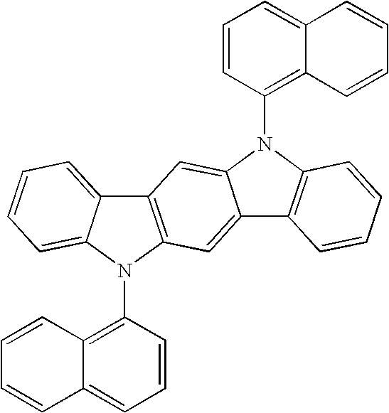 |
Synth. Met. 111, 421 (2000) |
| Isoindole compounds |
 |
Chem. Mater. 15, 3148 (2003) |
| Phosphorescent OLED host materials |
| Red hosts |
| Arylcarbazoles |
 |
Appl. Phys. Lett. 78, 1622 (2001) |
| Metal 8- hydroxyquinolates (e.g., Alq3, BAlq) |
 |
Nature 395, 151 (1998) |
 |
US20060202194 | |
 |
WO2005014551 | |
| Metal phenoxybenzothiazole compounds |
 |
Appl. Phys. Lett. 90, 123509 (2007) |
| Conjugated oligomers and polymers (e.g., polyfluorene) |
 |
Org. Electron. 1, 15 (2000) |
| Green hosts |
| Arylcarbazoles |
 |
Appl. Phys. Lett. 78, 1622 (2001) |
 |
US2003175553 | |
 |
WO2001039234 | |
| Aryltriphenylene compounds |
 |
US20060280965 |
 |
US20060280965 | |
| Polymers (e.g., PVK) |
 |
Appl. Phys. Lett. 77, 2280 (2000) |
| Spirofluorene compounds |
 |
WO2004093207 |
| Metal phenoxybenzooxazole compounds |
 |
WO05089025 |
 |
WO06132173 | |
 |
JP200511610 | |
| Spirofluorene- carbazole compounds |
 |
JP2007254297 |
 |
JP2007254297 | |
| Indolocabazoles |
 |
WO07063796 |
 |
WO07063754 | |
| 5-member ring electron deficient heterocycles (e.g., triazole, oxadiazole) |
 |
J. Appl. Phys. 90, 5048 (2001) |
 |
WO04107822 | |
| Metal phenoxypyridine compounds |
 |
WO05030900 |
| Blue hosts |
| Arylcarbazoles |
 |
Appl. Phys. Lett, 82, 2422 (2003) |
 |
US20070190359 | |
| Dibenzothiophene- carbazole compounds |
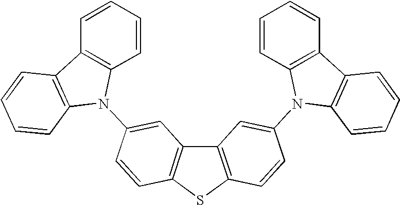 |
WO2006114966 |
| Phosphorescent dopants |
| Red dopants |
| Heavy metal porphyrins (e.g., PtOEP) |
 |
Nature 395, 151 (1998) |
| Iridium(III) organometallic complexes |
 |
Appl. Phys. Lett. 78, 1622 (2001) |
 |
US06835469 | |
 |
US06835469 | |
 |
US20060202194 | |
 |
US20060202194 | |
 |
US07087321 | |
 |
US07087321 | |
 |
Adv. Mater. 19, 739 (2007) | |
| Platinum(II) organometallic complexes |
 |
WO2003040257 |
| Osminum(III) complexes |
 |
Chem. Mater. 17, 3532 (2005) |
| Ruthenium(II) complexes |
 |
Adv. Mater. 17, 1059 (2005) |
| Green dopants |
| Iridium(III) organometallic complexes |  |
Inorg. Chem. 40, 1704 (2001) |
 |
US2002034656 | |
 |
US06687266 | |
 |
Chem. Mater. 16, 2480 (2004) | |
 |
US2007190359 | |
 |
US 2006008670 JP2007123392 | |
 |
Adv. Mater. 16, 2003 (2004) | |
 |
Angew. Chem. Int. Ed. 2006, 45, 7800 | |
| Pt(II) organometallic complexes |
 |
Appl. Phys. Lett. 86, 153505 (2005) |
 |
Appl. Phys. Lett. 86, 153505 (2005) | |
 |
Chem. Lett. 34, 592 (2005) | |
| Gold complexes |
 |
Chem. Commun. 2906 (2005) |
| Rhenium(III) complexes |
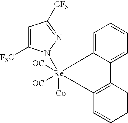 |
Inorg. Chem. 42, 1248 (2003) |
| Blue dopants |
| Iridium(III) organometallic complexes |
 |
WO2002002714 |
 |
WO2006009024 | |
 |
US2006251923 | |
 |
WO2006056418, US2005260441 | |
 |
US2007190359 | |
 |
US2002134984 | |
 |
Angew. Chem. Int. Ed. 47, 1 (2008) | |
 |
Chem. Mater. 18, 5119 (2006) | |
 |
Inorg. Chem. 46, 4308 (2007) | |
 |
WO05123873 | |
 |
WO05123873 | |
 |
WO07004380 | |
 |
WO06082742 | |
| Osmium(II) complexes |
 |
US2005260449 |
 |
Organometallics 23, 3745 (2004) | |
| Gold complexes |
 |
Appl. Phys. Lett. 74, 1361 (1999) |
| Platinum(II) complexes |
 |
WO06098120, WO06103874 |
| Exciton/hole blocking layer materials |
| Bathocuprine compounds (e.g., BCP, BPhen) |
 |
Appl. Phys. Lett. 75, 4 (1999) |
 |
Appl. Phys. Lett. 79, 449 (2001) | |
| Metal 8-hydroxyquinolates (e.g., BAlq) |
 |
Appl. Phys. Lett. 81, 162 (2002) |
| 5-member ring electron deficient heterocycles such as triazole, oxadiazole, imidazole, benzoimidazole |
 |
Appl. Phys. Lett. 81, 162 (2002) |
| Triphenylene compounds |
 |
US20050025993 |
| Fluorinated aromatic compounds |
 |
Appl. Phys. Lett. 79, 156 (2001) |
| Electron transporting materials |
| Anthracene- benzoimidazole compounds |
 |
WO03060956 |
| Anthracene- benzothiazole compounds |
 |
Appl. Phys. Lett. 89, 063504 (2006) |
| Metal 8- hydroxyquinolates (e.g., Alq3) |
 |
Appl. Phys. Lett. 51, 913 (1987) |
| Metal hydroxybenoquinolates |
 |
Chem. Lett. 5, 905 (1993) |
| Bathocuprine compounds such as BCP, BPhen, etc |
 |
Appl. Phys. Lett. 91, 263503 (2007) |
 |
Appl. Phys. Lett. 79, 449 (2001) | |
| 5-member ring electron deficient heterocycles (e.g., triazole, oxadiazole, imidazole, benzoimidazole) |
 |
Appl. Phys. Lett. 74, 865 (1999) |
 |
Appl. Phys. Lett. 55, 1489 (1989) | |
 |
Jpn. J. Apply. Phys. 32, L917 (1993) | |
| Silole compounds |
 |
Org. Electron. 4, 113 (2003) |
| Arylborane compounds |
 |
J. Am. Chem. Soc. 120, 9714 (1998) |
| Fluorinated aromatic |
 |
J. Am. Chem. Soc. 122, 1832 (2000) |
Claims (11)


Priority Applications (1)
| Application Number | Priority Date | Filing Date | Title |
|---|---|---|---|
| US12/174,286 US8372526B2 (en) | 2008-07-16 | 2008-07-16 | Intermediate connector for stacked organic light emitting devices |
Applications Claiming Priority (1)
| Application Number | Priority Date | Filing Date | Title |
|---|---|---|---|
| US12/174,286 US8372526B2 (en) | 2008-07-16 | 2008-07-16 | Intermediate connector for stacked organic light emitting devices |
Publications (2)
| Publication Number | Publication Date |
|---|---|
| US20100013378A1 US20100013378A1 (en) | 2010-01-21 |
| US8372526B2 true US8372526B2 (en) | 2013-02-12 |
Family
ID=41529710
Family Applications (1)
| Application Number | Title | Priority Date | Filing Date |
|---|---|---|---|
| US12/174,286 Active 2031-01-20 US8372526B2 (en) | 2008-07-16 | 2008-07-16 | Intermediate connector for stacked organic light emitting devices |
Country Status (1)
| Country | Link |
|---|---|
| US (1) | US8372526B2 (en) |
Cited By (1)
| Publication number | Priority date | Publication date | Assignee | Title |
|---|---|---|---|---|
| US20170125718A1 (en) * | 2012-09-26 | 2017-05-04 | Universal Display Corporation | Three stack hybrid white oled for enhanced efficiency and lifetime |
Families Citing this family (8)
| Publication number | Priority date | Publication date | Assignee | Title |
|---|---|---|---|---|
| US20100225252A1 (en) * | 2008-10-01 | 2010-09-09 | Universal Display Corporation | Novel amoled display architecture |
| US8827488B2 (en) | 2008-10-01 | 2014-09-09 | Universal Display Corporation | OLED display architecture |
| US9385167B2 (en) * | 2008-10-01 | 2016-07-05 | Universal Display Corporation | OLED display architecture |
| US8334545B2 (en) | 2010-03-24 | 2012-12-18 | Universal Display Corporation | OLED display architecture |
| US8957579B2 (en) | 2012-09-14 | 2015-02-17 | Universal Display Corporation | Low image sticking OLED display |
| US8766531B1 (en) * | 2012-12-14 | 2014-07-01 | Universal Display Corporation | Wearable display |
| KR101525459B1 (en) * | 2013-11-14 | 2015-06-03 | 코닝정밀소재 주식회사 | Tandem white organic light emitting device |
| CN120614940A (en) * | 2024-03-08 | 2025-09-09 | 宁德时代新能源科技股份有限公司 | Tandem solar cells, photovoltaic modules, photovoltaic systems, electrical devices and power generation devices |
Citations (16)
| Publication number | Priority date | Publication date | Assignee | Title |
|---|---|---|---|---|
| US5707745A (en) | 1994-12-13 | 1998-01-13 | The Trustees Of Princeton University | Multicolor organic light emitting devices |
| US5917280A (en) | 1997-02-03 | 1999-06-29 | The Trustees Of Princeton University | Stacked organic light emitting devices |
| US6107734A (en) * | 1998-05-20 | 2000-08-22 | Idemitsu Kosan Co., Ltd. | Organic EL light emitting element with light emitting layers and intermediate conductive layer |
| US6232714B1 (en) | 1997-05-20 | 2001-05-15 | The Trustees Of Princeton University | Saturated full color stacked organic light emitting devices |
| US6337492B1 (en) | 1997-07-11 | 2002-01-08 | Emagin Corporation | Serially-connected organic light emitting diode stack having conductors sandwiching each light emitting layer |
| US20040113547A1 (en) | 1999-12-31 | 2004-06-17 | Se-Hwan Son | Electroluminescent devices with low work function anode |
| US20050029933A1 (en) * | 2002-02-15 | 2005-02-10 | Eastman Kodak Compamy | Cascaded organic electroluminescent devices with color filters |
| US6936961B2 (en) | 2003-05-13 | 2005-08-30 | Eastman Kodak Company | Cascaded organic electroluminescent device having connecting units with N-type and P-type organic layers |
| WO2005109542A1 (en) | 2004-05-11 | 2005-11-17 | Lg Chem. Ltd. | Organic electronic device |
| US6991859B2 (en) | 2003-03-18 | 2006-01-31 | Eastman Kodak Company | Cascaded organic electroluminescent devices |
| JP2006066379A (en) * | 2004-07-30 | 2006-03-09 | Sanyo Electric Co Ltd | Organic electroluminescence element and organic electroluminescence display device |
| US7075231B1 (en) | 2005-01-03 | 2006-07-11 | Eastman Kodak Company | Tandem OLEDs having low drive voltage |
| US20060250079A1 (en) * | 2005-04-05 | 2006-11-09 | The Hong Kong University Of Science And Technology | Intermediate layers treated by cf4-plasma for stacked organic light-emitting devices |
| US7173369B2 (en) | 1994-12-13 | 2007-02-06 | The Trustees Of Princeton University | Transparent contacts for organic devices |
| US20070046189A1 (en) * | 2005-08-31 | 2007-03-01 | Eastman Kodak Company | Intermediate connector for a tandem OLED device |
| US20070103066A1 (en) | 2005-11-04 | 2007-05-10 | D Andrade Brian W | Stacked OLEDs with a reflective conductive layer |
-
2008
- 2008-07-16 US US12/174,286 patent/US8372526B2/en active Active
Patent Citations (17)
| Publication number | Priority date | Publication date | Assignee | Title |
|---|---|---|---|---|
| US5721160A (en) | 1994-12-13 | 1998-02-24 | The Trustees Of Princeton University | Multicolor organic light emitting devices |
| US5707745A (en) | 1994-12-13 | 1998-01-13 | The Trustees Of Princeton University | Multicolor organic light emitting devices |
| US7173369B2 (en) | 1994-12-13 | 2007-02-06 | The Trustees Of Princeton University | Transparent contacts for organic devices |
| US5917280A (en) | 1997-02-03 | 1999-06-29 | The Trustees Of Princeton University | Stacked organic light emitting devices |
| US6232714B1 (en) | 1997-05-20 | 2001-05-15 | The Trustees Of Princeton University | Saturated full color stacked organic light emitting devices |
| US6337492B1 (en) | 1997-07-11 | 2002-01-08 | Emagin Corporation | Serially-connected organic light emitting diode stack having conductors sandwiching each light emitting layer |
| US6107734A (en) * | 1998-05-20 | 2000-08-22 | Idemitsu Kosan Co., Ltd. | Organic EL light emitting element with light emitting layers and intermediate conductive layer |
| US20040113547A1 (en) | 1999-12-31 | 2004-06-17 | Se-Hwan Son | Electroluminescent devices with low work function anode |
| US20050029933A1 (en) * | 2002-02-15 | 2005-02-10 | Eastman Kodak Compamy | Cascaded organic electroluminescent devices with color filters |
| US6991859B2 (en) | 2003-03-18 | 2006-01-31 | Eastman Kodak Company | Cascaded organic electroluminescent devices |
| US6936961B2 (en) | 2003-05-13 | 2005-08-30 | Eastman Kodak Company | Cascaded organic electroluminescent device having connecting units with N-type and P-type organic layers |
| WO2005109542A1 (en) | 2004-05-11 | 2005-11-17 | Lg Chem. Ltd. | Organic electronic device |
| JP2006066379A (en) * | 2004-07-30 | 2006-03-09 | Sanyo Electric Co Ltd | Organic electroluminescence element and organic electroluminescence display device |
| US7075231B1 (en) | 2005-01-03 | 2006-07-11 | Eastman Kodak Company | Tandem OLEDs having low drive voltage |
| US20060250079A1 (en) * | 2005-04-05 | 2006-11-09 | The Hong Kong University Of Science And Technology | Intermediate layers treated by cf4-plasma for stacked organic light-emitting devices |
| US20070046189A1 (en) * | 2005-08-31 | 2007-03-01 | Eastman Kodak Company | Intermediate connector for a tandem OLED device |
| US20070103066A1 (en) | 2005-11-04 | 2007-05-10 | D Andrade Brian W | Stacked OLEDs with a reflective conductive layer |
Non-Patent Citations (21)
| Title |
|---|
| A. Werner, M. Burghart, S. Murano, O. Schneider, T. Stubinger, M. Limmert, and J. Blochwitz-Nimoth, "White OLED structures using molecularly doped charge transport layers," San Francisco, CA, United States, 2006 (Society for Information Display, San Jose, CA 95112-4006, United States), p. 1078-1081. |
| B. D'Andrade and J. J. Brown, "White phosphorescent organic light emitting devices for display applications," Kissimmee, FL, United States, 2006 (International Society for Optical Engineering, Bellingham, WA, WA 98227-0010, United States), p. 622514. |
| C.-C. Chang, J.-F. Chen, S.-W. Hwang, and C. H. Chen, "Highly efficient white organic electroluminescent devices based on tandem architecture," Applied Physics Letters 87, 253501 (2005). |
| C.-W. Chen, E. H.-E. Wu, C.-W. Chu, C.-C. Wu, and Y. Yang, "The mechanism and effective connecting architecture for tandem organic light-emitting devices," San Diego, CA, United States, 2005 (International Society for Optical Engineering, Bellingham, WA, WA 98227-0010, United States), p. 1-8. |
| G. Schwartz, K. Walzer, M. Pfeiffer, and K. Leo, "High efficiency white organic light emitting diodes combining fluorescent and phosphorescent emitter systems," Strasbourg, France, 2006 (International Society for Optical Engineering, Bellingham WA, WA 98227-0010, United States), p. 61920. |
| H. Kanno, Y. Hamada, K. Nishimura, K. Okumoto, N. Saito, H. Ishida, H. Takahashi, K. Shibata, and K. Mameno, "High efficiency stacked organic light-emitting diodes employing Li 2O as a connecting layer," Japanese Journal of Applied Physics, Part 1: Regular Papers and Short Notes and Review Papers 45, 9219-9223 (2006). |
| H. Y. Chu, J.-I. Lee, L.-M. Do, T. Zyung, B.-J. Jung, H.-K. Shim, and J. Jang, "Organic white light emitting devices with an RGB stacked multilayer structure," Sendai, Japan, 2003 (Taylor and Francis Inc., Philadelphia PA, PA 19106, United States), p. 119-125. |
| Ho et al., "Highly efficient p-i-n white organic light emitting devices with tandem structure," Appl. Phys. Lett., 91, 233507 (2007). |
| J. X. Sun, X. L. Zhu, H. J. Peng, M. Wong, and H. S. Kwok, "Bright and efficient white stacked organic light-emitting diodes," Organic Electronics: physics, materials, applications 8, 305-310 (2007). |
| L.-S. Liao, K. P. Klubek, M. J. Helber, L. Cosimbescu, and D. L. Comfort, Distinguished paper: "High-efficiency tandem blue OLEDs," San Francisco, CA, United States, 2006 (Society for Information Display, San Jose, CA 95112-4006, United States), p. 1176-1179. |
| L.-S. Liao, W. K. Slusarek, T. K. Hatwar, M. L. Ricks, and D. L. Comfort, "Tandem organic light-emitting diode using hexaazatriphenylene hexacarbonitrile in the intermediate connector," Advanced Materials 20, 324-329 (2008). |
| Liao et al., "Tandem white OLEDs combining fluorescent and phosphorescent emission," SID 08 Digest, pp. 818-821, (2008). |
| Machine translation of JP2006-066379. Date of publication: Mar. 9, 2006. * |
| S. Murano, M. Burghart, J. Birnstock, P. Wellmann, M. Vehse, A. Werner, T. Canzler, T. Stubinger, G. He, M. Pfeiffer, and H. Boerner, "Highly efficient white OLEDs for lighting applications," San Diego, CA, United States, 2005 (International Society for Optical Engineering, Bellingham, WA, WA 98227-0010, United States), p. 1-8. |
| Sun et al., "Effective intermediate layers for highly efficient stacked organic light-emitting devices," Appl. Phys. Lett. 87, 093504 (2005). |
| T. K. Hatwar, J. P. Spindler, and S. A. Van Slyke, "Low-voltage white tandem structures for fabricating RGBW AMOLED displays," San Francisco, CA, United States, 2006 (Society for Information Display, San Jose, CA 95112-4006, United States), p. 1939-1942. |
| T. K. Hatwar, J. P. Spindler, and S. A. Van Slyke, 1447: "High performance tandem OLEDs for large area full color AM displays and lighting applications," Daegu, South Korea, 2006 (Korean Information Display Society, 635-4 Yeogasm-Dong, Kangnam-gu, Seoul, 135-703, South Korea), p. 1577-1582. |
| T. W. Canzler, M. Burghart, S. Murano, J. Blochwitz-Nimoth, B. D'Andrade, M. Hack, and J. J. Brown, "Highly power efficient organic light-emitting devices enabled by phosphorescent and p-i-n. technologies," San Diego, CA, United States, 2006 (International Society for Optical Engineering, Bellingham WA, WA 98227-0010, United States), p. 633311. |
| T.-W. Lee, T. Noh, B.-K. Choi, M.-S. Kim, D. W. Shin, and J. Kido, "High-efficiency stacked white organic light-emitting diodes," Applied Physics Letters 92, 043301 (2008). |
| Walzer et al., "Highly efficient organic devices based on electrically doped transport layers," Chem. Rev. 2007, 107, 1233-1271. |
| Zheng at al., "An effective intermediate Al/Au electrode for stacked color-tunable organic light emitting devices," Appl. Phys. A 91, 501-506 (2008). |
Cited By (3)
| Publication number | Priority date | Publication date | Assignee | Title |
|---|---|---|---|---|
| US20170125718A1 (en) * | 2012-09-26 | 2017-05-04 | Universal Display Corporation | Three stack hybrid white oled for enhanced efficiency and lifetime |
| US11177452B2 (en) * | 2012-09-26 | 2021-11-16 | Universal Display Corporation | Three stack hybrid white OLED for enhanced efficiency and lifetime |
| US12035551B2 (en) | 2012-09-26 | 2024-07-09 | Universal Display Corporation | Three stack hybrid white OLED for enhanced efficiency and lifetime |
Also Published As
| Publication number | Publication date |
|---|---|
| US20100013378A1 (en) | 2010-01-21 |
Similar Documents
| Publication | Publication Date | Title |
|---|---|---|
| US11716902B2 (en) | Organic electroluminescent materials and devices | |
| US12295199B2 (en) | Phosphorescence-sensitized delayed fluorescence light emitting system | |
| US20240147834A1 (en) | Organic electroluminescent materials and devices | |
| US9627631B2 (en) | Organic electroluminescent materials and devices | |
| US8513658B2 (en) | White phosphorescent organic light emitting devices | |
| US11289659B2 (en) | Organic electroluminescent materials and devices | |
| US8367223B2 (en) | Heteroleptic phosphorescent emitters | |
| US9140428B2 (en) | Triplet-triplet annihilation up-conversation for display and lighting applications | |
| US8440326B2 (en) | Hole transport materials containing triphenylene | |
| US9175211B2 (en) | Phosphorescent materials | |
| US8053770B2 (en) | Emissive layer patterning for OLED | |
| US8040053B2 (en) | Organic light emitting device architecture for reducing the number of organic materials | |
| US10256427B2 (en) | Efficient organic electroluminescent devices | |
| US8778511B2 (en) | OLED stability via doped hole transport layer | |
| US8372526B2 (en) | Intermediate connector for stacked organic light emitting devices | |
| US20060279204A1 (en) | OLEDs utilizing direct injection to the triplet state | |
| US9054343B2 (en) | Fine tuning of emission spectra by combination of multiple emitter spectra | |
| US20150076470A1 (en) | Luminescent Cyclometallated Iridium (III) Complexes Having Acetylide Ligands |
Legal Events
| Date | Code | Title | Description |
|---|---|---|---|
| AS | Assignment |
Owner name: UNIVERSAL DISPLAY CORPORATION, NEW JERSEY Free format text: ASSIGNMENT OF ASSIGNORS INTEREST;ASSIGNOR:D'ANDRADE, BRIAN;REEL/FRAME:028836/0748 Effective date: 20081001 |
|
| FEPP | Fee payment procedure |
Free format text: PAYOR NUMBER ASSIGNED (ORIGINAL EVENT CODE: ASPN); ENTITY STATUS OF PATENT OWNER: LARGE ENTITY |
|
| STCF | Information on status: patent grant |
Free format text: PATENTED CASE |
|
| FPAY | Fee payment |
Year of fee payment: 4 |
|
| MAFP | Maintenance fee payment |
Free format text: PAYMENT OF MAINTENANCE FEE, 8TH YEAR, LARGE ENTITY (ORIGINAL EVENT CODE: M1552); ENTITY STATUS OF PATENT OWNER: LARGE ENTITY Year of fee payment: 8 |
|
| MAFP | Maintenance fee payment |
Free format text: PAYMENT OF MAINTENANCE FEE, 12TH YEAR, LARGE ENTITY (ORIGINAL EVENT CODE: M1553); ENTITY STATUS OF PATENT OWNER: LARGE ENTITY Year of fee payment: 12 |