US8344295B2 - Nanosoldering heating element - Google Patents
Nanosoldering heating element Download PDFInfo
- Publication number
- US8344295B2 US8344295B2 US12/579,128 US57912809A US8344295B2 US 8344295 B2 US8344295 B2 US 8344295B2 US 57912809 A US57912809 A US 57912809A US 8344295 B2 US8344295 B2 US 8344295B2
- Authority
- US
- United States
- Prior art keywords
- heating element
- substrate
- layer
- wall
- etching
- Prior art date
- Legal status (The legal status is an assumption and is not a legal conclusion. Google has not performed a legal analysis and makes no representation as to the accuracy of the status listed.)
- Expired - Fee Related, expires
Links
Images


Classifications
-
- H—ELECTRICITY
- H05—ELECTRIC TECHNIQUES NOT OTHERWISE PROVIDED FOR
- H05B—ELECTRIC HEATING; ELECTRIC LIGHT SOURCES NOT OTHERWISE PROVIDED FOR; CIRCUIT ARRANGEMENTS FOR ELECTRIC LIGHT SOURCES, IN GENERAL
- H05B3/00—Ohmic-resistance heating
- H05B3/10—Heater elements characterised by the composition or nature of the materials or by the arrangement of the conductor
- H05B3/12—Heater elements characterised by the composition or nature of the materials or by the arrangement of the conductor characterised by the composition or nature of the conductive material
- H05B3/14—Heater elements characterised by the composition or nature of the materials or by the arrangement of the conductor characterised by the composition or nature of the conductive material the material being non-metallic
- H05B3/145—Carbon only, e.g. carbon black, graphite
-
- H—ELECTRICITY
- H05—ELECTRIC TECHNIQUES NOT OTHERWISE PROVIDED FOR
- H05B—ELECTRIC HEATING; ELECTRIC LIGHT SOURCES NOT OTHERWISE PROVIDED FOR; CIRCUIT ARRANGEMENTS FOR ELECTRIC LIGHT SOURCES, IN GENERAL
- H05B3/00—Ohmic-resistance heating
- H05B3/10—Heater elements characterised by the composition or nature of the materials or by the arrangement of the conductor
- H05B3/12—Heater elements characterised by the composition or nature of the materials or by the arrangement of the conductor characterised by the composition or nature of the conductive material
- H05B3/14—Heater elements characterised by the composition or nature of the materials or by the arrangement of the conductor characterised by the composition or nature of the conductive material the material being non-metallic
-
- H—ELECTRICITY
- H05—ELECTRIC TECHNIQUES NOT OTHERWISE PROVIDED FOR
- H05B—ELECTRIC HEATING; ELECTRIC LIGHT SOURCES NOT OTHERWISE PROVIDED FOR; CIRCUIT ARRANGEMENTS FOR ELECTRIC LIGHT SOURCES, IN GENERAL
- H05B2214/00—Aspects relating to resistive heating, induction heating and heating using microwaves, covered by groups H05B3/00, H05B6/00
- H05B2214/04—Heating means manufactured by using nanotechnology
Definitions
- Providing heat to a very small area is performed in many fields, such as heat activated polymerization on a surface, local chemical transformation, and nano-soldering.
- heat activated polymerization on a surface
- local chemical transformation and nano-soldering.
- nano-technology may be applied to applications for providing heat to a very small area.
- a carbon nanotube or a new carbon material, such as graphene, is a prospective for such applications due to its high electrical conductivity and small size.
- a heating element includes a substrate having at least one wall extending from a portion thereof so as to define a series of a contiguously connected top surfaces thereby, and a conducting layer including conducting materials and being substantially arranged upon the top surfaces, wherein the outermost portion of the at least one wall has an etched portion thereon.
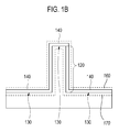
- FIG. 1A shows a perspective view of an illustrative embodiment of a heating element.
- FIG. 1B shows a front view of an illustrative embodiment of a heating element.
- FIG. 2 shows (a) an outermost portion of a wall of the heating element shown in FIG. 1 and (b) an enlarged view of the outermost portion of the wall showing etched portions within a gridlike structure of carbon nanotubes (CNTs).
- CNTs carbon nanotubes
- FIG. 3 shows a perspective view of an illustrative embodiment of a heating element to which a graphene sheet is applied.
- FIG. 4 shows a perspective view of an illustrative embodiment of a heating element having three walls.
- FIG. 5 shows an exploded perspective view of an illustrative embodiment of the heating element shown in FIG. 1 applied to polymerization.
- FIG. 6 shows an exploded perspective view of an illustrative embodiment where the heating element shown in FIG. 1 is applied to nanosoldering.
- FIG. 7 shows a flow diagram of an illustrative embodiment of a method for manufacturing a heating element that provides heat to a small area.
- FIG. 8 shows a flow diagram of an illustrative embodiment of a method for forming at least one wall.
- FIGS. 9A-9H show a series of diagrams illustrating the method shown in FIG. 8 .
- FIG. 10 shows a flow diagram of another illustrative embodiment of a method for forming at least one wall on the substrate.
- FIGS. 11A-11C show a series of diagrams illustrating the method shown in FIG. 10 .
- Heating elements with nano-scale heating areas may be applied to fields such as heat activated polymerization on a surface, local chemical transformation, and nano-soldering.
- Techniques described in the present disclosure employ a novel heating element to locally apply heat to a nano-sized small area.
- a heating element has a CNT film arranged on top surfaces thereof, at least one prominent portion of the CNT film being etched so that it has lower conductivity than other remaining portions.
- the etched portion may operate as resistance and thus be selectively heated. Since the etched portion has a width on the order of nanometers, the area heated is significantly small.
- FIGS. 1A and 1B respectively show a perspective view and front view of an illustrative embodiment of a heating element 100 that may be used to provide heat to a very small area.
- heating element 100 may include a substrate 110 that has a prominent portion 120 (hereinafter referred to as “wall”).
- wall 120 may extend from a portion of substrate 110 in the direction substantially perpendicular with respect to other portions of substrate 110 and define contiguously connected top surfaces 130 .
- other portions may include parts of substrate 110 that do not form wall 120 .
- substrate 110 may be fabricated using one of a silicon wafer, glass, or quartz.
- Heating element 100 may further include a conducting layer.
- a CNT film 140 may serve as a conducting layer and may be arranged on top surfaces 130 to coat substrate 110 with carbon nanotubes (CNTs).
- CNTs include high-aspect ratio microscopic carbon materials, each of which has an outer diameter on the order of nanometers and a length of about 0.5 nanometers to tens of micrometers.
- each of the CNTs may have a shape of a hollow cylinder having regularly arranged carbon atoms.
- CNTs with the above-described features may readily provide an electric field concentration and may provide a high emission current density, and may have highly stable chemical and physical characteristics.
- An outermost portion 150 of wall 120 may include one or more etched portions 144 that have lower conductivity than other remaining portions of wall 120 . If a certain voltage is applied to heating element 100 through an external circuit (not shown), a predetermined current may flow through heating element 100 , so that etched portions 144 operate as resistance and result in selective heating thereof.
- FIG. 2 shows an enlarged view of an illustrative embodiment of one part 151 of outermost portion 150 of wall 120 of heating element 100 .
- CNT film 140 may have a grid-like structure of CNTs, and at least one portion of the grid-like structure of CNTs disposed on outermost portion 150 may be broken to form one or more etched portions 144 .
- the broken structures of one or more etched portions 144 change the electrical properties of etched portions 144 to increase resistivity of etched portions 144 .
- conductivity of etched portions 144 may become lower than other portions of wall 120 . In this case, if a certain voltage is applied to heating element 100 , etched portions 144 may operate as resistance and result in selective heating thereof.
- heating element 100 may have a width on the order of nanometers, the area heated in heating element 100 (i.e., substantially etched portions 144 ) may be significantly small. Heating element 100 having the above-described structure may be suitable for providing heat to a small area for such applications as nano-soldering and local chemical transformation.
- CNT film 140 may include various single-walled carbon nanotubes whose electrical properties are metallic or semiconducting, i.e., semiconducting single-walled carbon nanotubes (SWNTs) or metallic SWNTs.
- substrate 110 may be functionalized by a suitable silane so that substrate 110 can have the desired properties. The functionalization introduces chemical functional groups included in the silane to substrate 110 for the desired property. Particularly, if substrate 110 is functionalized by aromatic molecules such as phenyl-terminated silane which is known to interact and selectively bind to metallic SWNTs, metallic SWNTs may be selectively absorbed into substrate 110 . In this case, heating element 100 may have higher conductivity compared to one without phenyl-terminated silane. Below is the formula of phenyl-terminated silane used here. Other aromatic molecules for functionalizing substrate 100 may include porphyrins, phthalocyanines, or perylenes.
- heating element 100 may have a protection layer 160 substantially arranged upon CNT film 140 .
- the protection layer 160 may be employed to increase the adhesion of CNT film 140 on substrate 110 . Due to the existence of the protection layer 160 , when the electricity flows to heating element 100 from an outside circuit (not shown), the surface barrier of electrons may be substantially increased upon emission of the electrons. Accordingly, the emission efficiency can be significantly reduced. This may enhance the adhesive strength between substrate 110 having wall 120 and CNT film 140 .
- a protection layer 160 may be applied to the faces of CNT film 140 at a uniform pressure across the entire surface so that the protection layer 160 may be substantially deposited and maintained thereupon. The thickness of the protection layer 160 may be less than 100 nm.
- the protection layer 160 may include insulation materials such as silicon dioxide (SiO2), a fluorosilicate glass (FSG), a tetraethyl orthosilicate (TEOS) oxide, a silanol (SiOH), a flowable oxide (FOx), a bottom anti-reflective coating (BARC), an anti-reflective coating (ARC), a photoresist (PR), a near-frictionless carbon (NFC), a silicon carbide (SiC), a silicon oxycarbide (SiOC), and/or a carbon-doped silicon oxide (SiCOH).
- heating element 100 may have an insulation layer 170 arranged substantially between the top surfaces 130 and the conducting layer 140 .
- FIG. 3 shows a perspective view of an illustrative embodiment of a heating element 300 having a graphene sheet 340 on a substrate 310 .
- heating element 300 may include substrate 310 which has a prominent portion 320 (hereinafter referred to as “wall”).
- Wall 320 has a similar structure to wall 120 illustrated in FIG. 1 and thus detailed descriptions thereof are omitted.
- substrate 310 may be fabricated using one of a silicon wafer, glass, or quartz.
- Graphene sheet 340 may be arranged on top surfaces 330 of substrate 310 to coat substrate 310 with graphene.
- Graphene sheet 340 includes polycyclic aromatic molecules in which multiple carbon atoms are covalently bound to each other.
- the covalently bound carbon atoms form 6-membered rings as a repeating unit and may additionally form 5-membered rings and/or 7-membered rings. Accordingly, graphene sheet 340 may appear as if the covalently bound carbon atoms form a single layer thereby.
- Graphene sheet 340 may have various structures depending on the amount of 5-membered rings and/or 7-membered rings included therein.
- Graphene sheet 340 may have one or more layers of graphene, which may have a thickness of about 100 nm.
- Graphene sheet 340 with the above-described features may readily provide an electric field concentration, may provide a high emission current density, and have highly stable chemical and physical characteristics.
- An outermost portion 322 of wall 320 may have one or more etched portions 324 .
- oxygen plasma treatment may be conducted to etch graphene sheet 340 . Since graphene sheet 340 is a sheet of bonded carbons, some of the frame structures of carbons in etched portion 324 are broken. Thus, the conductivity of etched portion 324 may be lower than that of other portions.
- FIG. 4 shows a perspective view of an illustrative embodiment of a heating element 400 having more than one wall (for example, three walls 420 , 422 , and 424 ) on substrate 410 .
- Heating element 400 has a similar or substantially identical to heating element 100 except that three walls 420 , 422 , and 424 are formed on substrate 410 . Thus, detailed descriptions thereof are omitted.
- three walls 420 , 422 , and 424 have width and height of several hundreds of nanometers.
- Heating element 400 has contiguously connected top surfaces 430 , and on top surfaces 430 , CNT film 440 may be arranged.
- each of walls 420 , 422 , and 424 has one or more etched portions 433 having the increased resistivity. If voltage is applied to heating element 400 through an outside circuit (not shown), etched portions 433 may be selectively heated. It will be appreciated by those skilled in the art that any variety of walls formed in heating element 400 may be employed.
- FIG. 5 illustrates an embodiment where a heating element 500 is used for a polymerization.
- heating element 500 may have a structure similar to either one of heating elements 100 and 300 illustrated in FIGS. 1 and 3 , respectively.
- an outermost portion 508 of a wall 504 may be etched using the same methods as described above with respect to FIGS. 1 to 3 , so that the conductivity of outermost portion 508 may be lower than that of the other portions of wall 504 .
- a polymer material such as a polymer film 510 may be positioned so that one planar surface thereof is faced with outermost portion 508 of wall 504 as shown in FIG. 5 .
- polymer film 510 may be positioned in contact with outermost portion 508 of wall 504 or positioned at such a certain distance to outermost portion 508 of wall 504 that heat generated from outermost portion 508 may be effectively transferred to polymer film 510 .
- the electricity flows to heating element 500 from an outside circuit 520 the etched portions in outermost portion 508 of wall 504 may be selectively heated and the heat generated from outermost portion 508 may be transferred to polymer film 510 .
- heat-activated initiators in polymer film 510 may be activated, thereby conducting polymerization.
- FIG. 6 illustrates another embodiment where a heating element 600 is used for nano-soldering.
- heating element 600 may have a structure similar to either one of heating elements 100 and 300 illustrated in FIGS. 1 and 3 , respectively.
- an outermost portion of a wall 604 may be etched using the same methods as described above with respect to FIGS. 1 to 3 , so that the conductivity of outermost portion may be lower than that of other portions of wall 604 .
- an object e.g., nano-scale circuit with nano-materials to be soldered may be positioned so that the nano-materials to be soldered are faced with outermost portion of wall 604 as shown in FIG. 6 .
- heating element 600 may be arranged so that outermost portion of wall 604 is positioned substantially in contact with or at such a distance to an area 610 of an object to be soldered, where metal particles 614 are pre-arranged between nano-materials 602 to be coupled to each other by soldering.
- electricity from an outside circuit 620 flows to heating element 600 , the etched portions in outermost portion of wall 604 are heated to solder nano-materials 602 with metal particles 614 .
- metal particles 614 may be formed on a nanoscale. In such a case, since the melting point of metal particles 614 is much lower than a bulk metal material, metal particles 614 are likely to be melted even with a small amount of heat generated from outermost portion of wall 604 .
- FIG. 7 illustrates a flow diagram of an illustrative embodiment of a method for manufacturing a heating element that provides heats to a small area.
- the heating element may be manufactured by forming at least one wall on a substrate (block 710 ), coating a top surface of the wall with coating materials (block 720 ), and etching at least a portion of the at least one wall (block 730 ).
- FIG. 8 and FIGS. 9A-9H a detail description for the method of FIG. 7 will be provided hereinafter.
- FIG. 8 shows a flow diagram of an illustrative embodiment of a method for forming at least one wall on a substrate.
- FIGS. 9A-9H show a series of diagrams illustrating the method shown in FIG. 8 .
- an etch mask layer 912 is arranged upon a substrate 910 , such as a silicon wafer, glass, or quartz, by using any of a variety of well-known fabrication process such as chemical vapor deposition or photolithographic techniques.
- Etch mask layer 912 may be thick enough to provide a pinhole-free etch barrier for subsequent processing and may be sufficiently thin to accurately register the extreme submicron dimensions.
- Etch mask layer 912 may include materials, such as Si 3 N 4 , SiO 2 , or tungsten.
- a photoresist layer 914 is arranged upon etch mask layer 912 (block 820 ).
- photoresist layer 914 may be about 150 nm to about 200 nm thick. Referring to FIG. 9C , photoresist layer 914 is exposed using conventional lithography techniques to form an appropriate lithography pattern 916 . Photoresist layer 914 is etched (block 840 ) as shown in FIG. 9D so that lithography pattern 916 remains on etch mask layer 912 . In FIG. 9E , etch mask layer 912 is etched (block 850 ) in a manner so that a portion of etch mask layer 912 arranged below lithography pattern 916 remains on substrate 910 .
- etch mask layer 912 includes nitride material
- CF 4 etchant may be used to etch mask layer 912 .
- the remaining photoresist layer i.e., lithography pattern 916
- suitable etching process block 860
- FIG. 9G illustrates substrate 910 prior to etching and, as shown in FIG. 9G an etching process is performed on substrate 910 (block 870 ) so that a portion of substrate 910 arranged below etch mask layer 912 remains while the other portions of substrate 910 are etched.
- a wall 911 (i.e., prominent portion) is formed between etch mask layer 912 and the un-etched portion of substrate 910 , as shown in FIG. 9G .
- the etching process in blocks 840 , 850 , and 870 may be conducted using well-known etching techniques such as a KOH etching process, or plasma etching.
- the regions of exposed substrate 910 , on which no wall 911 is formed, are etched with a highly anisotropic etching process such as KOH wet etching.
- KOH wet etching such as KOH wet etching.
- other anisotropic etching processes such as reactive-ion etching or ion-milling may be used.
- Etch mask layer 912 is removed by a suitable etching process (block 880 ) as shown in FIG. 9H , so that wall 911 remains on substrate 910 . Since wall 911 has a material identical to that of substrate 910 and is formed by etching some portions of substrate 910 , a series of continuously connected top surfaces 130 is formed on substrate 910 .
- a conducting layer is arranged on top surfaces which are defined by the substrate and the wall (block 720 ).
- a conduction layer such as a CNT film may be arranged on the top surfaces.
- the CNT film may be formed by any one of the transfer, coating, spraying, or screen printing methods.
- the top surfaces may be coated with CNTs by using conventional coating techniques such as wet coating including spraying, dipping and roll coating, or dry coating.
- a graphene sheet may be used as the conducting layer.
- the graphene sheet may be prepared by a micromechanical method or a SiC thermal decomposition.
- a graphene sheet separated from graphite can be prepared on the surface of a tape (e.g. tape sold under the trade name “Scotch”) by attaching the tape to a graphite sample and detaching the tape.
- a tape e.g. tape sold under the trade name “Scotch”
- SiC thermal decomposition SiC single crystal is heated to remove Si by decomposition of the SiC on the surface, and then residual carbon C forms a graphene sheet.
- An outermost portion of the wall is etched (block 730 ).
- plasma etching such as O 2 plasma etching, or methane plasma etching may be conducted to etch the outermost portion of the wall.
- the carbon structures of conducting materials i.e., CNTs or graphenes, are broken, and thus the conductivity of the outermost portion of the wall becomes lower than that of the other portions.
- a protection layer may be further arranged on the conducting layer.
- the protection layer may be formed by sputtering or by a vapor deposition method such as Chemical Vapor Deposition (CVD).
- FIG. 10 shows a flow diagram of another illustrative embodiment of a method for forming multiple walls on the substrate.
- FIGS. 11A-11C show a series of diagrams illustrating the method shown in FIG. 10 .
- multiple nanostructures 1110 each made of silicon or chromium are located on a substrate 1120 .
- Nanostructures 1110 may be prepared in advance using any of a variety of well-known fabrication techniques, such as lithography, etching, or deposition techniques.
- a plate 1140 is placed above nanostructures 1110 (block 1020 ) so that a certain gap is formed between nanostructures 1110 and plate 1140 .
- local spacers 1130 may be arranged on substrate 1120 for plate 1140 to maintain a predetermined gap with nanostructures 1110 .
- plate 1140 is illustrated as being detached from the remaining structures (local spacers 1130 , nanostructure 1110 , substrate 1120 , etc.) Nanostructures 1110 are melted and liquefied by heating (block 1030 ).
- heating may be performed on plate 1140 by using a laser beam 1150 of a certain wavelength (in the form of either a flood or masked beam), which emits through plate 1140 a certain amount of energy (as depicted in FIG. 11A ) to melt nanostructures 1110 (in the solid phase) at a low temperature.
- Both pulsed and continuous-wave lasers may be used to melt nanostructures 1110 .
- the interaction between nanostructures 1110 and plate 1140 may make the molten nanostructures 1110 rise up (against the liquid surface tension) to reach plate 1140 , which forms new shapes of nanostructures 1160 , resulting in a greater height and a narrower line width, smooth edges, vertical sidewalls and a flat top.
- cooling and removal processes are performed, thereby removing spacers 1130 and plate 140 and completing formation of walls 1170 on substrate 1120 as shown in FIG. 11C . Spacers 1130 and plate 140 may not be necessary after walls 1170 are formed on substrate 1120 .
- a group having 1-3 cells refers to groups having 1, 2, or 3 cells.
- a group having 1-5 cells refers to groups having 1, 2, 3, 4, or 5 cells, and so forth.
Abstract
Description

Claims (20)
Priority Applications (4)
| Application Number | Priority Date | Filing Date | Title |
|---|---|---|---|
| US12/579,128 US8344295B2 (en) | 2009-10-14 | 2009-10-14 | Nanosoldering heating element |
| PCT/KR2010/006898 WO2011046323A1 (en) | 2009-10-14 | 2010-10-08 | Nanosoldering heating element |
| KR1020127012209A KR101343014B1 (en) | 2009-10-14 | 2010-10-08 | Nanosoldering heating element |
| JP2012534102A JP5337309B2 (en) | 2009-10-14 | 2010-10-08 | Nano-soldering of heating elements |
Applications Claiming Priority (1)
| Application Number | Priority Date | Filing Date | Title |
|---|---|---|---|
| US12/579,128 US8344295B2 (en) | 2009-10-14 | 2009-10-14 | Nanosoldering heating element |
Publications (2)
| Publication Number | Publication Date |
|---|---|
| US20110084061A1 US20110084061A1 (en) | 2011-04-14 |
| US8344295B2 true US8344295B2 (en) | 2013-01-01 |
Family
ID=43854012
Family Applications (1)
| Application Number | Title | Priority Date | Filing Date |
|---|---|---|---|
| US12/579,128 Expired - Fee Related US8344295B2 (en) | 2009-10-14 | 2009-10-14 | Nanosoldering heating element |
Country Status (4)
| Country | Link |
|---|---|
| US (1) | US8344295B2 (en) |
| JP (1) | JP5337309B2 (en) |
| KR (1) | KR101343014B1 (en) |
| WO (1) | WO2011046323A1 (en) |
Families Citing this family (10)
| Publication number | Priority date | Publication date | Assignee | Title |
|---|---|---|---|---|
| US9112002B2 (en) * | 2012-02-13 | 2015-08-18 | Tyco Electronics Corporation | Electrical conductors and methods of manufacturing electrical conductors |
| US20140260545A1 (en) * | 2013-03-15 | 2014-09-18 | Infineon Technologies Ag | Sensor and sensing method |
| US9583358B2 (en) | 2014-05-30 | 2017-02-28 | Samsung Electronics Co., Ltd. | Hardmask composition and method of forming pattern by using the hardmask composition |
| KR102287343B1 (en) | 2014-07-04 | 2021-08-06 | 삼성전자주식회사 | Hardmask composition and method of forming patterning using the hardmask composition |
| KR102287344B1 (en) | 2014-07-25 | 2021-08-06 | 삼성전자주식회사 | Hardmask composition and method of forming patterning using the hardmask composition |
| KR102384226B1 (en) | 2015-03-24 | 2022-04-07 | 삼성전자주식회사 | Hardmask composition and method of forming pattern using the same |
| KR102463893B1 (en) | 2015-04-03 | 2022-11-04 | 삼성전자주식회사 | Hardmask composition and method of forming patterning using the hardmask composition |
| US11034847B2 (en) | 2017-07-14 | 2021-06-15 | Samsung Electronics Co., Ltd. | Hardmask composition, method of forming pattern using hardmask composition, and hardmask formed from hardmask composition |
| KR102433666B1 (en) | 2017-07-27 | 2022-08-18 | 삼성전자주식회사 | Hardmask composition, method of forming patterning using the hardmask composition, and hardmask formed from the hardmask composition |
| KR102486388B1 (en) | 2017-07-28 | 2023-01-09 | 삼성전자주식회사 | Method of preparing graphene quantum dot, hardmask composition including the graphene quantum dot obtained by the method, method of forming patterning using the hardmask composition, and hardmask formed from the hardmask composition |
Citations (6)
| Publication number | Priority date | Publication date | Assignee | Title |
|---|---|---|---|---|
| US20070228361A1 (en) | 2006-03-31 | 2007-10-04 | Nachiket Raravikar | Carbon nanotube-solder composite structures for interconnects, process of making same, packages containing same, and systems containing same |
| US20080248276A1 (en) | 2005-05-27 | 2008-10-09 | Chou Stephen Y | Self-Repair and Enhancement of Nanostructures by Liquification Under Guiding Conditions |
| US20090235915A1 (en) | 2006-08-07 | 2009-09-24 | Doumanidis Charalabos C | Nanoheater elements, systems and methods of use thereof |
| US20100151656A1 (en) * | 2008-12-16 | 2010-06-17 | Hyung Hwan Kim | Method for manufacturing a semiconductor device |
| US20100165054A1 (en) * | 2008-12-29 | 2010-07-01 | Yimin Guan | Fin-Shaped Heater Stack And Method For Formation |
| US20110021965A1 (en) * | 2007-11-19 | 2011-01-27 | Massachusetts Institute Of Technology | Adhesive articles |
Family Cites Families (1)
| Publication number | Priority date | Publication date | Assignee | Title |
|---|---|---|---|---|
| JP2005072209A (en) | 2003-08-22 | 2005-03-17 | Fuji Xerox Co Ltd | Resistive element, its manufacturing method, and thermistor |
-
2009
- 2009-10-14 US US12/579,128 patent/US8344295B2/en not_active Expired - Fee Related
-
2010
- 2010-10-08 KR KR1020127012209A patent/KR101343014B1/en active IP Right Grant
- 2010-10-08 WO PCT/KR2010/006898 patent/WO2011046323A1/en active Application Filing
- 2010-10-08 JP JP2012534102A patent/JP5337309B2/en not_active Expired - Fee Related
Patent Citations (6)
| Publication number | Priority date | Publication date | Assignee | Title |
|---|---|---|---|---|
| US20080248276A1 (en) | 2005-05-27 | 2008-10-09 | Chou Stephen Y | Self-Repair and Enhancement of Nanostructures by Liquification Under Guiding Conditions |
| US20070228361A1 (en) | 2006-03-31 | 2007-10-04 | Nachiket Raravikar | Carbon nanotube-solder composite structures for interconnects, process of making same, packages containing same, and systems containing same |
| US20090235915A1 (en) | 2006-08-07 | 2009-09-24 | Doumanidis Charalabos C | Nanoheater elements, systems and methods of use thereof |
| US20110021965A1 (en) * | 2007-11-19 | 2011-01-27 | Massachusetts Institute Of Technology | Adhesive articles |
| US20100151656A1 (en) * | 2008-12-16 | 2010-06-17 | Hyung Hwan Kim | Method for manufacturing a semiconductor device |
| US20100165054A1 (en) * | 2008-12-29 | 2010-07-01 | Yimin Guan | Fin-Shaped Heater Stack And Method For Formation |
Non-Patent Citations (4)
| Title |
|---|
| Dockendorf, et al.: "Individual carbon nanotube soldering with gold nanoink deposition", Applied Physics Letters 90, 193116-1 to 193116-3 (2007). |
| Guangyu Zhang, et al "Selective Etching of Metallic Carbon Nanotubes by Gas-Phase Reaction" Science,, vol. 314, Nov. 10, 2006, pp. 974-977; DOI: 10.1126/science.1133781. |
| PCT/KR2010/006898, Jan. 17, 2011, International Search Report. |
| Stephen Y. Chou, et al "Improved nanofabrication through guided transient liquefaction" Nature Nanotechnology, vol. 3, May 2008, pp. 295-300; DOI: 10.1038/nnano.2008.95. |
Also Published As
| Publication number | Publication date |
|---|---|
| JP2013508889A (en) | 2013-03-07 |
| JP5337309B2 (en) | 2013-11-06 |
| KR101343014B1 (en) | 2013-12-18 |
| KR20120068973A (en) | 2012-06-27 |
| US20110084061A1 (en) | 2011-04-14 |
| WO2011046323A1 (en) | 2011-04-21 |
Similar Documents
| Publication | Publication Date | Title |
|---|---|---|
| US8344295B2 (en) | Nanosoldering heating element | |
| Hallam et al. | Field emission characteristics of contact printed graphene fins | |
| Kaur et al. | Enhanced thermal transport at covalently functionalized carbon nanotube array interfaces | |
| Smythe et al. | A technique to transfer metallic nanoscale patterns to small and non-planar surfaces | |
| Kim et al. | Fabrication of an ultralow-resistance ohmic contact to MWCNT–metal interconnect using graphitic carbon by electron beam-induced deposition (EBID) | |
| Ural et al. | Electric-field-aligned growth of single-walled carbon nanotubes on surfaces | |
| Kim et al. | Graphene nanoribbons obtained by electrically unwrapping carbon nanotubes | |
| US9370047B2 (en) | Resistive heating device for fabrication of nanostructures | |
| US20150337145A1 (en) | Functional Inks Based on Layered Materials and Printed Layered Materials | |
| Li et al. | Ultrathin SWNT films with tunable, anisotropic transport properties | |
| Jinkins et al. | Substrate‐wide confined shear alignment of carbon nanotubes for thin film transistors | |
| Behnam et al. | Resistivity scaling in single-walled carbon nanotube films patterned to submicron dimensions | |
| Luo et al. | Massively Parallel Arrays of Size‐Controlled Metallic Nanogaps with Gap‐Widths Down to the Sub‐3‐nm Level | |
| Ahmad et al. | High quality carbon nanotubes on conductive substrates grown at low temperatures | |
| WO2006093601A2 (en) | Uniform single walled carbon nanotube network | |
| US20090038832A1 (en) | Device and method of forming electrical path with carbon nanotubes | |
| Wang et al. | Observation of charge generation and transfer during CVD growth of carbon nanotubes | |
| Yarali et al. | Physisorbed versus chemisorbed oxygen effect on thermoelectric properties of highly organized single walled carbon nanotube nanofilms | |
| WO2015133387A1 (en) | Carbon nanotube array, material, electronic appliance, process for producing carbon nanotube array, and process for producing field effect transistor | |
| Johnston et al. | Can metals other than au be used for large area exfoliation of MoS2 monolayers? | |
| JP2005347378A (en) | Pattern forming method for nanocarbon material, semiconductor device, and manufacturing method therefor | |
| KR20070040129A (en) | Carbon naanotubes structure and vertical alignement method of the carbon nanotubes | |
| Li et al. | Transfer printing of submicrometer patterns of aligned carbon nanotubes onto functionalized electrodes | |
| Patil et al. | Chemical-free transfer of patterned reduced graphene oxide thin films for large area flexible electronics and nanoelectromechanical systems | |
| Choi et al. | Unusually high optical transparency in hexagonal nanopatterned graphene with enhanced conductivity by chemical doping |
Legal Events
| Date | Code | Title | Description |
|---|---|---|---|
| AS | Assignment |
Owner name: KOREA UNIVERSITY RESEARCH AND BUSINESS FOUNDATION, Free format text: ASSIGNMENT OF ASSIGNORS INTEREST;ASSIGNORS:LEE, KWANGYEOL;CHOI, DONGHOON;REEL/FRAME:023371/0868 Effective date: 20091007 |
|
| STCF | Information on status: patent grant |
Free format text: PATENTED CASE |
|
| CC | Certificate of correction | ||
| FPAY | Fee payment |
Year of fee payment: 4 |
|
| AS | Assignment |
Owner name: CRESTLINE DIRECT FINANCE, L.P., TEXAS Free format text: SECURITY INTEREST;ASSIGNOR:EMPIRE TECHNOLOGY DEVELOPMENT LLC;REEL/FRAME:048373/0217 Effective date: 20181228 |
|
| AS | Assignment |
Owner name: EMPIRE TECHNOLOGY DEVELOPMENT LLC, WASHINGTON Free format text: RELEASE BY SECURED PARTY;ASSIGNOR:CRESTLINE DIRECT FINANCE, L.P.;REEL/FRAME:049924/0794 Effective date: 20190501 |
|
| FEPP | Fee payment procedure |
Free format text: MAINTENANCE FEE REMINDER MAILED (ORIGINAL EVENT CODE: REM.); ENTITY STATUS OF PATENT OWNER: LARGE ENTITY |
|
| LAPS | Lapse for failure to pay maintenance fees |
Free format text: PATENT EXPIRED FOR FAILURE TO PAY MAINTENANCE FEES (ORIGINAL EVENT CODE: EXP.); ENTITY STATUS OF PATENT OWNER: LARGE ENTITY |
|
| STCH | Information on status: patent discontinuation |
Free format text: PATENT EXPIRED DUE TO NONPAYMENT OF MAINTENANCE FEES UNDER 37 CFR 1.362 |
|
| FP | Lapsed due to failure to pay maintenance fee |
Effective date: 20210101 |